EP0227323A2 - Gegengekoppelter Breitbandverstärker - Google Patents
Gegengekoppelter Breitbandverstärker Download PDFInfo
- Publication number
- EP0227323A2 EP0227323A2 EP86309263A EP86309263A EP0227323A2 EP 0227323 A2 EP0227323 A2 EP 0227323A2 EP 86309263 A EP86309263 A EP 86309263A EP 86309263 A EP86309263 A EP 86309263A EP 0227323 A2 EP0227323 A2 EP 0227323A2
- Authority
- EP
- European Patent Office
- Prior art keywords
- terminal
- transistor means
- transistor
- current
- voltage
- Prior art date
- Legal status (The legal status is an assumption and is not a legal conclusion. Google has not performed a legal analysis and makes no representation as to the accuracy of the status listed.)
- Withdrawn
Links
Images
Classifications
-
- H—ELECTRICITY
- H03—ELECTRONIC CIRCUITRY
- H03F—AMPLIFIERS
- H03F1/00—Details of amplifiers with only discharge tubes, only semiconductor devices or only unspecified devices as amplifying elements
- H03F1/08—Modifications of amplifiers to reduce detrimental influences of internal impedances of amplifying elements
- H03F1/083—Modifications of amplifiers to reduce detrimental influences of internal impedances of amplifying elements in transistor amplifiers
-
- H—ELECTRICITY
- H03—ELECTRONIC CIRCUITRY
- H03F—AMPLIFIERS
- H03F1/00—Details of amplifiers with only discharge tubes, only semiconductor devices or only unspecified devices as amplifying elements
- H03F1/08—Modifications of amplifiers to reduce detrimental influences of internal impedances of amplifying elements
-
- H—ELECTRICITY
- H03—ELECTRONIC CIRCUITRY
- H03F—AMPLIFIERS
- H03F1/00—Details of amplifiers with only discharge tubes, only semiconductor devices or only unspecified devices as amplifying elements
- H03F1/42—Modifications of amplifiers to extend the bandwidth
- H03F1/48—Modifications of amplifiers to extend the bandwidth of aperiodic amplifiers
-
- H—ELECTRICITY
- H03—ELECTRONIC CIRCUITRY
- H03F—AMPLIFIERS
- H03F3/00—Amplifiers with only discharge tubes or only semiconductor devices as amplifying elements
- H03F3/45—Differential amplifiers
- H03F3/45071—Differential amplifiers with semiconductor devices only
- H03F3/45076—Differential amplifiers with semiconductor devices only characterised by the way of implementation of the active amplifying circuit in the differential amplifier
- H03F3/4508—Differential amplifiers with semiconductor devices only characterised by the way of implementation of the active amplifying circuit in the differential amplifier using bipolar transistors as the active amplifying circuit
- H03F3/45098—PI types
-
- H—ELECTRICITY
- H03—ELECTRONIC CIRCUITRY
- H03F—AMPLIFIERS
- H03F2200/00—Indexing scheme relating to amplifiers
- H03F2200/261—Amplifier which being suitable for instrumentation applications
-
- H—ELECTRICITY
- H03—ELECTRONIC CIRCUITRY
- H03F—AMPLIFIERS
- H03F2203/00—Indexing scheme relating to amplifiers with only discharge tubes or only semiconductor devices as amplifying elements covered by H03F3/00
- H03F2203/45—Indexing scheme relating to differential amplifiers
- H03F2203/45176—A cross coupling circuit, e.g. consisting of two cross coupled transistors, being added in the load circuit of the amplifying transistors of a differential amplifier
-
- H—ELECTRICITY
- H03—ELECTRONIC CIRCUITRY
- H03F—AMPLIFIERS
- H03F2203/00—Indexing scheme relating to amplifiers with only discharge tubes or only semiconductor devices as amplifying elements covered by H03F3/00
- H03F2203/45—Indexing scheme relating to differential amplifiers
- H03F2203/45466—Indexing scheme relating to differential amplifiers the CSC being controlled, e.g. by a signal derived from a non specified place in the dif amp circuit
-
- H—ELECTRICITY
- H03—ELECTRONIC CIRCUITRY
- H03F—AMPLIFIERS
- H03F2203/00—Indexing scheme relating to amplifiers with only discharge tubes or only semiconductor devices as amplifying elements covered by H03F3/00
- H03F2203/45—Indexing scheme relating to differential amplifiers
- H03F2203/45496—Indexing scheme relating to differential amplifiers the CSC comprising one or more extra resistors
Definitions
- the present invention relates to wideband feedback amplifiers using a method of current feedback taught in US-A-4 358 739 and -4 502 020. Both these references show wideband direct-coupled transistor amplifiers. These prior art amplifiers offer very wide bandwidth and fast settling time, but lack the ability to provide the same precise input offset voltage, low input bias current, and low drift capabilities available in conventional voltage feedback operational amplifiers.
- the differential input pair of transistors used in the conventional operational amplifier offers precision performance based upon the ability to closely match two or more transistors of the same type, especially if monolithic integrated circuit techniques are used.
- the shortcoming in the prior art wideband direct-coupled transistor amplifier arises primarily from the unconventional input stage in which an NPN/PNP transistor buffer amplifier having high input impedance and low output impedance replaces the conventional differential transistor pair input stage. Given the current feedback inputs described in connection with these type of amplifiers, achieving close matching of NPN and PNP transistors is difficult.
- the present invention provides a wideband feedback amplifier comprising first transistor means having at least first, second and third terminals, the first terminal of which is connected to receive a first input signal, second transistor means having corresponding first, second, and third terminals, the first terminal of which is connected to receive a second input signal, a first resistance connected between the second terminal of said first transistor means and the second terminal of said second transistor means, a second resistance connected between the second terminal of said first transistor means and a third input signal, gain means, having an input connected to the third terminal of said first and/or second transistor means and having an output, a third resistance connected between the second terminal of said second transistor means and the output of said gain means, and a load which is either a voltage or current mirror means or a resistive load, said load having first and second terminals each connected to one or other of the third terminals of said first and second transistor means.
- the gain means may be an inverting, non-inverting or differential gain means as defined in accompanying claims 2 to 7.
- Such amplifiers utilize the advantages of precision available with a true differential input while retaining the use of current feedback.
- the performance of these configurations resembles that of an instrumentation amplifier in that the magnitudes of inverting and non-inverting gains can be made equal and in that good common mode rejection can be obtained.
- a second non-inverting input is also available for setting output reference voltages or for use in applying a second non-inverting input signal.
- low input impedance inverting and non-inverting input terminals also exist for the direct input of current signals.
- the gain, offset, and common mode properties of the amplifier are set by the selection of three resistor values. Since the amplifiers use current feedback, the -3dB bandwidth, settling time, and other dynamic performance parameters remain nearly constant and independent of gain settings over a very wide range of gain without the need for any change in compensation.
- the output is a single-ended voltage. Some embodiments of the amplifier may be particularly well suited for monolithic integration since no high frequency PNP transistors are required.
- the invention also provides a wideband feedback amplifier comprising first transistor means having at least first, second, and third terminals, the second terminal of which is connected to receive a first input signal, and the first and third terminals of which are connected together, second transistor means having corresponding first, second, and third terminals, the first terminal of which is connected to the first terminal of said first transistor means, a first current source connected to the third terminal of said first transistor means, a second current source connected to the second terminal of said first transistor means, a third current source connected to the second terminal of said second transistor means, inverting gain means having an input connected to the third terminal of said second transistor means and having an output, a first resistance connected between the second terminal of said second transistor means and the output of said inverting gain means, a second resistance connected between the second terminal of said second transistor means and a second input signal, and a resistive load or current or voltage mirror means having a first terminal connected to the first current source and having a second terminal connected to the third terminal of said second transistor means, said current mirror means being for supplying a
- the invention further provides a wideband feedback amplifier, the amplifier comprising transistor means having at least first, second, and third terminals, differential gain means having a non-inverting input for receiving a first input signal, an inverting input connected to the second terminal of said transistor means, and an output connected to the first terminal of said transistor means, a first current source connected to the second terminal of said transistor means, inverting gain means having an input connected to the third terminal of said transistor means and having an output, a first resistance connected between the second terminal of said transistor means and the output of said inverting gain means, a second resistance connected between the second terminal of said transistor means and a second input signal, and a resistive load or current or voltage mirror means having a first terminal connected to a second current source and having a second terminal connected to the third terminal of said transistor means, said current mirror means being for supplying a current to the third terminal of said transistor means that is equal to a current supplied by said second current source, or said voltage mirror means being for supplying a voltage at the third terminal of said transistor means that is responsive
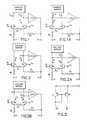
- A(s) is a frequency dependent term containing the poles and zeros which represent the frequency dependent gain of the internal gain stage illustrated.
- negative feedback seeks to maintain currents ie and im equal to each other, thus maintaining the base-emitter voltages of Qa and Qb equal, as was originally assumed.
- Ra and Rb do not influence the frequency dependent term of the expression for Vc, but since they do control the magnitude of the transfer functions Vc/Va, Vc/Vb, and Vc/Vr, closed loop gain and dynamic characteristics such as 3dB bandwidth are independent of each other.
- the common mode rejection of the amplifier is very good.
- Vbeqb represents the base-emitter voltage (Vbe) of transistor Qb. If current sources Isa and Isb are added to sink current from the emitter nodes of Qa and Qb, respectively, these transistors can be forward biased with positive collector current even when (Vb - Vbeqb) ⁇ Vr. Isa and Isb can be fixed or variable (signal) current sources.
- Vc [Va(1 + 2Rc/Ra) - Vb(Rc/Rb + 2Rc/Ra) + Vr(Rc/Rb) + (Isa - Isb)Rc]/(1 + Rc/A(s)).
- A(s) is employed in the inverting configuration. It does not matter, however, whether A(s) is any combination of current or voltage input, with current or voltage output.
- the DC accuracy of the circuit of Figure 1 is excellent. Because currents ie and ia are maintained nearly equal by the action of negative feedback, the base-emitter voltages of Qa and Qb will be kept nearly equal as long as the transistor characteristics are well matched. Likewise, bias currents at the inputs will be nearly equal. Because of finite Early Voltages in these transistors, however, some errors in input offset voltage and input bias currents may be caused. To prevent this, several steps may be taken.
- the current mirror may be modified to maintain the collector-base voltages of Qa and Qb equal; transistors Qa and Qb may be replaced with cascade transistor pairs; or darlington input pairs or other more complex input schemes may be used.
- the circuits illustrated in Figures 2, 2A, 2B and 6 also overcome this difficulty without lowering performance in other areas.
- the circuit of Figure 1A differs from that of Figure 1 described above only in that a non-inverting internal gain stage A(s) has been substituted for the inverting internal gain stage of Figure 1, and its input is the collector of transistor Qb, which is 180 degrees out of phase with the collector of transistor Qa. To accommodate this change the input and output of the current mirror have been exchanged, as illustrated in Figure 1A. These two sign changes cancel each other, so the input/output transfer function is the same as that described in detail above for Figure 1.
- the voltage mirror is placed in a shunt position with respect to the signal path of the overall amplifer, which prevents an increase in group delay of the signal, but allows an increase in the open loop gain of the overall amplifier. This facilitates stable closed loop operation over wider bandwidths. In the absence of the voltage mirror, open loop gain can be increased only by adding amplification in series with the signal path, thus increasing group delay as well.
- Av(s) is a voltage input amplifier, but it may have either a voltage output or a current output.
- the circuit of Figure 2 functions like that of Figure 1.
- circuit of Figure 2A differs from that of Figure 2 described above only in that a non-inverting internal gain stage Av(s) has been substituted for the inverting internal gain stage of Figure 2, and its input is the collector of transistor Qb, which is 180 degrees out of phase with the collector of transistor Qa. These two sign changes cancel each other, so the input/output transfer function is the same as that described in detail above for Figure 2.
- the circuit of Figure 2B differs from that of Figure 2 described above only in that a differential internal gain stage has been substituted for the inverting internal gain stage of Figure 2 or the non-inverting internal gain stage of Figure 2A. This increases the open loop gain by a factor of 2, but if this factor is thought of as being included in the gain of the inverting gain stage of Figure 2, the input/output transfer function remains the same as that for Figure 2.
- circuit of Figure 7 may be derived from the above analysis of the circuits illustrated in Figures 1, 1A, 2, 2A, 2B and 6.
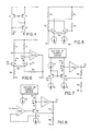
- Voltage Vb is fed directly to Ra without buffering from transistor Qb as before.
- transistor Qe is used to offset the base-emitter voltage of transistor Qa so that the non-inverting input at Va and inverting input at Ve are at nearly equal voltages.
- transistor Qa provides a low input impedance to enable current feedback.
- a current mirror, voltage mirror or resistive load at the collector of transistor Qa insures a stable operating point for the amplifier.
- Figure 8 illustrates another embodiment of the wideband feedback amplifier circuit of Figure 7, utilizing the same principles of operation.
- the input offset mechanism of the circuit of Figure 7 does not utilize feedback to control the offset voltage (Va - Ve) and does not buffer transistor Qa
- the circuit of Figure 8 provides both of these functions through the addition of a differential input amplifier D(s). Through negative feedback, the voltage Ve is forced to equal Va.
- the expression for Vc in the circuits of both Figure 7 and 8 is the same.
- a current mirror, voltage mirror or resistive load as before at the collector of transistor Qa insures a stable operating point for the amplifier.
- the circuits of Figures 7 and 8 eliminate the need for the bias control circuit taught in US-A-4 502 020.
- the present amplifier allows the DC bias to be stabilized by the use of a fixed current source reference rather than by using feedback as taught in the prior art. This greatly reduces circuit complexity and manufacturing costs.
Landscapes
- Engineering & Computer Science (AREA)
- Power Engineering (AREA)
- Amplifiers (AREA)
Applications Claiming Priority (2)
| Application Number | Priority Date | Filing Date | Title |
|---|---|---|---|
| US813590 | 1985-12-26 | ||
| US06/813,590 US4628279A (en) | 1985-12-26 | 1985-12-26 | Wideband feedback amplifier |
Publications (2)
| Publication Number | Publication Date |
|---|---|
| EP0227323A2 true EP0227323A2 (de) | 1987-07-01 |
| EP0227323A3 EP0227323A3 (de) | 1988-06-29 |
Family
ID=25212841
Family Applications (1)
| Application Number | Title | Priority Date | Filing Date |
|---|---|---|---|
| EP86309263A Withdrawn EP0227323A3 (de) | 1985-12-26 | 1986-11-27 | Gegengekoppelter Breitbandverstärker |
Country Status (3)
| Country | Link |
|---|---|
| US (1) | US4628279A (de) |
| EP (1) | EP0227323A3 (de) |
| JP (1) | JPS62222704A (de) |
Cited By (1)
| Publication number | Priority date | Publication date | Assignee | Title |
|---|---|---|---|---|
| EP0445879A1 (de) * | 1990-03-07 | 1991-09-11 | Koninklijke Philips Electronics N.V. | Breitband-Signalverstärker |
Families Citing this family (22)
| Publication number | Priority date | Publication date | Assignee | Title |
|---|---|---|---|---|
| US4780689A (en) * | 1987-07-20 | 1988-10-25 | Comlinear Corporation | Amplifier input circuit |
| US5003269A (en) * | 1989-05-12 | 1991-03-26 | Burr-Brown Corporation | Unity gain amplifier with high slew rate and high bandwidth |
| US5081410A (en) * | 1990-05-29 | 1992-01-14 | Harris Corporation | Band-gap reference |
| FR2665034A1 (fr) * | 1990-07-17 | 1992-01-24 | Philips Composants | Amplificateur large bande presentant des sorties separees. |
| US5177451A (en) * | 1991-07-26 | 1993-01-05 | Burr-Brown Corporation | Unity gain amplifier with high slew rate and high bandwidth |
| US5166637A (en) * | 1992-03-16 | 1992-11-24 | Analog Devices, Inc. | Distortion cancellation amplifier system |
| US5546048A (en) * | 1992-09-04 | 1996-08-13 | Hitachi, Ltd. | Amplifier and display apparatus employing the same |
| BE1007613A3 (nl) * | 1993-10-11 | 1995-08-22 | Philips Electronics Nv | Frekwentiecompensatiecircuit voor stabilisatie van een verschilversterker met kruisgekoppelde transistors. |
| US5627494A (en) * | 1995-12-04 | 1997-05-06 | Motorola, Inc. | High side current sense amplifier |
| US6002299A (en) * | 1997-06-10 | 1999-12-14 | Cirrus Logic, Inc. | High-order multipath operational amplifier with dynamic offset reduction, controlled saturation current limiting, and current feedback for enhanced conditional stability |
| US6369740B1 (en) | 1999-10-22 | 2002-04-09 | Eric J. Swanson | Programmable gain preamplifier coupled to an analog to digital converter |
| US6590517B1 (en) | 1999-10-22 | 2003-07-08 | Eric J. Swanson | Analog to digital conversion circuitry including backup conversion circuitry |
| US6414619B1 (en) | 1999-10-22 | 2002-07-02 | Eric J. Swanson | Autoranging analog to digital conversion circuitry |
| US6310518B1 (en) | 1999-10-22 | 2001-10-30 | Eric J. Swanson | Programmable gain preamplifier |
| US6466091B1 (en) | 2000-10-02 | 2002-10-15 | Cirrus Logic, Inc. | High order multi-path operational amplifier with reduced input referred offset |
| US6307430B1 (en) | 2000-10-02 | 2001-10-23 | Cirrus Logic, Inc. | Noise reduction technique in chopper stabilized amplifier |
| US6359512B1 (en) | 2001-01-18 | 2002-03-19 | Texas Instruments Incorporated | Slew rate boost circuitry and method |
| US6515540B1 (en) | 2001-12-10 | 2003-02-04 | Cirrus Logic, Inc. | High order multi-path operational amplifier with output saturation recovery |
| US9136807B2 (en) * | 2013-07-16 | 2015-09-15 | Analog Devices, Inc. | Apparatus and methods for electronic amplification |
| JP2015070774A (ja) * | 2013-10-01 | 2015-04-13 | 新日本無線株式会社 | スイッチング電源装置 |
| CN109075754B (zh) * | 2016-05-03 | 2023-04-14 | 哈曼国际工业有限公司 | 单端仪表折叠式栅-阴放大器 |
| US11502654B2 (en) | 2020-10-01 | 2022-11-15 | Harman International Industries, Incorporated | Single-ended differential transimpedance amplifier |
Family Cites Families (3)
| Publication number | Priority date | Publication date | Assignee | Title |
|---|---|---|---|---|
| US3733559A (en) * | 1970-06-29 | 1973-05-15 | Rca Corp | Differential amplifier |
| US4042886A (en) * | 1975-08-18 | 1977-08-16 | Motorola, Inc. | High input impedance amplifier circuit having temperature stable quiescent operating levels |
| US4358739A (en) * | 1980-02-11 | 1982-11-09 | Nelson David A | Wide-band direct-current coupled transistor amplifier |
-
1985
- 1985-12-26 US US06/813,590 patent/US4628279A/en not_active Expired - Lifetime
-
1986
- 1986-11-27 EP EP86309263A patent/EP0227323A3/de not_active Withdrawn
- 1986-12-25 JP JP61308076A patent/JPS62222704A/ja active Pending
Cited By (1)
| Publication number | Priority date | Publication date | Assignee | Title |
|---|---|---|---|---|
| EP0445879A1 (de) * | 1990-03-07 | 1991-09-11 | Koninklijke Philips Electronics N.V. | Breitband-Signalverstärker |
Also Published As
| Publication number | Publication date |
|---|---|
| EP0227323A3 (de) | 1988-06-29 |
| US4628279A (en) | 1986-12-09 |
| JPS62222704A (ja) | 1987-09-30 |
Similar Documents
| Publication | Publication Date | Title |
|---|---|---|
| US4628279A (en) | Wideband feedback amplifier | |
| EP0159757A2 (de) | Verstärker mit Eingangsfähigkeit über den gesamten Versorgungsspannungsbereich und geregelter Transkonduktanz | |
| US5351012A (en) | Low input resistance current-mode feedback operational amplifier input stage | |
| US6188280B1 (en) | Differential amplifier with gain linearization through transconductance compensation | |
| US4780689A (en) | Amplifier input circuit | |
| GB2179814A (en) | Operational amplifier | |
| EP0400819B1 (de) | Betriebsverstärker mit niedrigem Vorspannungsstrom und hoher Anstiegsgeschwindigkeit | |
| US4701719A (en) | Differential amplification circuit | |
| EP0730345B1 (de) | Schaltung mit variabler Verstärkung | |
| KR950005172B1 (ko) | 3-단자 연산증폭기 | |
| US5043675A (en) | Difference amplifier employing input attenuator network and powered by a single polarity power supply | |
| US4757273A (en) | Complementary transconductance amplifiers | |
| EP0164182B1 (de) | JFET Eingangsstufe mit aktiver Last | |
| EP0263572B1 (de) | Spannungsgesteuerte Push-pull-Stromquelle | |
| JP2733962B2 (ja) | 利得制御増幅器 | |
| US3908173A (en) | Differential amplifying system with forced differential feedback | |
| US4612513A (en) | Differential amplifier | |
| US4714894A (en) | Operational amplifier | |
| US4682059A (en) | Comparator input stage for interface with signal current | |
| US4521739A (en) | Low offset voltage transistor bridge transconductance amplifier | |
| US4167708A (en) | Transistor amplifier | |
| US6060870A (en) | Voltage-to-current converter with error correction | |
| EP0518673B1 (de) | Schnelle Pufferschaltung | |
| US6246290B1 (en) | High gain, current driven, high frequency amplifier | |
| EP0404403A2 (de) | Verstärker mit sehr niedriger Verzerrung |
Legal Events
| Date | Code | Title | Description |
|---|---|---|---|
| PUAI | Public reference made under article 153(3) epc to a published international application that has entered the european phase |
Free format text: ORIGINAL CODE: 0009012 |
|
| AK | Designated contracting states |
Kind code of ref document: A2 Designated state(s): DE FR GB |
|
| PUAL | Search report despatched |
Free format text: ORIGINAL CODE: 0009013 |
|
| AK | Designated contracting states |
Kind code of ref document: A3 Designated state(s): DE FR GB |
|
| STAA | Information on the status of an ep patent application or granted ep patent |
Free format text: STATUS: THE APPLICATION IS DEEMED TO BE WITHDRAWN |
|
| 18D | Application deemed to be withdrawn |
Effective date: 19881230 |
|
| RIN1 | Information on inventor provided before grant (corrected) |
Inventor name: NELSON, DAVID A. |