EP0228088A2 - Laser à surface émissive accordable - Google Patents
Laser à surface émissive accordable Download PDFInfo
- Publication number
- EP0228088A2 EP0228088A2 EP86118086A EP86118086A EP0228088A2 EP 0228088 A2 EP0228088 A2 EP 0228088A2 EP 86118086 A EP86118086 A EP 86118086A EP 86118086 A EP86118086 A EP 86118086A EP 0228088 A2 EP0228088 A2 EP 0228088A2
- Authority
- EP
- European Patent Office
- Prior art keywords
- waves
- grating
- wave
- waveguide
- apparatus defined
- Prior art date
- Legal status (The legal status is an assumption and is not a legal conclusion. Google has not performed a legal analysis and makes no representation as to the accuracy of the status listed.)
- Withdrawn
Links
Images


Classifications
-
- H—ELECTRICITY
- H01—ELECTRIC ELEMENTS
- H01S—DEVICES USING THE PROCESS OF LIGHT AMPLIFICATION BY STIMULATED EMISSION OF RADIATION [LASER] TO AMPLIFY OR GENERATE LIGHT; DEVICES USING STIMULATED EMISSION OF ELECTROMAGNETIC RADIATION IN WAVE RANGES OTHER THAN OPTICAL
- H01S5/00—Semiconductor lasers
- H01S5/10—Construction or shape of the optical resonator, e.g. extended or external cavity, coupled cavities, bent-guide, varying width, thickness or composition of the active region
- H01S5/18—Surface-emitting [SE] lasers, e.g. having both horizontal and vertical cavities
- H01S5/183—Surface-emitting [SE] lasers, e.g. having both horizontal and vertical cavities having only vertical cavities, e.g. vertical cavity surface-emitting lasers [VCSEL]
- H01S5/18308—Surface-emitting [SE] lasers, e.g. having both horizontal and vertical cavities having only vertical cavities, e.g. vertical cavity surface-emitting lasers [VCSEL] having a special structure for lateral current or light confinement
- H01S5/18319—Surface-emitting [SE] lasers, e.g. having both horizontal and vertical cavities having only vertical cavities, e.g. vertical cavity surface-emitting lasers [VCSEL] having a special structure for lateral current or light confinement comprising a periodical structure in lateral directions
-
- G—PHYSICS
- G02—OPTICS
- G02B—OPTICAL ELEMENTS, SYSTEMS OR APPARATUS
- G02B6/00—Light guides; Structural details of arrangements comprising light guides and other optical elements, e.g. couplings
- G02B6/10—Light guides; Structural details of arrangements comprising light guides and other optical elements, e.g. couplings of the optical waveguide type
- G02B6/12—Light guides; Structural details of arrangements comprising light guides and other optical elements, e.g. couplings of the optical waveguide type of the integrated circuit kind
- G02B6/122—Basic optical elements, e.g. light-guiding paths
- G02B6/124—Geodesic lenses or integrated gratings
-
- G—PHYSICS
- G02—OPTICS
- G02B—OPTICAL ELEMENTS, SYSTEMS OR APPARATUS
- G02B6/00—Light guides; Structural details of arrangements comprising light guides and other optical elements, e.g. couplings
- G02B6/24—Coupling light guides
- G02B6/42—Coupling light guides with opto-electronic elements
- G02B6/4201—Packages, e.g. shape, construction, internal or external details
- G02B6/4202—Packages, e.g. shape, construction, internal or external details for coupling an active element with fibres without intermediate optical elements, e.g. fibres with plane ends, fibres with shaped ends, bundles
-
- H—ELECTRICITY
- H01—ELECTRIC ELEMENTS
- H01S—DEVICES USING THE PROCESS OF LIGHT AMPLIFICATION BY STIMULATED EMISSION OF RADIATION [LASER] TO AMPLIFY OR GENERATE LIGHT; DEVICES USING STIMULATED EMISSION OF ELECTROMAGNETIC RADIATION IN WAVE RANGES OTHER THAN OPTICAL
- H01S5/00—Semiconductor lasers
- H01S5/10—Construction or shape of the optical resonator, e.g. extended or external cavity, coupled cavities, bent-guide, varying width, thickness or composition of the active region
- H01S5/12—Construction or shape of the optical resonator, e.g. extended or external cavity, coupled cavities, bent-guide, varying width, thickness or composition of the active region the resonator having a periodic structure, e.g. in distributed feedback [DFB] lasers
- H01S5/125—Distributed Bragg reflector [DBR] lasers
-
- H—ELECTRICITY
- H01—ELECTRIC ELEMENTS
- H01S—DEVICES USING THE PROCESS OF LIGHT AMPLIFICATION BY STIMULATED EMISSION OF RADIATION [LASER] TO AMPLIFY OR GENERATE LIGHT; DEVICES USING STIMULATED EMISSION OF ELECTROMAGNETIC RADIATION IN WAVE RANGES OTHER THAN OPTICAL
- H01S5/00—Semiconductor lasers
- H01S5/10—Construction or shape of the optical resonator, e.g. extended or external cavity, coupled cavities, bent-guide, varying width, thickness or composition of the active region
- H01S5/18—Surface-emitting [SE] lasers, e.g. having both horizontal and vertical cavities
- H01S5/185—Surface-emitting [SE] lasers, e.g. having both horizontal and vertical cavities having only horizontal cavities, e.g. horizontal cavity surface-emitting lasers [HCSEL]
- H01S5/187—Surface-emitting [SE] lasers, e.g. having both horizontal and vertical cavities having only horizontal cavities, e.g. horizontal cavity surface-emitting lasers [HCSEL] using Bragg reflection
-
- H—ELECTRICITY
- H10—SEMICONDUCTOR DEVICES; ELECTRIC SOLID-STATE DEVICES NOT OTHERWISE PROVIDED FOR
- H10F—INORGANIC SEMICONDUCTOR DEVICES SENSITIVE TO INFRARED RADIATION, LIGHT, ELECTROMAGNETIC RADIATION OF SHORTER WAVELENGTH OR CORPUSCULAR RADIATION
- H10F30/00—Individual radiation-sensitive semiconductor devices in which radiation controls the flow of current through the devices, e.g. photodetectors
- H10F30/20—Individual radiation-sensitive semiconductor devices in which radiation controls the flow of current through the devices, e.g. photodetectors the devices having potential barriers, e.g. phototransistors
- H10F30/21—Individual radiation-sensitive semiconductor devices in which radiation controls the flow of current through the devices, e.g. photodetectors the devices having potential barriers, e.g. phototransistors the devices being sensitive to infrared, visible or ultraviolet radiation
- H10F30/22—Individual radiation-sensitive semiconductor devices in which radiation controls the flow of current through the devices, e.g. photodetectors the devices having potential barriers, e.g. phototransistors the devices being sensitive to infrared, visible or ultraviolet radiation the devices having only one potential barrier, e.g. photodiodes
- H10F30/227—Individual radiation-sensitive semiconductor devices in which radiation controls the flow of current through the devices, e.g. photodetectors the devices having potential barriers, e.g. phototransistors the devices being sensitive to infrared, visible or ultraviolet radiation the devices having only one potential barrier, e.g. photodiodes the potential barrier being a Schottky barrier
-
- H—ELECTRICITY
- H10—SEMICONDUCTOR DEVICES; ELECTRIC SOLID-STATE DEVICES NOT OTHERWISE PROVIDED FOR
- H10F—INORGANIC SEMICONDUCTOR DEVICES SENSITIVE TO INFRARED RADIATION, LIGHT, ELECTROMAGNETIC RADIATION OF SHORTER WAVELENGTH OR CORPUSCULAR RADIATION
- H10F77/00—Constructional details of devices covered by this subclass
- H10F77/40—Optical elements or arrangements
- H10F77/413—Optical elements or arrangements directly associated or integrated with the devices, e.g. back reflectors
-
- H—ELECTRICITY
- H01—ELECTRIC ELEMENTS
- H01S—DEVICES USING THE PROCESS OF LIGHT AMPLIFICATION BY STIMULATED EMISSION OF RADIATION [LASER] TO AMPLIFY OR GENERATE LIGHT; DEVICES USING STIMULATED EMISSION OF ELECTROMAGNETIC RADIATION IN WAVE RANGES OTHER THAN OPTICAL
- H01S5/00—Semiconductor lasers
- H01S5/06—Arrangements for controlling the laser output parameters, e.g. by operating on the active medium
- H01S5/0604—Arrangements for controlling the laser output parameters, e.g. by operating on the active medium comprising a non-linear region, e.g. generating harmonics of the laser frequency
-
- H—ELECTRICITY
- H01—ELECTRIC ELEMENTS
- H01S—DEVICES USING THE PROCESS OF LIGHT AMPLIFICATION BY STIMULATED EMISSION OF RADIATION [LASER] TO AMPLIFY OR GENERATE LIGHT; DEVICES USING STIMULATED EMISSION OF ELECTROMAGNETIC RADIATION IN WAVE RANGES OTHER THAN OPTICAL
- H01S5/00—Semiconductor lasers
- H01S5/06—Arrangements for controlling the laser output parameters, e.g. by operating on the active medium
- H01S5/065—Mode locking; Mode suppression; Mode selection ; Self pulsating
- H01S5/0651—Mode control
- H01S5/0653—Mode suppression, e.g. specific multimode
- H01S5/0655—Single transverse or lateral mode emission
-
- H—ELECTRICITY
- H01—ELECTRIC ELEMENTS
- H01S—DEVICES USING THE PROCESS OF LIGHT AMPLIFICATION BY STIMULATED EMISSION OF RADIATION [LASER] TO AMPLIFY OR GENERATE LIGHT; DEVICES USING STIMULATED EMISSION OF ELECTROMAGNETIC RADIATION IN WAVE RANGES OTHER THAN OPTICAL
- H01S5/00—Semiconductor lasers
- H01S5/10—Construction or shape of the optical resonator, e.g. extended or external cavity, coupled cavities, bent-guide, varying width, thickness or composition of the active region
- H01S5/12—Construction or shape of the optical resonator, e.g. extended or external cavity, coupled cavities, bent-guide, varying width, thickness or composition of the active region the resonator having a periodic structure, e.g. in distributed feedback [DFB] lasers
- H01S5/1206—Construction or shape of the optical resonator, e.g. extended or external cavity, coupled cavities, bent-guide, varying width, thickness or composition of the active region the resonator having a periodic structure, e.g. in distributed feedback [DFB] lasers having a non constant or multiplicity of periods
- H01S5/1215—Multiplicity of periods
-
- H—ELECTRICITY
- H01—ELECTRIC ELEMENTS
- H01S—DEVICES USING THE PROCESS OF LIGHT AMPLIFICATION BY STIMULATED EMISSION OF RADIATION [LASER] TO AMPLIFY OR GENERATE LIGHT; DEVICES USING STIMULATED EMISSION OF ELECTROMAGNETIC RADIATION IN WAVE RANGES OTHER THAN OPTICAL
- H01S5/00—Semiconductor lasers
- H01S5/10—Construction or shape of the optical resonator, e.g. extended or external cavity, coupled cavities, bent-guide, varying width, thickness or composition of the active region
- H01S5/18—Surface-emitting [SE] lasers, e.g. having both horizontal and vertical cavities
- H01S5/183—Surface-emitting [SE] lasers, e.g. having both horizontal and vertical cavities having only vertical cavities, e.g. vertical cavity surface-emitting lasers [VCSEL]
- H01S5/18386—Details of the emission surface for influencing the near- or far-field, e.g. a grating on the surface
- H01S5/18394—Apertures, e.g. defined by the shape of the upper electrode
Definitions
- the present invention relates to apparatus (devices) for controlling and guiding waves such as waves of electromagnetic radiation, acoustic waves, pressure waves, electron waves and the like.
- This apparatus includes at least one transmitting medium for guiding the wave energy.
- the apparatus may take the form of a "sandwich”-type or thin film waveguide, in which case the transmitting medium has at least one curvi-planar boundary.
- the apparatus may take the form of a "rod"-shaped or cylindrical waveguide, in which case the transmitting medium has a substantially cylindrical boundary.
- the apparatus may also take the form of a "sphere"-shaped structure, in which case the transmitting medium has a substantially closed surface.
- Wavelength and direction-selective diffraction of acoustic or electromagnetic waves is conveniently achieved by an arrangement called a “diffraction grating” or “Bragg reflector".
- a “diffraction grating” is comprised of a large number of substantially parallel and equidistant “grating lines” which produce controlled scattering of waves.
- the “grating lines” may be created by variations in relief of a wave-reflecting surface, or by variations in some aspects of a wave-transmitting medium which varies some aspects of the waves propagating within the medium.
- the lines may be formed by variations in the index of refraction - which determines the velocity of waves within the transmitting medium - or variations in the "gain constant " - i.e., the constant of wave amplification or attenuation - at successive lines or points within the medium.
- a one-dimensional grating consists of a plurality of parallel, equidistant and linear grating lines on a transparent or reflecting planar or concave surface.
- the grating lines may be alternatively more or less absorbing, giving an amplitude grating, or varying in relief or refractive index in an alternating manner, giving a phase grating.
- a two-dimensional grating may be formed, for example, by a pair of one-dimensional gratings superimposed at a certain angle or by circular or spiral grating lines provided on a planar surface. Three-dimensional diffraction gratings occur naturally, for example in crystals, due to the ordering of molecules along straight lines.
- Joseph Fraunhofer is generally regarded as the inventor of diffraction gratings. He scribed small grating lines on a planar, reflecting surface in 1823, developed their geometrical theory and used them to make surprisingly accurate wavelength calibrations of solar absorption lines.
- the U.S. Patent No. 3,970,959 to Wang et al. teaches the application of a two-dimensional diffraction grating to thin film optical wave guides. These gratings serve to reflect or scatter light waves into controllable transverse modes of propagation.
- the U.S. Patent No. 4,006,432 to Streifer et al. utilizes a one-dimensional grating in a heterojunction diode laser to produce a highly collimated, polarized light beam perpendicular to the plane of the PN junction (which is the plane of the thin film waveguide structure).
- Patent No.4,140,362 to Tien discloses techniques for producing two-dimensional curved line diffraction gratings on a thin film optical device.
- the purpose of such gratings is to focus as well as diffract light that is confined to the film - i.e., the "optical waveguide" - in which the grating is formed.
- these grating lines produced by Tien form only a segment of a circle, completely circular and spiral diffraction gratings are also known from the article by Dyson (Ref. 4, above).
- Resonators for optical wave lasers have been built by replacing the end mirrors by diffraction gratings, eventually combining them into one grating extending over the entire length of the light-amplifying medium (Ref. 5, above). Furthermore, a planar film waveguide containing a one-dimensional grating has been considered as an optical resonator with laser emission at an angle-to the plane of the film waveguide (Ref. 7, above).
- the change of the refractive index due to an electric field is used for frequency modulation.
- the wavelength shift of the maximum of the optical amplification over several lonitudinal modes is used for tuning of the laser wavelength.
- nonlinear optics to optical waveguides is of great current interest, since the waveguide confines the optical-intensity to a small area given by the cross-section of the waveguide and maintains a high optical intensity over a longer propagation distance. It is not known, however, to further concentrate the optical intensity within a waveguide by a diffraction grating. More particularly, it is not known to concentrate in a thin film waveguide optical intensity in the center of a standing wave pattern produced by a cylindrical diffraction grating.
- a diffraction grating having a plurality of substantially closed loop grating lines consecutively enclosing each other from inner to outer, with all of the grating lines extending substantially parallel to the phase fronts of the guided waves.
- the "sandwich" type structure for controlling waves according to the invention includes a waveguide configured to confine and guide propagating waves and comprising at least one wave-transmitting medium having a - curvi-planar boundary and a diffraction grating for scattering wave energy into or out of the guided waves.
- the diffraction grating includes a large number of substantially closed loop grating lines consecutively enclosing each other from inner to outer. All of these grating lines extend substantially parallel to the wave phase fronts of the guided wave.
- the "rod"-shaped structure for controlling waves comprises a wave-transmitting medium having a substantially cylindrical boundary and means, such as mirrors or a diffraction grating, for reflecting waves back and forth in the axial direction within this medium.
- a separate diffraction grating is disposed on the cylindrical boundary for diffracting power into or out of the counter-propagating waves forming the standing waves.
- This grating comprises a large number of substantially closed loop grooves, which extend along the cylindrical boundary in planes parallel to the phase fronts of the guided waves.
- cylindrical is employed in its general mathematical sense to denote a shape having the form or properties of a "cylinder”.
- Webster's Colle g iate Dictionary defines a cylinder as "the surface traced by a straight line moving parallel to a fixed straight line and intersecting a fixed curve". This fixed curve is normally a closed loop of arbitrary shape, so that the cylinder is formed by a closed loop surface which is parallel at every point to a fixed straight line.
- the "sphere"-shaped structure for controlling-a first group of waves comprises a wave- transmitting medium and a diffraction grating associated with this medium for storing the energy of this first group of waves.
- This diffraction grating comprises a large number of substantially closed surface grating shells, which enclose each other from inner to outer and which extend substantially parallel to the phase fronts of this first group of waves.
- the energy stored in this first group of waves is transferred to a second group of waves by absorption of wave energy in the grating shells.
- the resonator may take the form of a "rod"-shaped structure as explained above, but having arranged within the resonator externally controllable means for extracting energy from the oscillator wave. By moderately modulating the energy extraction efficiency of this means so that the intensity of the oscillator wave is essentially unperturbed, the frequency of the oscillator wave is modulated efficiently.
- the resonator may also comprise several "rod"-shaped waveguide structures, which are coupled via a thin film waveguide. By modulating the spatial distribution of the energy extraction within the resonator, the mode content of the oscillator wave is modulated.
- Figs. 1A and 1B and Figs. 2A and 2B illustrate waveguides of curvi-planar and curvi-linear cylindrical shape, respectively, which are provided with diffraction gratings in accordance with the principles of the present invention.
- the x, y and z Cartesian coordinates and the r and ⁇ polar coordinates are indicated to provide orientation.
- the waveguide of Figs. 1A and 1B has a "sandwich” structure which is slightly curved (i.e., spherical) in the x-y direction.
- the waveguide of Figs. 2A and 2B has a "rod” shape which exhibits a slight curve along its central (z) axis.
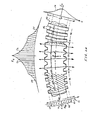
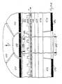
- Fig. 1 Considering first the waveguide of Figs. 1A and 1B (hereinafter referred to as "Fig. 1") there is shown a cross-section of the sandwich structure comprising a central wave . transmitting layer 10, two wave transmitting "cladding” layers 12 and 14, an anti-reflection layer 16 and a reflective or mirror layer 18.
- the index of refraction n of the central layer is I higher than the indices of refraction n , n of the cladding 2 3 layers 12 and 14, respectively.
- the central and cladding layers thus serve as a waveguide for electromagnetic radiation (EMR) in the infrared, visible light or ultraviolet light spectra. The transmission of such radiation along the waveguide is indicated by the arrows 19.
- EMR electromagnetic radiation
- the boundary between the central layer 10 and the cladding layer 12 includes a plurality of substantially closed loop ridges and grooves which form a diffraction grating.
- the dimensions of these ridges and grooves will be discussed later. Suffice it to say at this point that they are in the order of the wavelength of the electromagnetic radiation transmitted in the waveguide.
- Fig. 1B shows the diffraction grating in plan view, with the bottoms of the grooves (i.e., the surfaces of the cladding layer 12 facing the central layer 10 which are closest to the cladding layer 14) indicated in solid.black.
- the grooves are substantially circular and coaxial; i.e., they successively enclose each other from the innermost groove outward.
- the diffraction grating is divided into two parts: a center part 20 and a surrounding, outer part 22.
- the widths of both the ridges and grooves in the center part are larger than those of the outer part.
- the grooves in the center part are trapezoidal-shaped in cross section, whereas the grooves in the outer part have a rectangular cross section.
- the grating lines of the outer part 22 are interrupted in a sector shaped region 23, which means that the region 23 is uncorrugated.
- the region 23 is bounded by two lines 24 and 25, which run perpendicular to the ridges and grooves.
- Fig. 1A are graphs of the index of refraction, n(z) of the waveguide layers; the intensity distribution I , along the x axis within the central layer 10 of the waveguide; and the axial intensity distribution I , at the center of the grating.
- the refractive index n varies along the z axis as indicated by the characteristic 26.
- the characteristic 26 reaches a maximum equal to the refractive index n along the 1 portion of the z axis containing the central layer 10, and falls off in the cladding layers 12 and 14 which have indices of refraction n and n , respectively.
- the index n depends upon the respective widths of the ridges and grooves of the grating.
- the shaded rectangle 28 has a length along the z axis equal to the effective width T of the axial intensity distribution I and a eff z height along the n axis equal to the effective refractive index n of the waveguide.
- T and n will be eff eff eff defined further below.
- the graph in the upper portion of Fig. lA shows that the intensity distribution falls off toward the outside of the grating as indicated by the characteristics 29 and 30.
- the center part 20 of the diffraction grating couples EMR out of the waveguide. This causes the exponential decrease according to the curves 29.
- the EMR is back reflected toward the center of the grating. This causes an even more abrupt exponential decrease of the intensity as indicated by the curves 30.
- Fig. lA Shown within the sandwich structure of Fig. lA are bidirectional rays 34, directed perpendicular to the plane of the waveguide, and rays 36 which are reflected back by the grating in the plane of the waveguide.
- the rays 34 which are emitted in the negative direction of the z axis are reflected by the mirror layer 18 in the opposite direction.
- These rays, together with the rays that are emitted in the positive direction of the z axis pass out of the waveguide through the anti-reflection layer 16 into free space. Because of the spherical curvature of the waveguide structure, the bundle of rays 34 is focused at a point (not shown) along the z axis. If the sandwich structure of Fig. lA were completely planar in the x and y directions, the rays 34 would be substantially parallel.
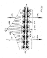
- a rod-shaped waveguide made of wave transmitting core material 40 having an index of refraction n . 4
- the core 40 is surrounded by air or vacuum, which acts as a cladding layer.
- Etched into the outer circumference are a plurality of ridges and grooves 42 forming a diffraction grating.
- These ridges (grooves) are coaxial and extend in planes perpendicular to the rod axis (z axis).
- the grooves are arranged in three parts: a center part 44 and outer parts 46.
- the grooves (ridges) are equally spaced, and within the outer parts 46 the grooves (ridges) are equally spaced.
- the spacing of the grooves in the center part is designed to couple EMR energy out of the waveguide, whereas the spacing of the grooves in the outer part is designed to couple wave energy travelling in the z axis direction backward.
- Fig. 2A shows at opposite ends of the rod-like structure and along its upper side, graphs of (1) the refractive index, (2) the distribution of intensity within the waveguide in the z direction, and (3) the distribution of intensity within the waveguide along the radius r (or, in this case, the x axis).
- the refractive index is equal to n 4 across the cross section of the rod and falls abruptly to the vacuum index outside as indicated by the curve 48. Only in the areas 50 of the grating, where the waveguide material is interrupted by air or vacuum, n depends upon the respective widths of the ridges and grooves of the grating.
- the shaded rectangle 51 illustrates again the quantities T and n as eff eff defined further below.
- the curves 52 of the intensity in the region of the center part 44 of the diffraction grating and the curves 54 in the regions of the outer parts 46 of the grating are exponentials, and are essentially identical to the corresponding curves 29 and 30 for the sandwich structure of Fig. 1.
- the curve 56 shows the intensity distribution along the x axis for the fundamental mode of the rod-like waveguide and has indicated the width T of the intensity eff distribution.
- the intensity distribution extends into the air, which acts as a cladding layer.
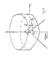
- Fig. 3 illustrates this coordinate system in which the z axis coincides with the cylinder axis, r is the distance of a point from the cylinder axis and ⁇ is the angular position of the point. Also shown is the field vector H of the axial directed z magnetic field and the field vector E of the circumferentially directed electric field.
- the axial directed electric field E and the axial directed magnetic z field H can be considered as the generating field components of z the total electromagnetic field, which means that all other field components can be derived from E and H .
- Maxwell's equations z z for these axial field components can be separated into two sets of scalar wave equations: where K and K , the axial and radial propagation constants, z r respectively, are related via the equation: These constants K and K will be further specified below.
- n is the refractive index of the waveguide layer at the point where the field is evaluated.
- the equation (1) describes the z dependence of the axial field components and the equation (2) describes the r, 0 dependence of the axial field components.
- the guided wave in the waveguide structure of Fig. 1 is considered to be monochromatic with the free space wavelength ⁇ and to be confined to a single waveguide mode, which has only the axial magnetic field H as z generating field component (E ⁇ 0).
- the solution of equation (1) z for each waveguide layer yields the z-dependence of the axial magnetic field H and therefrom derived the z-dependence of the z circumferential electric field E ⁇ ⁇ H z / ⁇ r. 2
- n is the effective refractive index of eff the waveguide, which can be interpreted as a field-weighted average of the indices of refraction of the different waveguide layers.
- the quantities n and T characterize an effective eff eff dielectric waveguide, which will be used for the description of the action of the grating-waveguide configuration.
- the concept of the effective dielectric waveguide encounters a wide class of waveguides.
- the model is particularly useful for the description of a waveguide with a graded refractive index as shown in Fig. 1 or of a multilayer waveguide such as a multiple quantum well waveguide. It is noted that the model also applies to a waveguide with one or several metal boundaries such as a metal hollow waveguide.
- the Bessel function J and its derivative J ' 1 1 are illustrated in Fig. 4A as a function of the radius r, for a range of small radii and for a range of larger radii, respectively.
- the vertical scale in the left- hand portion of the diagram is smaller than the vertical scale in the right-hand portion.
- the magnitude of the functions J and J 1 ' are greater near the left-hand (z) axis than toward the right.
- the standing wave pattern corresponding to a pair of coefficients h and e is m m characterized, in particular, by its number of radial directed nodal lines, along which the cosine function, and therefore H z and E ⁇ vanish.
- the standing wave pattern corresponding to a pair of coefficients h and e is usually denoted as the mode of the m m circumferential order m.
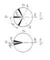
- the Figs. 5A, 5B and 5C illustrate phase fronts of field E ⁇ by the line 124, 126 and 128, respectively.
- E is the electric field component of a standing wave
- the shaded areas illustrate pockets of stored wave energy.
- the arrows 136, 138 and 140 within the energy pockets illustrate the direction of the electric field.
- the circumferentially oriented field is symmetric (antisymmetric) with respect to the field center for modes with odd (even) integer order m, as illustrated by the arrows 136, 138 and 140.
- Radial directed nodal lines 142 and 143 are also shown.
- a field free area 144 and 145 in the center of the standing wave pattern can be seen.
- a waveguide according to Fig. 1 provided with a nonlinear material (for example LiNbO , ZnS or a nonlinear 3 organic material), for example in the cladding layer 12 or the central layer 10, the cylindrical grating in the waveguide is a promising arrangement to enhance nonlinear interactions.
- This attractive feature of the arrangement in Fig. 1 can be used for frequency conversion (via second order nonlinearities) or for affecting the z dependence of the field distribution by intensity-induced refractive index changes (using third order nonlinearities).
- a waveguide according to Fig. 1 with an electro- absorptive material for example GaAs, Al Ga As, InP, Ga In p 1-p p 1-p As P
- q 1-q the absorption of resonator modes can be influenced by applying an electric field perpendicular to the layers.
- Such an electric field can be built up by reverse biasing a pn junction formed by two of the mentioned semiconductor materials. The influence of this electric field will be particularly high, if it is applied in the area around the center of the grating.
- the influence of the electric field is different for waveguide modes which have E as the generating axial field component than for the waveguide modes which have H as the generating axial field component.
- the wavelength of m the guided wave in the mode of the circumferential order m is now defined as twice the radial distance between two neighboring circumferential nodal lines 150 and 151 of the electric field component E .
- the circumferential nodal lines 150 and 151 are illustrated in Fig. 5B.
- the functions J and J' follow essentially the trigonometric m m functions: which have the zeros equally spaced.
- the wavelength of the guided wave is therefore essentially given by which would be equal to the wavelength of a guided wave with plane wave fronts.
- Fig. 4A shows the wavelength ⁇ , in the range of small radii, where the wavelength ⁇ , slightly varies with r and in the 1 range of larger radii, where the wavelength A is essentially 1 constant.
- the action of the grating on a guided wave will now be described in greater detail.
- To efficiently extract power from a guided wave with circular cylindrical phase fronts by means of a grating it is useful to have the ridges and grooves of the grating arranged in concentric circles. The ridges extend then perpendicular to the direction of propagation of the wave or, equivalently, parallel to the phase fronts of the wave.
- the effect of the grating on the waveguide properties can be modelled by relating the changes of the position of the boundary containing the grating to changes of the effective thickness T and of the effective refractive eff index n of the waveguide.
- Fig. 4B shows schematically the eff radial variation of the effective thickness of the waveguide along the x axis due to the ridges of the waveguide structure in Fig. 1.
- the radial variation of the effective refractive index is illustrated by the more or less shaded areas within the center part 152 and the outer part 153 of the effective dielectric waveguide.
- each ridge in the central layer in Fig. lA therefore corresponds to an effective boundary displacement 160 on the opposite side in the effective dielectric waveguide and to a region of higher effective refractive index in Fig. 4B.
- Fig. 6 shows a magnified portion of the center part of the effective dielectric waveguide structure.
- the sides of each effective boundary displacement 160, 161 or 162 are two regions 164 and 165 with a change ⁇ T effective thickness and a eff change ⁇ n of the effective refractive index along the ray eff 154.
- Each effective boundary displacement has an average radial width W.
- Neighboring boundary displacements 160 and 161 are the radial distance apart.
- the electric field E out of the outgoing wave in the presence of a waveguide in homogenity in the region 164 is thought to cause a scattered wave with a magnetic field vector H and an rad electric field vector E .
- the scattered wave propagates in rad the direction of the ray 166.
- the range of angles 8, in which scattering occurs is relatively large, as illustrated by the phase front 168, due to the small extension of the waveguide in homogeneity in region 164 of the order or smaller than the wavelength ⁇ .
- the widening (narrowing) of the guide in the region 164 (165) causes a bending of the ray 154 toward greater (smaller) values of the z-coordinate and a diffraction of radiation in the direction of the ray 170 (172), which is preferentially oriented toward increasing r-values.
- the increasing (decreasing) effective refractive index in the region 164 (165) causes a reflection of radiation in the direction of the ray 174 (176), which is preferentially oriented toward decreasing r-values.
- the superposition of the rays 178 and 179 diffracted from two neighboring regions 180 and 181 corresponding to the region 164 yields a condition for the angles 8 of emission of the grating c due to multiple constructive interference.
- Mathematically expressed the rays 178 and 179 are in phase, if where ⁇ and are noted, j is an integer and B is the distance m shown in Fig. 6 along the ray 178 from the ray 154 at the center of the region 180 to the wayefront that passes through the center of the region 181.
- the emission out of the waveguide can be enhanced, if scattering of power from the outgoing to the incoming wave is cancelled by destructive interference.
- the two rays 174 and 176 would be out of phase, if where W and ⁇ are noted, k is an integer and ⁇ and ⁇ are m 1 2 the phase changes of the rays 174 and 176, respectively, after scattering in the regions 164 and 165 due to changes of the effective refractive index, respectively.
- the radial spacing ⁇ is chosen to be equal to ⁇
- the 1 radial width W is chosen to be equal to ⁇ 1 2 so that the coupling of power of an outgoing guided wave with the wavelength ⁇ 1 into a vertical directed beam is maximized.
- Equation (16) solved for W yields Equation (17) means that the back reflection of the outgoing wave can be made particularly efficient, if the radial width of the boundary displacements is equal to a quarter wavelength in the guide or an odd integer multiple thereof.
- the radial distance ⁇ is chosen equal to ⁇ /2 and 1 the radial width W is chosen equal to ⁇ /4, as to maximize the 1 reflection of an outgoing guided wave with the wavelength ⁇ into 1 an incoming guided wave.
- the position of the boundary displacements has to be "fine tuned" with respect to the phase fronts of the standing wave pattern of this mode.
- the waveguide inhomogeneities corresponding to the region 192, which produce an increase of the effective refractive index along the ray 154, have to be placed at the loci of the maximum absolute values of the magnetic field H z .
- each grating line extracts power from the outgoing ray 154 and couples it in phase to the incoming ray.
- the amount of wave energy stored in the rings of wave energy pockets 132 illustrated in Fig. 5 decreases then exponentially with increasing radius.
- the exponential decrease of the radial intensity is illustrated by the curves 30 in Fig. lA.
- the ray 200 of an incoming guided wave is bent toward increasing z-values in the region 202.
- vertical rays 178 and 204 are in phase, if where the width W of the boundary displacement 160 is noted, i is an integer and p and ⁇ are the phase of the outgoing ray 154 out in at the center of the region 180 and the phase of the incoming ray 200 at the center of the region 202, respectively.
- the rays 154 and 200 of the counter propagating waves are in phase at radii where the absolute value of the electric field E of the standing wave is at a maximum.
- equation (18) one considers the rays 154 and 200 at two radii, which differ by the width W.
- the emitted rays 178 and 204 are then in phase, if they begin at radii which are essentially symmetric with respect to a radius with maximum absolute value of the electric field E .
- the total effect of two vertical rays 178 and 204 can be equivalently described by one vertical ray 205 outgoing from the rays 154 or 200 in the middle, between the two regions 180 and 202, where the absolute value of the field E is at a maximum.
- each grating line extracts power from the standing wave.
- the intensity of the standing wave decreases then exponentially with increasing radius as illustrated by the curves 29 in Fig. 1A.
- Fig. 7 shows a magnified view of the effective dielectric waveguide in Fig. 6 so that the curvature of the waveguide becomes visible.
- the radially fine tuned boundary displacements 210 and 212 scatter power out of the standing wave into the rays 214 and 216, as explained in conjunction with Fig. 6.
- the rays 214 and 216 describe the total effect of the respective boundary displacements and can therefore be thought to begin in the middle of the boundary displacements.
- the electric field E is symmetric with respect to the z axis. Therefore, the vectors of the electric field E in the middle of the boundary displacements 210 and 212 are equally directed as shown in Fig. 7. It is clear from Fig. 7 that the rays 214 and 216 are in phase along the z axis. Since the waveguide is curved, like a part of the surface of a sphere, all rays which are emitted perpendicular to the waveguide plane are in phase at the center of the sphere 218. The vertical emitted radiation is therefore focussed at the center of the sphere 218.
- the emitted beam is symmetric with respect to the nodal line and is linearly polarized in the direction of the nodal line.
- the wave energy contained in a ring of energy pockets 132 decreases exponentially with increasing radius of the ring, due to the extraction of power out of the standing wave by the grating lines.
- the far field of the emitted radiation is therefore highly collimated around an emission angle of ⁇ /2 and has a low side lobe level.
- a standing wave pattern of a mode with an even number m of nodal lines would produce an antisymmetric far field pattern, because of the antisymmetric electric field distribution mentioned in conjunction with Fig. 5A. This means in particular that this mode would not produce emission perpendicular to the waveguide plane.
- the far field pattern would be given by a large number of cones highly collimated around the axis corresponding to vertical emission.
- the grating lines of the outer part 22 are interrupted within a sector-shaped region 23 as can be seen in Fig. 1B.
- the radially counter propagating waves forming a standing wave are not back reflected within this uncorrugated region. Therefore, the quality factors of the resonator modes are reduced by the region 23.
- the resonator modes, which have a radial nodal line in the center of the region 23 suffer less extraction of wave energy.
- a mode with.a particular circumferential order m can be selected by loading the resonator with losses in the area between the lines 24 and 25, which run perpendicular to the grating lines.
- the losses can be introduced, in particular, by varying the cross-section of the ridges and grooves circumferentially such that they provide less back reflection in the area between those lines, or by modifying the waveguide layers such that they absorb or scatter more power out of the guided wave in the area between those lines.
- the more modes of consecutive orders m will contribute to the standing wave pattern, the more homogeneous will be the radial distribution of the stored wave energy. As a consequence, the volume energy density stored in the center part 20 in an ensemble of modes will be more homogeneous.
- a homogeneous energy density is useful, for example, in extracting a high total power from the resonator.
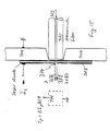
- Fig. 8 shows a . magnified portion of the center part 20 in Fig. 1.
- the ray 226 of the outgoing wave is bent toward the cladding layer 14 in the region 224 and scatters power into the ray 228.
- the ray 228 propagates toward increasing z values.
- the ray 228 scatters power along a ray 229 into the direction of the ray 230 of the incoming guided wave.
- the rays 229 and 230 can be in or out of phase, depending on the spacing S, so that power is added to or extracted from the guided wave.
- the ray 228 leaves the waveguide through the cladding layer 12.
- the ray 230 of the incoming wave is bent toward the cladding layer 12 in the region 224 and scatters power into the ray 232, which leaves the waveguide through the cladding layer 12.
- the spacing S of the mirror layer 18 to the center line of the waveguide which is given by the rays 226 or 230, is chosen such that the emitted rays 228 and 232 enhance each other as much as possible.
- the rays 228 and 232 are in phase, if where ⁇ , ⁇ , ⁇ and n , are noted, in out 1 is the average along the z axis of the graded refractive index n, S and S are the distances shown in Fig. 8, ⁇ is the 2 1 2 m phase change of the ray 228 due to the reflection at the mirror layer and k is an integer.
- ⁇ is chosen m equal to ⁇ radians, which is the phase change of optical radiation at a high reflectivity gold layer.
- the optimum optical path length S depends through ⁇ out - ⁇ in on the out in width W of the ridge 220 and on the fine tuning of the radial position of the ridges, as explained in conjunction with Fig. 6.
- Equation (21) In dielectric waveguides the refractive indices n and n 1 2 are often only slightly different so that one can set n ⁇ n ⁇ 1 2 n to a first approximation. Equation (21) then reduces to eff where the spacing S is noted and shown in Fig. 8. Equation (23) means that the spacing S has to be approximately equal to an integer multiple of one half of the wavelength X/n in the eff waveguide.
- the righthand portion of the Fig. 8 shows the intensity 2 distribution E of the standing wave due to the reflection of rad the ray 228.
- the electric field E of the emitted ray 228 is rad parallel to the layers as has been illustrated in Fig. 6.
- the 2 intensity distribution E has therefore a node at the (metal) rad mirror layer 18.
- the layer 14 thus stores wave energy in a standing wave pattern, thereby forming an external resonator coupled to the guided-wave resonator.
- the amount 2 of stored energy increases.
- the total quality factor of the two coupled resonators then also increases accordingly.
- Fig. 9 illustrates a grating with elliptical grating lines, which can replace the circular grating in both the center part 20 and the outer part 22 in Fig. 1.
- Fig. 9 the tops of the ridges in the central layer 10 are shown in solid black.
- Cartesian coordinates (x,y) and polar coordinates (r, ⁇ ) are provided for orientation.
- the eff eff ellipses can be expressed by: where c is noted and a is the longer half axis of the ellipse.
- the connection line of the two foci coincides with the x axis, and the center ⁇ of the coordinate system is midway between the two foci.
- a cylindrical wave with elliptical phase fronts can be described to a first approximation by the superposition of two in-phase circular cylindrical waves of equal amplitude, which have their axes at the foci F and F , respectively. This will 1 2 be explained below in greater detail. Since the distance 2c between the foci F and F in Fig. 9 is equal to a multiple of 1 2 the wavelength ⁇ /n , the circular cylindrical waves eff essentially interfere constructively along the x axis outside the connection line F F of the foci.
- the eff grating is operated along the x axis at one of its Bragg wavelengths according to equation (15) (second order grating).
- the width W of the ridges along the x axis substantially equal to ⁇ /(4n the back reflection of an eff outgoing wave into an incoming wave is made particularly efficient according to equation (17).
- the position of the ridges is then fine tuned for achieving a standing wave pattern along the x axis for both circular cylindrical waves, as has been outlined in conjunction with the regions 192 and 193 in Fig. 4B.
- the elliptical mode with one nodal line along the y axis has a particularly high quality factor due to back reflection of an outgoing wave by the grating. Since we have the spacing ⁇ of the ridges equal to the wavelength in the guide (second order grating), the grating is also coupling power from this resonator mode into a beam directed substantially.vertically out of the plane of the waveguide.
- the Mathieu functions which give an exact description of waves with elliptical phase fronts.
- the superposition of two field solutions also represents a solution.
- the grating lines which are provided in the waveguide, follow the curvature of the phase fronts of such a solution. Special grating curvatures can be of interest, for example to achieve a particular amplitude distribution or polarization of the beam emitted from the waveguide.
- Fig. 10 illustrates the superposition of these two primary waves.
- the primary waves are represented by the respective wave - vectors k and k and the vectors E and E of the respective electric fields.
- the wave vectors point in the directions of propagation of the primary waves.
- the electric field vectors E and E 0 ⁇ 2 are perpendicular to the respective wave vectors and are oriented tangential to the respective phase fronts 250 and 252.
- the vector E of the electric field of the sum wave is oriented tangential to the phase front 254 of the sum wave.
- the normal vector k to the field vector E represents the wave vector of the sum wave.
- the wave vector k is oriented tangential to the ray 256 of the sum wave.
- each point together with its respective tangent is called an element of the field of tangents.
- the field 260 of directions of propagation by drawing in each point the direction of the normal to the tangent.
- Each point together with its respective direction of propagation is called an element of the field of directions.
- Successively connecting elements of the field of directions yields a ray 256 of the sum wave.
- Correspondingly successively connecting elements of the field of tangents yields a phase front 254 of the sum wave due to the superposition of two in phase circular cylindrical primary waves.
- phase fronts may be constructed by superimposing an infinite number of circular cylindrical waves with different amplitudes and phases and with their axes parallel shifted to one another.
- a wave with cylindrical phase fronts thus is thought to be composed of a plurality of circular cylindrical waves (Huygen's principle).
- the curvatures of the phase fronts which prescribe the curvatures of the grating lines and the curvatures of the rays, along which wave propagation takes place, can be constructed by means of the field of tangents to phase fronts and the field of directions of propagation defined above.
- Fig. 11 shows the superposition of the two primary circular cylindrical waves in .greater detail. If one goes a small distance along the phase front 254 from the point P, to the point P the phase front 250 has to go forward (in the direction of k ,) by the length dr and 1 1 the phase front 252 has to go backward (opposite to the direction of k ) by the length dr . Mathematically, it is 2 2 where the angles ⁇ and ⁇ are shown in Fig. 11. The negative 1 2 sign occurs, since the phase fronts 252 is going backward. From the diagram of the electric field vectors in Fig.
- Equation 30 is the differential equation of a phase front in terms of the coordinates r and r .
- Equation (30) gives then approximately where d is a constant for each phase front.
- the constant d can be expressed for example by distances measured along the axis running through the two centers of the primary waves. In Fig. 10 this axis coincides with the x-axis.
- the phase front 254 intersects the x axis at the distance a from the point 0 in the middle between the two centers of the primary waves.
- r a + c
- r a - c
- Figs. 12A and 12B illustrate a distributed feedback (“DFB") semiconductor diode laser in which stimulated emission is enhanced by an arrangement similar to that shown in Fig. 1.
- DFB distributed feedback
- further means are provided according to the invention for efficient coupling of a waveguide mode and a vertical beam and for resonator mode selection.
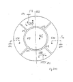
- Fig. 12A shows a cross-section of the laser device with a resonator similar to Fig. 1.
- the resonator is divided radially into a center part 300 and an outer part 302.
- the center part 300 contains a circular grating 304, which diffracts power out of waveguide mode mainly into substantially vertical beams 306 and 307, and contains a circular layer 308 capable of emission and amplification of optical radiation.
- the outer part 302 contains a grating 310, which provides mode selective distributed feedback, and contains an absorptive region 312 to select the resonator mode with one nodal line.
- the grating 304 of the center part and the grating 310 of the outer part are both in the lower cladding layer 324.
- Fig. 12B shows a schematic top view of the gratings of the center and the outer parts and has indicated Cartesian (x, y) coordinates.
- the cross-section of the arrangement in the Fig. 12A is oriented along the y axis.
- the resonator is built into a luminescence diode energized by carrier injection through a pair of contacts 314 and 316 in the form of rings, to allow vertical emitted radiation to leave the resonator.
- the contact 316 also acts as a mirror layer in the center part 300.
- the layer thicknesses of the waveguide in the center part 300 are fine tuned such that the beam 307 emitted from the grating 304 and reflected from the mirror 316 maximally enhances the power in the beam 306 emitted from the grating 304 in the other direction. This adjustment of the layer thicknesses has been explained in conjunction with Fig. 8.
- the waveguide of the center part (radius: 50 micrometer) consists of a P-type GaInAsP central (active) layer 308, surrounded by a P-type GaInAsP upper confinement layer 318 and a P-type InP upper cladding layer 320 on one side and an N-type GaInAsP lower confinement layer 322, and an N-type InP lower cladding layer 324 on the other'side.
- the refractive indices.of the waveguide layers successively decrease, when going from the active layer 308 outward toward the cladding layers 320 and 324, respectively.
- the mole fractions and the doping of the quarternary layers 322 and 318 and the quarternary active layer 308 are chosen to form a double heterostructure capable of emission and optical amplification around the free space wavelength 1.55 micrometer, if energized by carrier injection.
- the grating 304 of the center part consists of a plurality of concentric circular boundary displacements forming ridges and grooves in the lower confinement layer 322.
- the ridges have vertical walls of 0.22 micrometer height.
- the bottoms of the grooves closest to the central layer 308 are shown in Fig. 12B in solid black.
- the ridges have constant radial width W and c spacing ⁇ .
- the radial spacing ⁇ , of the ridges of 0.46 c c micrometer is made equal to the wavelength in the guide (2nd order grating) at the free space operating wavelength ⁇ .
- the radial width W is made equal to one half of the wavelength in c the guide to maximize the vertical emission for the ridges with rectangular cross-section.
- the positions of the ridges are radially fine tuned to maximize the coupling of power from a circular standing wave pattern with one nodal line to vertical emitted radiation, as explained in conjunction with Fig 6.
- the centers of the ridges are situated along circles with radii equal to (k + 5/8) ⁇ /n where X is noted, k is an integer and n eff eff is the effective refractive index of the waveguide of the inner part).
- the waveguide layers of the outer part 302 are essentially transparent at the free space wavelength ⁇ .
- the lower cladding layer 324 is common with both the center part 300 and the outer part 302.
- the further layers are a GaInAsP central layer 326, a GaInAsP upper confinement layer 328 and an InP upper cladding layer 330.
- the upper cladding layer 330 of the outer part 302 has a region 312 consisting of two sectors (5 degree aperture angle) along the y axis with higher optical absorption, to provide means to select the mode with one nodal line along the y axis. This region 312 can be seen in Fig. 12A and Fig. 12B.
- the layer thicknesses and refractive indices of the waveguides of the center part 300 and the outer part 302 are adjusted such that the waveguides support only the fundamental mode.
- the waveguides of the center and outer parts are matched to one another by minimizing the difference of their effective refractive indices.
- the grating 310 of the outer part (outer radius: 250 micrometer) consists of a plurality of concentric circular ridges and grooves in the central layer 326,in the boundary common with the lower cladding layer 324.
- the bottoms of the grooves in the central layer is shown in Fig. 12B in solid black.
- the ridges have vertical walls of 0.11 micrometer height and constant radial W o width and spacing ⁇ o.
- the radial spacing of the ridges ⁇ o of 0.23 micrometer is made equal to one half of the wavelength in the guide (lst order grating) and the radial width W is made substantially equal to one quarter of the wavelength in the guide to maximize the back reflection of a guided wave as has been outlined in conjunction with Fig. 4.
- the concentric cross-section of the grating-waveguide configuration is different for two axes perpendicular to each other, with smooth transitions in between to provide further means for circumferential mode selection.
- This nonrotational symmetric cross-section is represented in Fig. 12B by a width W o of the ridges somewhat smaller than a quarter wavelength in the guide along the y axis.
- the radial position of the ridges is fine tuned such that they provide maximum distributed feedback for the resonator mode with one nodal line running parallel to the y axis. This fine tuning has been explained in conjunction with the Fig. 4. Care should be taken to take into account a residual difference of the effective refractive indices of the waveguides, which would make the wavelengths in the waveguide of the center part and outer part slightly different.
- the upper cladding layer 320 of the center part 300 contains a highly P-type doped region 332 and the lower cladding layer 324 contains a highly N-type doped region 334.
- the region 334 (radius: 70 micrometer) extends over the center part 300 and partly into the outer part 302.
- On top and on the bottom of the layers of the outer part 302 are ring shaped Si0 2 isolation layers 336 and 338.
- the lower isolation layer 338 only covers the area adjacent to the highly doped region 334.
- a monolytical lens 340 In the center of the ring contact 316 (inner radius: 5 micrometer) on the resonator surface is formed a monolytical lens 340.
- the laser diode is mounted with the mirror layer 316 downward on a heat sink 344.
- the heat sink 344 has a conical hole 346 to allow radiation to be coupled in and out of the resonator.
- the laser diode is biased on one hand by a direct current I and has additionally a modulation current I(t) flowing through it superimposed on the direct current I.
- the waveguide layers are grown, lattice matched on the (100) surface of a monocrystalline InP substrate by vapor phase epitaxy.
- a GaInAsP etch stop layer (not shown in the Figs. 9) is grown, followed by the lower InP cladding layer 324.
- the InP layer is highly doped by diffusion in the region 334.
- a resist is spinned onto the surface of the InP layer 324.
- the gratings 304 and 310 are fabricated by a conventional method such as exposing this resist with a computer-controlled electron beam which writes rings of the desired radii and widths. Thereafter, the grating grooves are created in the layer 324 by ion milling.
- the nonrotationally symmetric cross-section of the grating naturally occurs during the ion milling due to the nonisotropic structure of the monocrystalline InP layer and may be enhanced by appropriate writing with the electron beam.
- the remaining layers are grown essentially by a two step vapor phase epitaxy on top of the gratings 304 and 310.
- the layer sequence of the center part 300 is grown and removed outside the center part 300 by mesa etching to expose the grating 310 of the outer part.
- the layer sequence of the outer part is grown.
- the layers thereby grown over the center part 300 are used to form the monolytical lens 340 at the center of the grating by methods known for the formation of geodetic lenses.
- the remaining overgrowth of the center part is removed by selective wet chemical etchants to expose the upper cladding layer 320 of the center part.
- the upper cladding layer 320 of the center part of the grating is then highly doped by diffusion in the region 332.
- the concentric sector shaped absorptive regions 312 are created in the upper cladding layer 330 of the outer part 302 by flat proton implantation, followed by a thermal annealing step.
- a ring shaped reflective contact layer 316 is affixed to the highly doped region 332. This contact layer 316 is electroplated to several micrometers thickness.
- the diode structure is soldered with the metal reflector downward onto a heatsink 344.
- the original substrate and the mentioned etch stop layer (not shown in Fig. 12A) is then removed by wet chemical etching, exposing the lower InP cladding layer 324.
- a metal contact 314 is evaporated and electroplated onto the lower surface of the structure.
- the diode laser shown in Fig. 12 has a simplified waveguide geometry in comparison to stripe geometry lasers, since it uses a one-dimensional waveguide instead of a two-dimensional waveguide.
- the current and carrier confinement to the active layer 308 is improved, due to the lower ratio of the circumference to the area of the active layer.
- the diode laser has a low threshold current, by restricting the active layer 308 to the center part 300 of the resonator with significant optical field.
- the diode mount has a low thermal resistance, due to the large area contacted to the heat sink 344.
- the arrangement of Fig. 12 has the following optical properties: It can provide a highly collimated output beam, since the radiating cross-section is about two orders of magnitude larger than for stripe geometry semiconductor lasers.
- the emission occurs in a single mode and is linearly polarized, since the waveguide and grating configuration provide mode selection perpendicular to the layers and circumferentially.
- the emission can be made to occur in a narrow optical wavelength range, because of the high quality factor of the selected resonator mode and the high amount of optical energy storable in the cavity.
- intensity and phase modulation of the emitted radiation up to the Gigahertz frequency range can be achieved.
- a thin film waveguide with a circular cylindrical grating can be used to produce laser action.
- Ga In As P double heterostructures p 1-p q 1-q lattice-matched to InP produce laser emission with a relatively low pump threshold in the free space wavelength range of about 1.1 to 1.65 micrometers.
- Laser operation in the near infrared (0.7 - 0.9 micrometer) can be achieved by Al Ga As P 1-P heterostructures lattice-matched to GaAs.
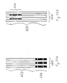
- Fig. 13 shows a multiple quantum well waveguide formed by a plurality 350 of quantum well layers, which are alternatingly made of Al Ga As and GaAs, embedded between two Al Ga s P 1- P q 1-q cladding layers 352 and 354.
- the thickness of each of the quantum well layers is of the order of 20 nm or smaller.
- In the outer boundary of the cladding layer 352 is a circular grating 356 with rectangular ridges.
- the radial width W of the ridges is one quarter of the radial spacing ⁇ of the ridges.
- the spacing ⁇ of about 0.2 micrometers corresponds to the wavelength of the guided wave in the wavelength range, where the multiple quantum well structure can provide optical gain due to pumping with an electron beam.
- Fig. 14 shows a double heterostructure formed by a Ga In As Sb central layer 360 embedded between p 1-P q 1-q two Al Ga As Sb cladding layers 362 and 364.
- the GaInAsSb r 1-r s 1-s central layer is pumped by a short wavelength optical beam.
- the spacing ⁇ of the ridges is equal to the wavelength of amplified guided waves so that laser action occurs at sufficiently strong pumping.
- Fig. 15 shows the coupling of a cladded-core glass fiber 370 to the laser diode 368 according to Fig. 12.
- the fiber is a so-called single mode fiber. This means that it supports only the fundamental waveguide mode at the free space wavelength ⁇ of the laser radiation.
- the fiber is arranged to the monolytic lens 340 such that the beam 372, which is guided by the fiber 370, is coupled as a substantially vertical beam toward the outer part 304 of the ating.
- the polarization of the beam 372 coincides with the polarization of the laser diode output beam 306.
- the beam 372 has a small wavelength offset ⁇ with respect to ⁇ .
- the beam 372 is amplitude or phase modulated.
- the polarization and phase matched beams 306 and 372 leave the resonator through the pin hole 374.
- the pin hole 374 is formed by decreasing the radius of the anti-reflection layer 342 and the inner radius of the contact 314 to the radius of the beam 372.
- the contact layer 342 then also acts as a mirror layer for the rays 306 to the sides of the pin hole 374.
- the thickness of the lower cladding layer 324 is therefore adjusted such that the reflected rays 306 interfere constructively with the rays 307.
- the mirror layers 314 and 316 form then a Fabry-Perot resonator being resonant at the free space resonance wavelength ⁇ of the guided wave resonator.
- the photodiode 376 can detect the beat note of the two beams, thereby realizing the heterodyne detection of the information stream carried by the injected beam 372.
- Fig. 16A and 16B show an arrangement similar to Fig. 12, but without means for circumferential mode selection.
- the grating 378 of the center part 300 remains unchanged. Care is taken to account for a residual difference between the effective refractive indices along the x and y axis.
- the curvature of the grating lines therefore rather follows the curvature of the phase fronts of the standing wave patterns than the curvature of exact circles.
- the means 340 and 346 for rear output coupling are also omitted.
- the contact/mirror layer 316 covers the whole area of the center part 300.
- the beam 306 is then coupled via a transmission medium 380 into a cladded-core multimode fiber 382 with a core radius substantially equal to the radius of the inner part 300.
- the standing wave energy is shared by a plurality of modes with an odd integer number m of radial nodal lines. This results in a more homogeneous energy distribution within the resonator.
- Fig. 17 shows a grating-waveguide configuration similar to Fig. 1 but with a waveguide for surface polaritons.
- the waveguide includes a metal layer which is capable of second harmonic generation, if energized by a high intensity wave.
- the waveguide supports the fundamental pump wave and the second harmonic wave. These fundamental and second harmonic waves are phase matched, which means that the effective refractive index n of the waveguide is substantially equal for eff both waves.
- the grating in this device is both (1) a first order grating providing distributed feedback in a mode with one nodal line for the fundamental wave, and (2) a second order grating providing emission into a linear polarized vertical beam for.the second harmonic wave.
- Fig. 17 shows a cross section of the waveguide structure.
- a glass film 402 (Corning 7059) with a higher refractive index than the substrate.
- the thickness D of the film (about 1 ⁇ m) is adjusted so that the difference of the effective refractive indices for the fundamental wave and the second harmonic wave is as minimal as possible.
- a circular grating 404 In the glass film is formed a circular grating 404.
- a thin Ag layer 406 (5 nm thick).
- the radial width W of the ridges is equal to one half of the radial spacing ⁇ .
- the radial position of the ridges is fine tuned such that the grating lines provide distributed feedback for the fundamental wave for the mode with one circumferential nodal line and with the magnetic field oriented parallel to the layers of the waveguide.
- the pump ray 408 is coupled as a guided wave radially into the resonator.
- the second-harmonic wave generated by the silver layer 406 is coupled into a beam 410, which is linearly polarized perpendicular to the direction of the pump ray 408.
- a photodetector with internal photoemission enhanced by grating coupling to surface plasma waves is shown in Fig. 18.
- a circular . grating 420 with a radial spacing of consecutive ridges 422 and 424 of 2 micrometers and with a width W of the ridges equal to ⁇ /4 is fabricated photolithographically on a heavily doped p-type InP substrate 426.
- the height of the ridges is 0.1 micrometer.
- An electron- beam evaporated Au film 428 is deposited on the grating 420 to form a Schottky barrier.
- the gold film thickness is 50 nm.
- An ohmic contact 430 is thermally evaporated on the backside of the substrate 426.
- a vertical beam 432 with a conical phase front 434 is irradiated along the symmetry axis 436 of the device.
- the irradiated beam 432 has a free space wavelength ⁇ of about 1 micrometer, at which the metal film 428 is normally almost totally reflecting. If the angle of incidence 9 is such that i the interface between the metal 428 and the air can guide a surface plasma wave, the quantum efficiency for the extraction of the photocurrent I is strongly enhanced.
- the axial intensity distribution for this case is illustrated in by the diagram 438. This photodetector configuration is particularly good in attaining pico-second response speed with enhanced quantum efficiency.
- Fig. 19 illustrates a microwave antenna according to the invention providing means with which millimeter waves are transmitted or received.
- the arrangement of Fig. 19 comprises a planar metal dielectric waveguide with a plurality of concentric circular ridges 450 in a highly reflecting metal surface.
- the radial spacing of the ridges (1 mm) is equal to twice the radial width of the ridges and equal to twice the height of the ridges.
- the metal grating is covered'by a dielectric 452 (5 mm thickness) so that the wave energy is essentially confined to this dielectric.
- a coaxial feeder 454 In the center of the waveguide is a coaxial feeder 454, which ends in a circular metal plate 456.
- the distance from the plate 456 to the metal surface is essentially equal to ⁇ /(2n), where ⁇ is the free space operation wavelength and n is the refractive index of the dielectric at the wavelength ⁇ . Below the plate 456 the metal surface is uncorrugated in the region 458, which favors the formation circular wave fronts.
- a millimeter wave is fed through the coaxial waveguide it is coupled into a guided wave with concentric circular wave fronts.
- the ridges scatter the radiation into a beam 460 with generally coaxial wave fronts.
- the wavelength ⁇ /n of the guided wave is substantially equal to the spacing ⁇ of the ridges, the emission occurs into a vertical beam 460.
- the emitted beam can be made linearly polarized, if the wave fed through the coaxial guide has one radial nodal line.
- the beam has a low side lobe level due to the smooth exponential decay in the radial direction of the near field of the antenna.
- Fig. 20 illustrates a rod-shaped microwave antenna according to the invention with which centimeter waves are transmitted or received.
- the arrangement of Fig. 20 comprises an inner circular metal hollow waveguide 470 and an outer circular metal dielectric rod waveguide 472.
- the outer metal surface of the rod carries two sets 474 and 476 of closed loop metal ridges 478. Between the ridges 478 is a wave transmitting dielectric coating 480.
- -In each set the ridges have a constant axial spacing ⁇ (1 cm) and have an axial width W equal to a quarter of the spacing ⁇ .
- the two sets of ridges are axially shifted together by the distance equal to a quarter of the axial spacing4 of the ridges.
- the inner waveguide 470 and the outer waveguide 472 are coupled by a plurality of slits 482.
- the slits have an axial distance ⁇ equal to the axial distance of the ridges.
- the guided waves of the inner waveguide 470 and the outer waveguide 472 are phase matched by an appropriate choice of the thickness of the dielectric coating 480.
- each set 474 and 476 acts as a second order grating.
- a guided wave which is axially outgoing from the center plane 484 is back reflected into an incoming guided wave by the ridges and superimposes in-phase onto the primary outgoing wave, due to the axial shift of the two sets. 474 and 476.
- the axially counter propagating waves are illustrated by the bidirectional rays 486.
- the standing wave pattern due to the two counter-propagating waves is illustrated by the curve 488.
- the curve 488 shows the 2 square H of the circumferentially oriented magnetic field due to the two axially counter-propagating waves along the cylinder axis.
- the intensity decreases exponentially with increasing axial distance from the center plane 484. Therefore, all of the energy is axially trapped if the rod resonator is sufficiently long.
- radiation is emitted vertically. This is illustrated by the rays 490.which lie in planes parallel to the center plane 484.
- the radiation pattern as a function of the angular offset from the vertical direction, is symmetric since the axial nearfield H is symmetric with respect to the center plane 484.
- the emission is essentially equally intense in all radial directions in the plane 484, since the antenna is fed by a waveguide mode without a nodal line.
- the emission characteristic as a function of the angular offset from the vertical direction has a low side lobe level, due to the smooth exponential decay of the axial antenna nearfield.
- FIGS. 21A and 21B show an application of the grating of the inner part 22 in the Figures 1A and 1B to collect electromagnetic radiation. It is proposed to collect radiation energy by a diffraction grating and to transport the energy in a waveguide to a photodetector. There, the optical energy is transformed into electric energy.
- Fig. 21A shows a solar cell 540, which is connected via a matching arrangement 542 (tapered waveguide) to a grating-waveguide configuration 544.
- Fig. 21B shows a top view of a combination of several units according to Fig. 21A.
- the fabrication is carried out on a substrate 546 (glass), which has a surface with optical mirror quality.
- a conducting metal layer 548, an insulating layer 550 and an upper conducting layer 552 are evaporated.
- the upper metal layer 552 and the insulating layer 550 are removed in a circular area.
- an N-type doped polycrystalline silicon layer 554 (1 um thick) is deposited, followed by a P-type doped polycrystalline silicon layer 556 (1 M m thick).
- a ring shaped metal contact 558 (10 um radius) is evaporated. To the sides of the metal contact, the silicon is removed by a mesa etch, whereby a part of the tapered waveguide 542 and the ring-shape of the diode are formed.
- the slopes of the diode are covered with an insulating layer 560 by oxidation of the silicon.
- the ring contact 558 and the lower metal layer 548 are connected by a metal film 562.
- a transparent plastic film 564 (0.6 um thick) is spinned on the reflecting metal surface 564.
- the diffraction grating 566 is transferred to the plastic layer 564 by injection molding of a metal stamper under elevated temperature.
- the grating on the metal stamper is taken from a father grating by electroforming.
- the father grating is fabricated by holographic exposure of photo resist film.
- Fi g. 22 illustrates the holographic method to generate a cylindrical grating.
- a laser beam 568 is irradiated through a conical prism 570 and a liquid 572, which matches.the refractive indices, on a photo resist 574.
- the photo resist film is spinned on the carrier 576 of the father grating.
- the laser beam 568 has planar or conical phase fronts 578 over the crossection of the conical prism 570. Within the conical prism conical phase fronts are formed.
- a system 580 of rings which exposes the photo resist film.
- the radial distance of the rings can be adjusted by varying the wavelength of the irradiated laser light or also by varying the inclination of the conical phase fronts 578 of the irradiated laser light.
- the inclination of the phase fronts 578 can be produced by a further conical prism (not shown), which is inserted into the beam, or by slightly focussing or defocussing of the laser beam 568.
- the grating-waveguide-configuration 544 is optimized for the wavelength range, in which sun light generates the greatest contribution to the photo current i P (wavelengths around 0.5 um).
- the radial distance n of the grating lines is equal to the wavelength of the circular cylindrical wave in the waveguide (2nd order grating) and the grating generates phase reversal for vertically incoming radiation 582.
- the radius (several 100 um) of the diffraction grating should be less than the coupling length of the grating.
- the coupling length of the grating is the length, within which a percentage of 90 % of the intensity of a guided circular cylindrical wave is emitted out of the waveguide.
- the collecting area of the diffraction grating is 100 to 1000 times larger than the area for absorption of radiation in the solar cell.
- the waveguide should have a large numerical aperture, to enable the grating-waveguide-configuration 544 to transmit a relatively large range of wavelengths to the solar cell.
- the electrical energy is collected by the metal layers 548 and 552.
- Fig 21B show a top view of a combination of several units 583 according to Fig. 21A on a common substrate.
- the circular cylindrical gratings are situated at the corners of a regular hexagon (comparable to the arrangement of honey combs), to achieve maximum coverage of the area.
- This matrix of cylindrical diffraction gratings can be fabricated by a single step, if the mentioned father grating is provided with a corresponding matrix of gratings.
- the father grating can be fabricated by repeated exposure of the photo resist 574 film in Fig. 22 through the accordingly displaced conical prism (step repeat method) .
- Fig. 21B In the arrangement according to Fig. 21B, about 70 % of the area is covered by optically collecting gratings.
- the arrangement according to Fig. 23A is similar to Fig. 21A, but it is provided with a solar cell 584 of the form of a stripe (10 ⁇ m width). To the sides of the solar cell there are gratings 586 (width several 100 um). In sector shaped regions (not shown) around the ends of the solar cell stripe, the, grating lines are interrupted, leading to gratings 586 with essentially straight lines.
- the solar cell is provided with metal contacts 588 and 589.
- Fig. 23B shows a top view of a combination of several units according to Fig. 23A on a substrate.
- a diffration grating 586 is oriented toward the cell.
- the collection of the optical energy is illustrated by arrows 587.
- the electrical energy is collected by the contact stripe 590 and the metal film 588.
- the coverage . of the area by the diffraction gratings 586 is increased to over 90 %.
- the area of the collecting diffraction gratings is about 10 to 30 times larger than area for absorption of the radiation within the solar cells.
- the arrangements in the Figures 21 and 23 have the following advantages in comparison to solar cells, which use a lens for collection of the solar energy.
- the efficiency of the solar cells 540 and 584 is relatively high due to the low electrical series resistance (made possible by the large area contacts 558 and 589-covering the solar cell).
- the production costs are relatively low due to the planar technology, which allow mass fabrication.
- FIGS. 24A and 24B illustrate a semiconductor laser diode with distributed feedback and with a loss modulator.
- the emission is spectrally and spatially selective amplified by an arrangement similar to Fig. 1.
- Fig. 24A shows a crossection of the laser with a resonator similar to Fig. 1, but with a circular cylindrical diffraction grating 600, which provides the back reflection and the coupling of energy of the guided wave into the beams 602 and 604.
- the grating is situated in the upper guide layer 606.
- Fig. 24B shows a top view of the grating and has indicated x and y cartesian-coordinates.
- the central layer 608 can amplify or absorb radiation, depending on the excitation.
- the excitation is controlled by the contact segments 610 and 612.
- Fig. 24C illustrates the contact segments 610 and 612. In the center is a circular contact 610.
- the outer region is provided with sector shaped contact segments 612.
- the resonator is built into a luminescent diode, which is excited by a pair of contacts 610 and 614.
- the contact 614 has the form of a ring, to allow the extraction of vertically emitted radiation.
- the contact 610 is acting as a mirror, too.
- the waveguide is formed by a central region 608, which is a multiple quantum well region.
- the quantum wells are formed by alternating Al p Ga 1-p As and GaAs layers.
- the central region 608 is embedded between a P-type doped Al P Ga 1-P As upper confinement layer 606 and a P-type doped Al q Ga 1-q As upper cladding 616 on one side and an N-type doped Al P Ga 1-P As lower confinement layer 618 and an N-type doped Al q Ga 1-q As lower cladding layer 620 on the other side.
- the aluminum mole fractions (p - 0.2 and q - 0.6) of the ternary layers are chosen such that both a super lattice is formed in the central region 608 and the refractive indices of the waveguide layers decrease along the direction from the central region 608 to the cladding layers 616 and 620.
- the grating 600 consists of a plurality of concentric circular boundary displacements forming ridges and grooves in the upper confinement layer 606.
- the top of the ridges in the upper confinement layer 606 is drawn in Fig. 24B in solid black,
- the ridges have substantially vertical side walls.
- the ridges have constant radial width W and radial distance n.
- the radial distance n of the ridges (about 0.25 ⁇ m) is equal to the wavelength in the guide (2nd order grating) at the free space operating wavelength 2.
- the wavelength 2 (about 0.8 um) is determined by the wavelength of maximum amplification of the central region 608 under excitation.
- the radial width W is chosen equal to a quarter of the wavelength in the guide, to maximize the vertical emission of the grating.
- the radial position of the ridges is chosen such that maximum distributed feedback occurs for field distributions with an odd number of radial nodal lines. This fine tuning of the radial position of the ridges has been explained in conjunction with Fig. 4.
- the upper cladding layer 616 and the lower cladding layer 618 are covered by a heavily P-type doped GaAs contact layer 622 and a heavily N-type doped Al-Ga 1-p As contact layer 124.
- the aluminum mole fraction r - 0.2 is chosen such that the layer 624 is transparent for the output beam 602.
- the semiconductor layers are fabricated by a two-step-epitaxy- process.
- the diffraction grating is fabricated essentially by a grating mask written with an electron beam,.and exposure by X-ray lithography.
- Then the remaining semiconductor layers are grown by epitaxy.
- the metal contacts are deposited by evaporation. Finally a window is etched into the substrate for the output beam 602.
- the regions of the active layer 608 below the contact segments 610 and 612 can amplify or absorb radiation, depending on whether the diodes controlled by the contact segments are forward or reverse biased.
- the contact 614 and the contact layer 624 act as common contact for all diode regions.
- the central region 608 emits and amplifies optical radiation. Due to the backreflection of the grating 600, a circular cylindrical standing wave is generated. If enough current is injected, the optical amplification can compensate for the optical losses, and laser action starts.
- the single frequency radiation is coupled into a beam 602 by the grating.
- the relatively large area of the emitting region causes a beam with a narrow radiation lobe (aperture angle smaller 1°).
- Fig. 1 has illustrated the exponential decrease (curve 30) of the intensity in the radial direction due to the action of the grating of the outer region 22. At the slopes of the substrate 626, which form the border of the emitting area, diffracted waves of relatively low intensity are generated. Therefore the beam 602 has a relatively high side lobe suppression.
- the diameter of the active region 608 below the disk contact 610 is nearly equal to the diameter of the volume filled by the optical field.
- the relatively simple laser diode structure has a low threshold current in particular for short wavelength laser radiation, since then the area for current injection can be kept small.
- Fi g. 24C shows schematically the connection of two contact segments 628, which are arranged symmetrically with respect to the center of the grating, to the common contact 614. Due to the irradiation of light, the diode regions below the contact segments 628 have higher absorption than the diode regions below the contact segments 630, which are rotated by 90° with respect to the segments 628. The higher absorption is caused by the extraction of carriers out of the diode regions below the contact segments 628. The carrier extraction leads to the current i.. In the current regions below contact segments without connection to the common contact, the collection of electron-hole-pairs leads to saturable absorption.
- the field energy in the laser resonator is preferentially concentrated in a resonator mode with one radial nodal line parallel to the symmetry line 632 of the contact segments 628.
- the output beam 602 is polarized along the direction of the line 632.
- the direction of polarization can be rotated by 90° by connecting the contact segments 630 instead of the contact segments 628 to the common contact.
- the sector shape is an optimum for circular cylindrical resonators.
- the resonator mode with the'rotated nodal line has the same total loss - and therefore the same quality factor - as the primary resonator mode before the rotation. Intensity and frequency of the laser beam remain essentially constant during the rotation.
- a change of the resonator mode selection also can be achieved by a change of the angular distribution of the optical amplification in the laser resonator (for example by a corresponding radial segmentation of the disk contact 610).
- the important point is to take influence on the quality factors of the resonator modes. To achieve the selection of a particular resonator mode from the ensemble of the possible modes, an increase of its quality factor by a few percent relative to the quality factors of the other modes is sufficient.
- a laser beam with rotary polarization is generated by variation of the angular distribution of the optical losses (or amplification) in the laser resonator.
- the contact segmentation shown in Fig. 24C makes possible the selection of a resonator mode with one radial nodal line. By a proper choice of the angular distribution of the optical losses, resonator modes with several radial nodal lines can be selected.
- the Figures 25A and 25B show other angular distributions of the optical absorption.
- the black drawn areas 634 and 636 illustrate regions with higher absorption. This angular distribution can be achieved for example by a correspondingly larger number of contact segments 612 in Fig. 24A and by corresponding electrical connections.
- the spatial distribution of absorption in Fig. 25A gives the highest quality factor to the resonator mode with one radial nodal line 638 along the y-axis. Therefore, this mode oscillates preferentially.
- the spatial distribution of the losses in Fig. 25B leads to preferential oscillation of the resonator mode with three radial nodal lines 640, which are rotated against each other by 120°.
- the aperture angles ⁇ . of the sectors in the Figures 25A and 25B and the absorption of the sectors is chosen such that both resonator modes have essentially equal quality factors.
- Fig. 26 shows the confinement factor C m of a sector shaped region with absorption versus the aperture angle ⁇ . of the sector for several modes.
- Parameter is the mode index m, which corresponds to the number of radial nodal lines in the intensity distribution of a mode. All considered modes have at least one radial nodal line in the center of the sector of higher absorption (or lower amplification).
- both resonator modes will oscillate simultaneously.
- the angular position and the aperture angle of the sectors are chosen such that both resonator modes have the same quality factor. Switching of the absorbing regions doesn't change significantly the quality factors of lasing modes so that the intensity and the frequency of the laser beam remain essentially constant.
- mode modulation has been illustrated by modes with an odd number of radial nodal lines.
- mode modulation can be realized with modes, which have an even number of radial nodal lines.
- FIGS. 27A and 27B show schematically arrangements of M stripe laser resonators (diode laser array), which are laterally coupled by a thin film waveguide, with integrated absorbers.
- a system of M coupled resonators 650 has at least M resonator modes (super modes).
- the controlled selection of individual resonator modes can be achieved by a proper variation of the amplification in the region 652.
- the absorption between the stripes can be influenced by the regions 654 in Fig. 27B.
- individual or several resonator modes can be excited so that mode modulation is realized.
- Fig. 28 illustrates an example for the transmission of a signal comprising several binary digits.
- the imaging system 662 is formed by a system of lenses, by way of example. Also the use of .a multimode fiber with a mode content adapted to the mode content of the laser beam 660 would be possible.
- the spatially modeselective detector arrangement 664 in Fig. 28 has to be constructed in a different manner, depending on whether the laser beam is analyzed in the Fourier-optic frequency domain or space domain (qualitatively corresponding to the nearfield or the farfield of the laser beam).
- Fig. 29 shows the detector arrangement schematically.
- the signal 666 is mode modulated with M modes by means of a laser according to the Figures 24 and 25.
- the signal 666 is divided between M heterodyne detectors 670 by means of the beam splitters 668.
- Each of the detectors 670 contains a laser 672 (not shown), which oscillates in one of the modes of the signal beam 666.
- the different modes are illustrated in Fig. 29 by a schematic graph of their spatial intensity distribution.
- the lasers 672 are phase locked, as illustrated by the dashed line 676. By this way each detector 670 selects the information transmitted by the corresponding mode.
- the transmitted information is available in the form of M signal values. Due to the modulation technique, the sum of the signal values is essentially constant as a function of time.
- Fig. 30 shows a detector, which realizes spatial mode selection by a single heterodyne detector.
- the mode modulated signal 666 is superimposed polarization matched to a laser beam 682, which is composed of the M modes used for information transmission.
- the spatial mode selection is achieved by segmentation of the detector area 684.
- the detector area can be divided for example into sector shaped regions, with the sectors arranged according to the black drawn sectors in the Figures 25A and 25B.
- Each of the detectable modes is associated with a group of sector shaped detectors, which correspond for example to the group of sectors in the Figures 25A and 25B.
- the group of sectors arranged according to Fig: 25A is used for the detection of the mode with one radial nodal line.
- the group of sectors arranged according to Fig. 25B is used for the detection of the mode with three radial nodal lines. For the detection of higher order modes a correspondingly finer segmentation is chosen.
- phase modulation of the laser light will require broadband components, if higher.data rates are transmitted.
- Lasers can be modulated via the pump rate.
- the resulting modulation of the amplification is often accompanied by a modulation of the refractive index of the active medium, which causes a phase modulation of the laser light.
- phase modulation Apart from slow spurious modulation for example due to variations of temperature or amplification saturation, it is generated phase modulation in the literal sense of the word, which means that the phase deviation A6 is essentially independent of the modulation frequency f m .
- frequency modulation in the literal sense of the word is particular advantageous, provided the spectral amplitude distribution of the signal is uniform.
- Frequency modulation in the literal sens of the word has a frequency deviation Af, which is independent of the modulation frequency f m .
- broadband frequency modulation can be achieved by proper distortion of the signalband of the modulating injection current (pre-emphasis).
- Fig. 31 illustrates schematically a laser with a loss modulator, which is integrated into the resonator.
- the amplifier 700 and the loss modulator 702 are coupled via the wave 704, which is reflected back and forth between the mirrors 706. Therefore, the loss modulation in the modulator 702 leads in the amplifier 700 to a modulation of the amplification.
- the accompanying modulation of the refractive index of the amplifier medium causes a phase angle modulation of the laser light. Apart from slow spurious modulation for example due variations of the temperature, frequency modulation in the literal sense of the word is generated.
- the transferable signal bandwidth is of the order, of the laser modulation bandwidth, which is of the order of the laser resonance frequency f, in a semiconductor laser.
- ⁇ is the coupling factor of the changes of amplification and refractive index in the amplifier 700 (factor of the amplitude-phase-coupling) and ⁇ p is the photon lifetime of the laser mode.
- a modulation of the quality factor of Aq - 1 % yields a frequency deviation Af of about 2.4 GHz independent of the modulation frequency f m , provided the modulation frequency f m . is smaller than the laser resonance frequency f m .
- the semiconductor laser diode described in Fig. 24 operates as laser with intracavity loss modulator, if a modulating voltage u.(t) (t is the time) is applied between the contact segments 628 and the common contact 614 in.Fig. 24C.
- the diode regions below the contacts 628 should be reverse biased.
- Fig. 32 illustrates these operation conditions.
- the modulation of the electric field across the PN-junction of the diodes causes a modulation of the quality factor of the resonator mode.
- the loss modulation of the resonator mode is relatively small, which nevertheless causes a relatively efficient frequency modulation, according to equation (2).
- the influence of the optical field on the modulator (for example saturation of the absorption) is kept small.
- Fi g. 33 shows schematically a laser with a two-dimensional waveguide 720 and a diffraction grating 722 with a quarter- wavelength-shift in the center 724 (quarter wavelength phase- shifted distributed feedback laser).
- the intensity distribution 726 is plotted along the laser axis z.
- the laser is pumped (illustrated by the arrows 730) in the amplifier section 728 over most of its length so that laser radiation 732 is emitted through the waveguide end ports.
- a modulator section 734 which has an absorption coefficient amod or a refractive index nmod externally controllable along the direction of propagation z of the guided wave. Due to the positioning of the modulator 734 in the region of maximum optical field density, the length of the modulator along the z axis can be kept relatively small. By varying the absorption coefficient amod or the refractive index nmod, the laser emission frequency can be tuned or modulated. The relatively small length of the modulator section 734 and the resulting small electrical and thermal capacity makes possible fast modulation.
- a technique has been described for broadband frequency modulation (in the literal sens of the word) of an oscillator by modulation of the quality factor of the resonator mode.
- a quality modulator or a phase modulator have been inserted at appropriate positions into a resonator with distributed feedback.
- Fig. 34 shows the contact of a semiconductor laser similar to the laser diode in Fig. 24, but having the disk contact 610 separated into an inner contact 750 and an outer contact 752.
- the laser current in is injected.
- a constant voltage U and an alternating current imod (t) are applied.
- the laser output signal then consists of short pulses, which are synchroneous with the modulation frequency. Due to the relatively high density of the optical field in the region of the center of the resonator, the switching of the resonator quality factor can be realized by a relatively low modulation current.
- Fig. 35 illustrates a combination of emitters 760 according to Fig. 24 on a common substrate 761.
- the emitters 760 are optically coupled via a thinfilm waveguide by circular cylindrical leaky waves 762 of the resonators.
- the emitters are electrically controllable separately by at least one contact per emitter, which is not common to the emitters 760.
- the optical fields of all emitters can be phase locked by the leaky waves.
- the arrangement in Fig. 35 makes possible the generation of a single frequency laser beam, which can be focussed onto a small spot.
- the laser rays run through a lens 766. This makes possible enhanced stirring of the laser rays.
- Fig. 36 shows a sphere, which consists of a large number of essentially transparent shells 800.
- the shells or the boundaries between the shells are slightly absorbing.
- the shells have an alternatingly higher and lower speed of propagation or an alternatingly higher and lower absorption for the applied waves.
- the arrangement according to Fig. 36 is storing energy of a field of waves, which is irradiated or generated in the center 804, since waves running radially outward (illustrated by the ray 806) are reflected backward to the center 804. Due to the large number of shells 800, the wave can leave the sphere only strongly attenuated.
- the absorption of the waves causes an increase in temperature of the shells 800 so that heat radiation (illustrated by the rays 808) can be coupled out of the sphere.
- the energy of the wave is spread before being transformed into heat in the shells.
- the arrangement avoids local overheating in the center during the generation of the heat radiation.
Landscapes
- Physics & Mathematics (AREA)
- General Physics & Mathematics (AREA)
- Optics & Photonics (AREA)
- Condensed Matter Physics & Semiconductors (AREA)
- Electromagnetism (AREA)
- Engineering & Computer Science (AREA)
- Microelectronics & Electronic Packaging (AREA)
- Diffracting Gratings Or Hologram Optical Elements (AREA)
- Lasers (AREA)
Applications Claiming Priority (4)
| Application Number | Priority Date | Filing Date | Title |
|---|---|---|---|
| US814612 | 1985-12-30 | ||
| US06/814,612 US4743083A (en) | 1985-12-30 | 1985-12-30 | Cylindrical diffraction grating couplers and distributed feedback resonators for guided wave devices |
| DE3611182 | 1986-04-03 | ||
| DE19863611182 DE3611182A1 (de) | 1986-04-03 | 1986-04-03 | Einrichtung zur beeinflussung von wellen, insbesondere von lichtwellen |
Publications (2)
| Publication Number | Publication Date |
|---|---|
| EP0228088A2 true EP0228088A2 (fr) | 1987-07-08 |
| EP0228088A3 EP0228088A3 (fr) | 1990-05-23 |
Family
ID=25842578
Family Applications (1)
| Application Number | Title | Priority Date | Filing Date |
|---|---|---|---|
| EP86118086A Withdrawn EP0228088A3 (fr) | 1985-12-30 | 1986-12-27 | Laser à surface émissive accordable |
Country Status (1)
| Country | Link |
|---|---|
| EP (1) | EP0228088A3 (fr) |
Cited By (10)
| Publication number | Priority date | Publication date | Assignee | Title |
|---|---|---|---|---|
| US4869568A (en) * | 1987-09-29 | 1989-09-26 | Siemens Aktiengesellschaft | Arrangement comprising a planarly extending thin-film waveguide |
| WO1990007133A1 (fr) * | 1988-12-19 | 1990-06-28 | Reserve Bank Of Australia | Reseau de diffraction |
| WO1991003747A1 (fr) * | 1989-09-04 | 1991-03-21 | Commonwealth Scientific And Industrial Research Organisation | Reseau de diffraction et procede de fabrication correspondant |
| WO1993018419A1 (fr) * | 1992-03-12 | 1993-09-16 | Commonwealth Scientific And Industrial Research Organisation | Reseau de diffraction de securite a effets optiques speciaux |
| FR2688637A1 (fr) * | 1991-03-13 | 1993-09-17 | France Telecom | Laser de puissance a emission par la surface et procede de fabrication de ce laser. |
| CN111478179A (zh) * | 2020-05-25 | 2020-07-31 | 长春中科长光时空光电技术有限公司 | 一种垂直腔面发射激光器及其制作方法 |
| CN113687460A (zh) * | 2021-07-29 | 2021-11-23 | 中国工程物理研究院激光聚变研究中心 | 一种边界快速延伸的声波等离子体光栅产生方法 |
| CN115693176A (zh) * | 2022-10-21 | 2023-02-03 | 上海交通大学 | 超薄宽频带卷型吸波结构 |
| CN116315642A (zh) * | 2023-04-17 | 2023-06-23 | 深圳市笨辉光电科技有限公司 | 一种高效太赫兹芯片及太赫兹波发生器 |
| CN116609879A (zh) * | 2023-03-20 | 2023-08-18 | 中国科学院上海微系统与信息技术研究所 | 一种片外光发射器件 |
Family Cites Families (2)
| Publication number | Priority date | Publication date | Assignee | Title |
|---|---|---|---|---|
| US3725809A (en) * | 1971-04-05 | 1973-04-03 | Bell Telephone Labor Inc | Dielectric ring lasers using waveguiding |
| IT1103647B (it) * | 1978-08-07 | 1985-10-14 | Rignini Giancarlo | Lenti geodetiche perfette per guide d'onda e dispositivo per elaborazione di segnali unidimensionali impiegante dette lenti |
-
1986
- 1986-12-27 EP EP86118086A patent/EP0228088A3/fr not_active Withdrawn
Cited By (13)
| Publication number | Priority date | Publication date | Assignee | Title |
|---|---|---|---|---|
| US4869568A (en) * | 1987-09-29 | 1989-09-26 | Siemens Aktiengesellschaft | Arrangement comprising a planarly extending thin-film waveguide |
| WO1990007133A1 (fr) * | 1988-12-19 | 1990-06-28 | Reserve Bank Of Australia | Reseau de diffraction |
| AU633862B2 (en) * | 1988-12-19 | 1993-02-11 | Reserve Bank Of Australia | Diffraction grating |
| WO1991003747A1 (fr) * | 1989-09-04 | 1991-03-21 | Commonwealth Scientific And Industrial Research Organisation | Reseau de diffraction et procede de fabrication correspondant |
| US5548610A (en) * | 1991-03-13 | 1996-08-20 | France Telecon | Surface-emitting power laser and process for fabricating this laser |
| FR2688637A1 (fr) * | 1991-03-13 | 1993-09-17 | France Telecom | Laser de puissance a emission par la surface et procede de fabrication de ce laser. |
| WO1993018419A1 (fr) * | 1992-03-12 | 1993-09-16 | Commonwealth Scientific And Industrial Research Organisation | Reseau de diffraction de securite a effets optiques speciaux |
| CN111478179A (zh) * | 2020-05-25 | 2020-07-31 | 长春中科长光时空光电技术有限公司 | 一种垂直腔面发射激光器及其制作方法 |
| CN113687460A (zh) * | 2021-07-29 | 2021-11-23 | 中国工程物理研究院激光聚变研究中心 | 一种边界快速延伸的声波等离子体光栅产生方法 |
| CN113687460B (zh) * | 2021-07-29 | 2023-06-06 | 中国工程物理研究院激光聚变研究中心 | 一种边界快速延伸的声波等离子体光栅产生方法 |
| CN115693176A (zh) * | 2022-10-21 | 2023-02-03 | 上海交通大学 | 超薄宽频带卷型吸波结构 |
| CN116609879A (zh) * | 2023-03-20 | 2023-08-18 | 中国科学院上海微系统与信息技术研究所 | 一种片外光发射器件 |
| CN116315642A (zh) * | 2023-04-17 | 2023-06-23 | 深圳市笨辉光电科技有限公司 | 一种高效太赫兹芯片及太赫兹波发生器 |
Also Published As
| Publication number | Publication date |
|---|---|
| EP0228088A3 (fr) | 1990-05-23 |
Similar Documents
| Publication | Publication Date | Title |
|---|---|---|
| US4743083A (en) | Cylindrical diffraction grating couplers and distributed feedback resonators for guided wave devices | |
| US5365541A (en) | Mirror with photonic band structure | |
| KR100229051B1 (ko) | 수직적으로 통합된 광학펌프를 갖는 장파장수직 공동표면 방출레이저 | |
| US5349602A (en) | Broad-area MOPA device with leaky waveguide beam expander | |
| US4957337A (en) | Optical quantum interference device and method of modulating light using same | |
| US6975664B1 (en) | Article comprising a two-dimensional photonic crystal coupler and method of making the same | |
| JP2692913B2 (ja) | グレーティング結合型表面発光レーザ素子およびその変調方法 | |
| US4935930A (en) | Laser light source for generating beam collimated in at least one direction | |
| US20040105476A1 (en) | Planar waveguide surface emitting laser and photonic integrated circuit | |
| EP0862818B1 (fr) | Recepteur heterodyne indirect pour des radiations sous-millimetriques et methode | |
| CN105591284B (zh) | 光栅辅助的微柱腔面发射激光器 | |
| EP0300790B1 (fr) | Laser à semi-conducteur | |
| US4869568A (en) | Arrangement comprising a planarly extending thin-film waveguide | |
| JPH04276682A (ja) | 半導体レーザとそれを有する装置とその製造方法 | |
| US4745607A (en) | Interlayer directional coupling in antiresonant reflecting optical waveguides | |
| Pillai et al. | Paraxial-misalignment insensitive external-cavity semiconductor-laser array emitting near-diffraction limited single-lobed beam | |
| EP0228088A2 (fr) | Laser à surface émissive accordable | |
| US20240380178A1 (en) | Reflector for vcsel | |
| EP0533475B1 (fr) | Dispositif semi-conducteur optique, méthode de production et dispositif laser utilisant des dispositifs semi-conducteur optiques | |
| US4897844A (en) | Information transmission by mode modulation and laser oscillators thereof | |
| KR20050107439A (ko) | 주파수 변환장치 및 변환방법 | |
| EP0560474A2 (fr) | Réseau 2-D à laser à semi-conducteur cohérent monolithique | |
| CN111600199B (zh) | 一种有限长带宽的高功率半导体激光器 | |
| Park et al. | Optical sensing by using photonic quantum ring lasers and resonance-enhanced photodetectors | |
| JP3269584B2 (ja) | 光子バンド構造を備えたミラーを使用するレーザ・アレイ結合 |
Legal Events
| Date | Code | Title | Description |
|---|---|---|---|
| PUAI | Public reference made under article 153(3) epc to a published international application that has entered the european phase |
Free format text: ORIGINAL CODE: 0009012 |
|
| AK | Designated contracting states |
Kind code of ref document: A2 Designated state(s): DE FR GB IT NL SE |
|
| PUAL | Search report despatched |
Free format text: ORIGINAL CODE: 0009013 |
|
| AK | Designated contracting states |
Kind code of ref document: A3 Designated state(s): DE FR GB IT NL SE |
|
| 17P | Request for examination filed |
Effective date: 19901123 |
|
| 17Q | First examination report despatched |
Effective date: 19911212 |
|
| RAP3 | Party data changed (applicant data changed or rights of an application transferred) |
Owner name: SCHIMPE, ROBERT MICHAEL, DR. |
|
| STAA | Information on the status of an ep patent application or granted ep patent |
Free format text: STATUS: THE APPLICATION IS DEEMED TO BE WITHDRAWN |
|
| 18D | Application deemed to be withdrawn |
Effective date: 19950701 |