EP0533475B1 - Dispositif semi-conducteur optique, méthode de production et dispositif laser utilisant des dispositifs semi-conducteur optiques - Google Patents
Dispositif semi-conducteur optique, méthode de production et dispositif laser utilisant des dispositifs semi-conducteur optiques Download PDFInfo
- Publication number
- EP0533475B1 EP0533475B1 EP92308484A EP92308484A EP0533475B1 EP 0533475 B1 EP0533475 B1 EP 0533475B1 EP 92308484 A EP92308484 A EP 92308484A EP 92308484 A EP92308484 A EP 92308484A EP 0533475 B1 EP0533475 B1 EP 0533475B1
- Authority
- EP
- European Patent Office
- Prior art keywords
- layer
- light
- semiconductor
- light guide
- optical semiconductor
- Prior art date
- Legal status (The legal status is an assumption and is not a legal conclusion. Google has not performed a legal analysis and makes no representation as to the accuracy of the status listed.)
- Expired - Lifetime
Links
Images


Classifications
-
- G—PHYSICS
- G02—OPTICS
- G02B—OPTICAL ELEMENTS, SYSTEMS OR APPARATUS
- G02B6/00—Light guides; Structural details of arrangements comprising light guides and other optical elements, e.g. couplings
- G02B6/10—Light guides; Structural details of arrangements comprising light guides and other optical elements, e.g. couplings of the optical waveguide type
- G02B6/12—Light guides; Structural details of arrangements comprising light guides and other optical elements, e.g. couplings of the optical waveguide type of the integrated circuit kind
- G02B6/122—Basic optical elements, e.g. light-guiding paths
- G02B6/124—Geodesic lenses or integrated gratings
-
- H—ELECTRICITY
- H01—ELECTRIC ELEMENTS
- H01S—DEVICES USING THE PROCESS OF LIGHT AMPLIFICATION BY STIMULATED EMISSION OF RADIATION [LASER] TO AMPLIFY OR GENERATE LIGHT; DEVICES USING STIMULATED EMISSION OF ELECTROMAGNETIC RADIATION IN WAVE RANGES OTHER THAN OPTICAL
- H01S5/00—Semiconductor lasers
- H01S5/02—Structural details or components not essential to laser action
- H01S5/026—Monolithically integrated components, e.g. waveguides, monitoring photo-detectors, drivers
-
- H—ELECTRICITY
- H01—ELECTRIC ELEMENTS
- H01S—DEVICES USING THE PROCESS OF LIGHT AMPLIFICATION BY STIMULATED EMISSION OF RADIATION [LASER] TO AMPLIFY OR GENERATE LIGHT; DEVICES USING STIMULATED EMISSION OF ELECTROMAGNETIC RADIATION IN WAVE RANGES OTHER THAN OPTICAL
- H01S5/00—Semiconductor lasers
- H01S5/10—Construction or shape of the optical resonator, e.g. extended or external cavity, coupled cavities, bent-guide, varying width, thickness or composition of the active region
- H01S5/12—Construction or shape of the optical resonator, e.g. extended or external cavity, coupled cavities, bent-guide, varying width, thickness or composition of the active region the resonator having a periodic structure, e.g. in distributed feedback [DFB] lasers
- H01S5/1228—DFB lasers with a complex coupled grating, e.g. gain or loss coupling
-
- H—ELECTRICITY
- H01—ELECTRIC ELEMENTS
- H01S—DEVICES USING THE PROCESS OF LIGHT AMPLIFICATION BY STIMULATED EMISSION OF RADIATION [LASER] TO AMPLIFY OR GENERATE LIGHT; DEVICES USING STIMULATED EMISSION OF ELECTROMAGNETIC RADIATION IN WAVE RANGES OTHER THAN OPTICAL
- H01S5/00—Semiconductor lasers
- H01S5/40—Arrangement of two or more semiconductor lasers, not provided for in groups H01S5/02 - H01S5/30
- H01S5/4025—Array arrangements, e.g. constituted by discrete laser diodes or laser bar
-
- H—ELECTRICITY
- H01—ELECTRIC ELEMENTS
- H01S—DEVICES USING THE PROCESS OF LIGHT AMPLIFICATION BY STIMULATED EMISSION OF RADIATION [LASER] TO AMPLIFY OR GENERATE LIGHT; DEVICES USING STIMULATED EMISSION OF ELECTROMAGNETIC RADIATION IN WAVE RANGES OTHER THAN OPTICAL
- H01S5/00—Semiconductor lasers
- H01S5/50—Amplifier structures not provided for in groups H01S5/02 - H01S5/30
Definitions
- the present invention generally relates to optical semiconductor devices, and more particularly to an optical semiconductor device having a periodic layer structure. Further, the present invention is concerned with a method of producing such an optical semiconductor device, and a laser device using optical semiconductor devices as described above.
- semiconductor materials have respective inherent bandgaps and refractive indexes.
- a semiconductor material has the function of absorbing light having a wavelength equal to or less than the bandgap thereof.
- An optical confinement effect takes place by surrounding a semiconductor material having a high refractive index by another semiconductor material having a low refractive index. By utilizing the optical confinement effect, an optical waveguide structure can be configured.
- a periodic structure in which the refractive index varies periodically in a light propagation direction of light functions as a grating.
- grooves are photolithographically formed at fixed intervals (a fixed period) on a surface of a substrate or a buffer layer formed on the substrate.
- a semiconductor layer having a refractive index different from that of the substrate or the buffer layer is formed on the surface thereof so that the grooves are buried by the semiconductor layer.
- a waveguide is formed on the semiconductor layer.
- An optical semiconductor device thus formed functions as a grating.
- a direct-transition-type semiconductor uses a luminescent recombination effect by injecting current into the semiconductor.
- the intrinsic layer of a pin diode is made of a direct-transition type semiconductor, and a resonator structure having the above pin diode structure serves as a semiconductor laser.
- a distributed-feedback (DFB) laser structure having a fixed oscillation wavelength can be made by a combination of a semiconductor laser and a grating.
- the grating functions as a selective mirror with respect to light having the fixed oscillation wavelength, and oscillates with a wavelength in which light portions reflected by grooves of the grating are in phase with each other.
- semiconductor materials function as not only passive optical media having respective fixed refractive indexes and but also as light-absorbing media and light-emitting media.
- the optical semiconductor device comprises first and second cladding layers and a light guide structure sandwiched between the first and second cladding layers; in which the light guide structure has a layer structure including a first layer, a second layer and a third layer, a plurality of grooves being formed periodically on the surface of the first layer, the second layer being formed on at least parts of these grooves with a refractive index larger than that of the first layer and the third layer, having a refractive index smaller than that of the second layer, being formed on the second layer, whereby the structure has a periodic variation in refractive index in a predetermined direction, and a second periodic variation in optical gain in the predetermined direction, the first and second periodic variations having identical periods but having a phase difference such that the structure shows a first reflection factor with respect to light incoming from the left side thereof, and a second reflection factor with respect to light having the same properties as the light incoming from the left side, but incoming from the right side thereof, the first and second reflection factors being different from
- JP-A-3058410 describes a method of manufacture of quantum fine wires.
- AlGaAs is grown on a GaAs substrate, grooves are formed in the AlGaAs and then GaAs is grown by molecular beam epitaxy in which a beam is obliquely projected onto the grooves. This forms GaAs fine wires in the grooves.
- AlGaAs is then grown over the surface.
- a not dissimilar method is used to produce the desired phaseoffset structures.
- the method according to claim 21 comprises the steps of: (a) forming a first layer on a base, the first layer serving as one of a light guide layer, and an active layer; (b) forming a plurality of grooves on a surface of the first layer; (c) obliquely projecting a gas onto the surface of the first layer so that a second layer having a refractive index larger than that of the first layer is formed on the grooves; and (d) forming a third layer on the second layer, the third layer having a refractive index smaller than that of the second layer, the third layer serving as either an active layer or a light guide layer.
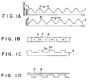
- Figs. 1A through 1D show an optical semiconductor device according to a first embodiment of the present invention.
- Fig. 1A is a graph schematically illustrating the structure of the optical semiconductor device according to the first embodiment
- Figs. 1B and 1C respectively show layer structures having a periodic variation in refractive index
- Fig. 1D is a diagram schematically showing a layer structure having a periodic variation in optical gain.
- the semiconductor device includes a layer structure having a periodic variation in the refractive index n and a periodic variation in the gain g, and there is a phase difference ⁇ between these periodic variations.
- the periodic index variation has a period p
- the periodic gain variation has the same period p as that of the periodic index variation.
- the refractive index n is an effective refractive index which light senses.
- the periodic index variation shown in Fig. 1A can be made by a periodic layer structure as shown in Figs. 1B and 1C. As shown in Fig. 1B, layers 3 made of a high-index material and layers 4 made of a low-index material are alternately arranged with a fixed period.
- Fig. 1C shows an alternate periodic structure which has the periodic index variation shown in Fig. 1A.
- the structure shown in Fig. 1C is made of an optical medium having a given refractive index, and has thick portions 5a and thin portions which are alternately arranged.
- the periodic gain variation shown in Fig. 1A can be made by a periodic structure as shown in Fig. 1D.
- a layer 8 is made of a medium having no gain. Grooves are periodically formed on a surface of the layer 8.
- a layer 6 made of a medium having a gain is formed on the surface of the layer 8.
- the layer 6 has thick portions and thin portions alternately arranged at a period. The thick portions of the layer 6 have high effective gains, and thin portions thereof have low effective gains. It is possible to form the thin portions with a medium having no gain. It is also possible to form the layer 6 with a light absorbing material having a negative gain (which is lower than a gain of 1). It is necessary to excite the periodic structure shown in Fig. 1D by an exciting means in order to make the layer 6 have an effective gain.
- the exciting means is, for example, injection current, a ray or an electromagnetic wave.
- phase difference ⁇ between the periodic index variation and the periodic gain variation results in the following characteristics.
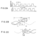
- Figs. 2A, 2B and 2C relate to a structure in which a periodic variation in the refractive index n and a periodic variation in the gain g are formed in an optical waveguide and have identical pitches ⁇ , the phase difference therebetween being equal to ⁇ /4. More particularly, Fig. 2A shows distributions of the refractive index n and the gain g as a function of position in the optical waveguide.
- the refractive index n is a real part of a complex refractive index
- the gain g is an imaginary part thereof. Reflection of light takes place at an interface of the refractive index n or an interface of the gain g.
- a reflection factor r12 of light incident on the medium m2 from the medium m1 is written as: r12 ⁇ - ⁇ n/n 2
- a reflection factor r21 of light incident on the medium m1 to the medium m2 is written as: r21 ⁇ ⁇ n/n 2 .
- a reflection factor r23 of light incident on a medium m2 having an optical gain to a medium m3 is written as: r23 ⁇ -j ⁇ g/n 2 and a reflection factor r32 of light incident on the medium m3 from the medium m2 is written as: r32 ⁇ j ⁇ g/n 2 .
- Fig. 2B is a diagram for schematically explaining reflection taking place when light enters the structure shown in Fig. 2A from the left side thereof
- Fig. 2C is a diagram for schematically explaining reflection taking place when light enters the structure shown in Fig. 2A from the right side thereof.
- the light 13 is reflected by the interface 11 of the refractive index, and a reflected wave 14 having an inverted version of the phase of the light 13 is generated.
- the light reaches the interface 12 of gain, at which a reflected wave 15 which is ⁇ /4 out of phase with the light 13 is generated.
- the reflected wave 15 generated at the interface 12 of gain is reciprocated along an optical path of ⁇ /8, and a phase delay correspnding to ⁇ /4 is generated. Meanwhile the phase of the reflected wave 15 has been shifted by ⁇ /4 when it is reflected by the interface 12.
- the reflected wave 15 when the reflected wave 15 returns to the interface 11 of refractive index, the total phase change is equal to zero, and the reflected wave 15 is 180° out of phase with the reflected wave 14 generated at the interface 11 of refractive index. In this manner, the reflected waves 14 and 15 are canceled.
- a reflected wave 17 having a phase delay of ⁇ /4 is generated from the light 16 at the interface 12 of gain, and a reflected wave 18 in phase with the light 16 is generated at the interface 11 of refractive index.
- the reflected waves 17 and 18 are positively added to each other, and a composite reflected light is generated.
- the structure shown in Fig. 2A shows a first reflection factor with respect to light incoming from the left side thereof, and a second reflection factor with respect to light incoming from the right side thereof, the first and second reflection factors being different from each other.
- the reflection factor obtained at the interface of refractive index is equal to that obtained at the interface of gain, one of the reflected waves is zero.
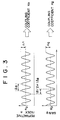
- the horizontal axis z indicates a direction in which light is propagated.
- a variation in the refractive index n has periodicity of a sine wave having an invariant component n D and a spatial variation amplitude ⁇ n around the invariant component n D .
- a variation in the gain g has periodicity of a sine wave having an invariant component g D and a spatial variation amplitude ⁇ g around the invariant component g D .
- n n D + ⁇ n ⁇ cos ⁇ (2 ⁇ / ⁇ B )z + ⁇ where ⁇ denotes an initial phase of the periodic index variation.
- Fig. 4 which shows a modeled resonator having a length L
- Each of the factors in the F-matrix can be obtained by solving the equations (4) and (5) as follows:
- F 11 [cosh( ⁇ L)+ ⁇ (g D -j ⁇ )L/( ⁇ L) ⁇ sinh( ⁇ L)]e -j ⁇ oL
- F 12 ⁇ (K - L)/(j ⁇ L) ⁇ sinh( ⁇ L)e -j( ⁇ oL+ ⁇ )
- F 21 ⁇ (K + L)/(j ⁇ L) ⁇ sinh( ⁇ L)e j( ⁇ oL+ ⁇ )
- F 22 [cosh( ⁇ L)+ ⁇ (g D -j ⁇
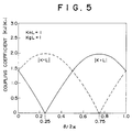
- Fig. 5 is a graph of the ⁇ dependence of the coupling coefficients K + and K - .
- the phase difference ⁇ between the periodic index variation and the periodic gain variation is equal to 3 ⁇ /2.
- one of the coupling coefficients K n and K g is equal to zero when the phase difference is equal to 1/4 or 3/4 the identical periods of the periodic variations in the refractive index and the gain.
- the coupling coefficients of the forward wave have values different from those of the coupling coefficients of the backward wave.
- the coupling coefficients K n and K g are the same as each other.
- the above-mentioned periodic structure functions as a reflector.
- the intensity of light can be amplified since the periodic structure has a gain, and the periodic structure functions as a directional-reflection amplifier.
- the periodic index variation and the periodic gain variation can be made by forming a grating in a semiconductor structure and forming a medium structure which is located within or in the vicinity of the grating and which has a refractive index or gain different from that of the grating.
- Fig. 8A is a cross-sectional view of the layer structure of the optical semiconductor device according to the first embodiment of the present invention.
- Fig. 8B is a graph of a gain distribution of the optical semiconductor device, and
- Fig. 8C is a graph of a refractive index distribution thereof.
- a light guide layer 22 is epitaxially grown on a cladding layer 21 formed with an n-type InP substrate by a MOCVD or MBE process.
- the light guide layer 22 is made of intrinsic InGaAsP having a bandgap wavelength of approximately 1.0 - 1.1 ⁇ m.
- the surface of the i-type light guide layer 22 is photolithographically etched so that grooves are periodically arranged. In this manner, a grating is formed.
- a high-index layer 24 is selectively grown on one of the sidewalls of each groove formed in the light guide layer 23.
- the high-index layer 24 is formed on the right side of each groove.
- the high-index layer 24 is made of intrinsic GaAs having a refractive index higher than that of InGaAsP.
- the selective growth of the high-index layer 24 by the MOCVD or MBE can be made by obliquely supplying a gas to the surface of the i-type light guide layer 22 in order to form the high-index layer 24.
- the surface of the grating with the high-index layer 24 grown thereon is buried by an active layer 25, which is made of intrinsic InGaAs having a bandgap wavelength of approximately 1.5 ⁇ m or 1.3 ⁇ m
- a light guide layer 26 made of intrinsic InGaAsP having a bandgap approximately equal to that of the i-type light guide layer 22 is grown on the surface of the active layer 25.
- a cladding layer 27 made of p-type InP is epitaxially grown on the i-type light guide layer 26. The period of the grating corresponds to 1/2 the wavelength ⁇ of light emitted from the active layer 25.
- the grating is formed on the surface of the light guide layer 22, and the high-index layer 24 is formed so that it is deposited on one side (left side in Fig. 8A) of each of the grooves formed in the light guide layer 22.
- the active layer 25 is also formed so that it is deposited on one side (right side in Fig. 8A) of each of the grooves of the light guide layer 22.
- the active layer 25 When current is made to flow into the optical semiconductor device from the p-type side electrode 29 to the n-type side electrode 28, the active layer 25 functions as a gain layer. As shown in Fig. 8B, the gain layer 25 has a periodic gain variation. The period of the periodic gain variation is the same as the period of the grating.
- the refractive index distribution has a periodic variation, as shown in Fig. 8C. It can be seen from Fig. 8C that the period of the periodic variation in the refractive index n (equivalent refractive index n eq ) is identical to that of the periodic variation in the gain g shown in Fig. 8B.
- the phase difference ⁇ due to the positions of the high-index layer 24 and the active layer 25 with respect to the projections of the i-type light guide layer 22 is made between the periodic index variation and the periodic gain variation.
- the optical semiconductor device shown in Fig. 8A functions as an optical amplifier having different reflection factors.
- Fig. 9 is a cross-sectional view of an optical semiconductor device according to a second embodiment of the present invention.
- An i-type light guide layer 22 made of i-type InGaAsP having a bandgap wavelength of approximately 1.0 - 1.1 ⁇ m is epitaxially grown to a thickness of, for example, 200 nm on the cladding layer 21 made of i-type InP.
- a grating 23a having a sawtooth-shaped cross section is formed on the surface of the i-type light guide layer 22a.
- the right-side wall of each groove of the grating is a gradual slope, and the left-side wall thereof is a vertical surface which stands perpendicular to the layer plane.
- the pitch of the grating is equal to, for example, 202.2 nm, and the depth thereof is equal to, for example, 50 nm.
- a gas is supplied to the surface of the grating 23a from the upper right side thereof in order to grow GaAs so that a GaAs high-index layer 24a having a thick portion on the left side of each groove is formed.
- the high-index layer 24a also functions as a grating.
- an active layer 25a made of i-type InGaAsP having a bandgap wavelength of approximately 1.5 ⁇ m is grown on the high-index layer 24a.
- the aforementioned i-type light guide layer 26 made of i-type InGaAsP having a bandgap of approximately 1.0 - 1.1 ⁇ m, and the p-type cladding layer 27 made of p-type InP are formed in the aforementioned manner.
- the light guide layer 26 is, for example, 0.16 ⁇ m thick
- the active layer 25a is, for example, 0.14 ⁇ m thick.
- the grating is formed so that it has an asymmetrical cross-section, which makes it easy to obtain the phase difference ⁇ between the periodic variations in the refractive index and gain.
- Fig. 10 is a cross-sectional view of an optical semiconductor device which is not an embodiment of the present invention.
- a grating 31 is formed on a surface of a cladding layer 21a formed with an n-type InP substrate, and a semiconductor light absorption layer 32 made of InGaAs is put to one side of each groove formed on the surface of the cladding layer 21a.
- a light guide layer 33 made of i-type InGaAsP is formed on the surface of the device, and an active layer 25c made of i-type InGaAsP is formed on the surface of the light guide layer 33.
- the p-type cladding layer 27 made of p-type InP is formed on the surface of the active layer 25c.
- the n-type side electrode 28 is formed on the surface of the n-type cladding layer 21a, and the p-type side electrode 29 is formed on the surface of the p-type cladding layer 27.
- the active layer 25c of the above device has a uniform thickness and hence a fixed gain.
- the semiconductor light absorption layer 32 formed on the surface of the grating 31 has a periodic structure. Hence, the sum of the gain (plus) of the active layer 25c and the gain (minus) of the semiconductor light absorption layer 32 shows a periodic gain variation.
- the semiconductor light absorption layer 32 has a refractive index higher than that of the light guide layer 33, which has a refractive index higher than that of the cladding layer 21a. That is, the refractive indexes of the layers 32 and 33 are higher than that of the cladding layer 21a, and thereby a periodic index variation can be made.
- the periodic gain variation indicates a high gain value in an area which does not have the semiconductor light absorption layer 32.
- the periodic index variation indicates a high gain value in an area which has the semiconductor light absorption layer 32. Hence, there is the phase difference between the periodic gain variation and the periodic index variation.
- Fig. 11 is a cross-sectional view of an optical semiconductor device according to a third embodiment of the present invention.
- An i-type light guide layer 22a which is made of i-type InGaAsP and has a uniform thickness, is formed on the n-type cladding layer 21 made of n-type InP.
- An active layer 25d which is made of i-type InGaAsP and has a bandgap narrower than that of the i-type light guide layer 22a, is formed on the i-type light guide layer 22a.
- a grating 35 is formed on the surface of the active layer 25d.
- a high-index layer 24b made of i-type GaAs is formed so that it is put to one side (right side in Fig.
- An i-type light guide layer 26a made of i-type InGaAsP is formed so that it buries the grooves of the grating.
- the p-type cladding layer 27 is formed on the i-type light guide layer 26a.
- the n-type side electrode 28 is formed on the surface of the n-type cladding layer 21, and the p-type side electrode 29 is formed on the surface of the p-type cladding layer 27.
- the grating 35 is formed on the active layer 25d, which has a thickness distribution. That is, the active layer 25d has a periodic gain variation.
- the high-index layer 24 is put to one side of each groove of the grating 35, and hence a periodic index variation is obtained.
- Fig. 12A is a block diagram of a long-wavelength laser device using one of the aforementioned optical semiconductor devices.
- Two directional-reflection amplifiers 42 and 43 are coupled to respective ends of an optical fiber 41 having an arbitrary length.
- the directional-reflection amplifier 42 has a fixed reflection factor with respect to light 44 propagated from the right side of the optical fiber 41 to the left side thereof, and emits light 45.
- the directional-reflection amplifier 42 has a reflection factor of approximately zero with respect to the reflected light 45 propagated from the left side of the optical fiber 41 to the right side thereof, and hence returns it to the optical fiber 41.
- the directional-reflection amplifier 42 has a fixed reflection factor with respect to light 47 propagated from the left side of the optical fiber 41 to the right side thereof, and emits light 48.
- the directional-reflection amplifier 43 has a fixed reflection factor of approximately zero with respect to the reflected light 48 propagated from the right side of the optical fiber 41 to the left side thereof, and hence returns it to the optical fiber 41.
- the directional-reflection amplifiers 42 and 43 respectively function to amplify light when a forward current flows into the respective pin structures.
- an optical system including the optical fiber 41 and the directional-reflection amplifiers 42 and 43 form an optical resonator having a gain, and functions as a semiconductor laser device. As the length of the optical fiber 41 increases, the spectrum width of a generated light beam is narrowed.
- Fig. 12B is a block diagram of a directional ring laser, which comprises directional-reflection amplifiers 51 and 52 coupled by optical fibers 53 and 54 so that a loop-shaped waveguide is formed.
- the directional-reflection amplifier 51 has a reflection factor of approximately zero with respect to light 55 propagated from the left side thereof to the right side thereof, and a high reflection factor with respect to light 56 propagated from the right side to the left side.
- light emitted from the directional-reflection amplifier 51 is propagated through the optical fiber 54.
- the light reaches the directional-reflection amplifier 52 via the optical fiber 54, and moves in the directional-reflection amplifier 52 as light 58 propagated from the right side of the amplifier 52 to the left side thereof.
- the directional-reflection amplifier 52 has a reflection factor of approximately zero with respect to the light 58, and has a high reflection factor with respect to light 59 propagated from the left side to the right side. Hence, only the light 58 is amplified and output to the optical fiber 53. In this manner, the light propagated through the loop-shaped waveguide in the clockwise direction serves as a progressive wave and is amplified by the directional-reflection amplifiers 51 and 52. The backward waves 56 and 59 propagated in the counterclockwise direction are reflected by the directional-reflection amplifiers 51 and 52 with a high reflection rate, and are then converted into the progressive waves. An optical waveguide 60 is optically coupled to the optical fiber 54. In the above manner, the laser device shown in Fig. 12B is of a progressive-wave type, in which a strong interaction between modes is obtained because of non-existence of standing waves. Hence, the progressive-wave type laser device is liable to oscillate in a single mode.
- Fig. 13A is a block diagram of a branching and amplifying device according to a fourth embodiment of the present invention.
- Two semiconductor waveguides 112 and 114 intersect at an angle of 90° so that a T-shaped waveguide is formed.
- Each of the semiconductor waveguides 112 and 114 comprises a light guide layer sandwiched between two cladding layers.
- the light guide layer at an intersecting portion 116 of the T-shaped branching waveguide includes a high-index layer and an active layer, which layers are stacked.
- a grating 118 is formed in the high-index layer so that the thickness of the high-index layer periodically varies.
- Another grating 120 is formed in the active layer so that the thickness of the active layer periodically varies.
- the gratings 118 and 120 are obliquely formed at an angle equal to ⁇ /4 with respect to the light propagating direction indicated by an arrow in Fig. 13A, and have identical periods. Further, the phase difference ⁇ between the gratings 118 and 120 is equal to, for example 3 ⁇ /2.
- Fig. 13B is a graph showing a variation in the refractive index n and a variation in the gain g with respect to a cross section taken along line A-A' shown in Fig. 13A. It will be noted that the graph shown on the upper side of Fig. 13B is the same as the graph shown on the upper side of Fig. 3. Due to the periodic variation in the thickness of the high-index layer caused by the grating 118, obtained is a periodic index variation having periodicity of a sine wave having a wavelength ⁇ B ( > ⁇ ) and a spatial variation amplitude ⁇ n around an invariant component n D of the refractive index n. The graph shown the lower side of Fig. 13B is the same as the graph shown on the lower side of Fig.
- the intersecting portion 116 operates as follows when the gratings 118 and 120 are arranged at an angle equal to ⁇ /4 with respect to the light propagating direction indicated by the arrow shown in Fig. 13A.
- the reflection factor R L and the transmittance T L with respect to light incident on the intersecting portion 116 from the right side of the waveguide 112 are respectively equal to 0 and 1.
- the light passes through the intersecting portion 116 and is propagated through the waveguide 112 on the left side thereof. It is to be noted that the light from the right side of the intersecting portion 116 does not branch into the waveguide 114.
- light propagated through the waveguide from the right side branches into the waveguide 114, and passes through the intersecting portion 116.
- the light branching and amplifying operations are concurrently carried out.
- Light propagated through the waveguide 112 on the left side passes through the intersecting portion 116 and is propagated through the waveguide 112 on the right side.
- Fig. 15 is a perspective view of the above-mentioned T-shaped type light branching and amplifying device
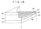
- Fig. 16 is a partially cutaway view of the intersecting portion 116 shown in Fig. 14A
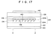
- Fig. 17 is a cross-sectional view taken along the line A-A' shown in Fig. 16.
- a T-shaped ridge is formed on an n-type InP substrate 122.
- a light guide layer 124 made of InGaAsP, and a cladding layer 126 made of p-type InP are formed in an upper portion of the ridge.
- An intersecting portion 132 of the semiconductor waveguides 128 and 130 comprises a GaAs high-index layer 134 and an InGaAsP active layer 136, which layers are stacked and sandwiched between an InGaAsP lower light guide layer 124a which is a part of the guide layer 124 and an InGaAsP upper light guide layer 124b which is another part of the guide layer 124.
- a sawtooth-shaped grating 138 having periodicity of a wavelength ⁇ B is formed at an interface between the high-index layer 134 and the light guide layer 124a in such a manner that the grating 138 is oriented at an angle equal to ⁇ /4 with respect to the direction in which light is propagated through the waveguide 128.
- a grating 140 having curved surface portions and having periodicity equal to ⁇ B is formed at an interface between the active layer 136 and the high-index layer 134 in such a manner that the grating 140 is oriented at an angle equal to ⁇ /4 with respect to the above-mentioned direction.
- the phase difference between the gratings 138 and 140 is equal to 3 ⁇ /2.
- the grating 138 having the sawtooth shape causes a periodic variation in the thickness of the high-index layer 134, and the grating 140 having the curved surface portions causes a periodic variation in the thickness of the active layer 136.
- a periodic index structure having a period of wavelength ⁇ B and a periodic gain structure having the same period are formed.
- a p-type side electrode 142 is formed on the p-type InP cladding layer 126 in the intersecting portion 132 of the waveguides 128 and 130.
- An n-type side electrode 144 is formed on a bottom surface of the n-type InP substrate 122.
- a current is injected into the InGaAsP active layer 136 from the electrode 142 to the electrode 144, whereby the gain G can be controlled.
- the semiconductor device having the light branching and amplifying function shown in Figs. 15 through 17 is formed as follows.
- the InGaAsP lower light guide layer 124a is formed on the n-type InP substrate 122 by a crystal growing process. A mask is provided so that it covers a surface portion other than the intersecting portion 132. Then, the sawtooth-shaped grating 138 having a period equal to ⁇ B is formed on the exposed surface by a coherent exposure process.
- the GaAs high-index layer 134 is grown on the grating 138 of the lower light guide layer 124a. During this process, the thickness of the high-index layer 134 is controlled so that it is smaller than the depth of each groove of the grating 138. Hence, on the surface of the high-index layer 134, there is formed the grating 140 having the same period as the grating 138 and having the phase difference equal to 3 ⁇ /2 with respect to the grating 138. The surface of the grating 140 is wavy so that the grating 140 has the curved surface portions.
- the InGaAsP active layer 136 is grown on the grating 140 of the high-index layer 134.
- the InGaAsP light guide layer 124b is grown on the InGaAsP active layer 136 and the InGaAsP lower light guide layer 124a.
- the GaAs high-index layer 134 and InGaAsP active layer 136 are buried in the InGaAsP light guide layer 124 comprising the lower and upper light guide layers 124a and 124b.
- the p-type InP cladding layer 126 is grown on the upper light guide layer 124b.
- the p-type InP cladding layer 126, the InGaAsP light guide layer 124 and the n-type InP substrate 122 are patterned into a T shape by a dry etching process. In this manner, two semiconductor waveguides 128 and 130 are formed so that a T-shaped waveguide is formed.
- an area in which the high-index layer 134 and the active layer 136 are formed corresponds to the intersecting portion 132.
- the gratings 138 and 140 respectively have an angle of 45° with respect to the direction in which light is propagated through the waveguide 128.
- the p-type side electrode 142 is formed on the p-type InP cladding layer 126 in the intersecting portion 132.
- the n-type side electrode 144 is formed on the bottom surface of the n-type InP substrate 122.
- the thicknesses of the high-index layer 134 and the active layer 136 can be periodically varied respectively due to the formation of the grating 140 formed on the high-index layer 134 formed on the grating 138.
- a composite periodical structure including the periodic index variation and the periodic gain variation, which variations have an identical wavelength and have a fixed phase difference, can be formed.
- the gratings 138 and 140 are obliquely formed at an angle of 90° with respect to the direction in which light is propagated through the waveguide 128.
- the present invention is not limited to the above arrangement.
- the branching function can be obtained when the gratings 138 and 140 are obliquely formed at an angle ( ⁇ - ⁇ )/2 with respect to the direction in which light is propagated through the first semiconductor waveguide.
- the intersecting portion 132 is also possible to form the intersecting portion 132, as shown in Fig. 10.
- the cross section shown in Fig. 10 corresponds to a view taken along the line A-A' shown in Fig. 16. It is further possible to form the intersecting portion 132, as shown in Fig. 9.
- the cross section shown in Fig. 9 corresponds to a view taken along the line A-A' shown in Fig. 16.
- the T-shaped light branching and amplifying device according to the present invention can be applied to, for example, a CATV (Community Antenna Television) system, as shown in Fig. 18.
- the CATV system shown in Fig. 18 comprises a broadcasting station 152, an optical fiber cable 154, a repeater station 156, an optical fiber cable 158, light branching and amplifying devices 162a - 162c, and subscribers 160a - 160c.
- the branching and amplifying devices 162a- 162c are respectively configured according to the present invention.
- a light signal from the broadcasting station 152 is sent to the repeater station 156 via the optical fiber cable 156, and is then sent to the subscribers 160a - 160c via the optical fiber cable 158 and the branching and amplifying devices 162a - 162c. Signals from the subscribers 160a - 160c can be sent back to the broadcasting station 152 via the branching and amplifying devices 162a - 162, the optical fiber cable 158, the repeater station 156, and the optical fiber cable 154. It can be seen from Figs.14A and 14B that the present invention is suitable for the branching and amplifying devices 162a - 162c in the CATV system.
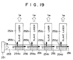
- Fig. 19 is a diagram of an array-type semiconductor integrated laser device according to a fifth embodiment of the present invention.
- the laser device shown in Fig. 19 comprises a master laser 251, slave lasers 252a - 252d, and light branching and amplifying devices 254a - 254d formed as shown in Fig. 15. Current is applied to each of the branching and amplifying devices 254a - 254d.
- the branching and amplifying device 254a receives a laser beam emitted from the master laser 251 via the waveguide 128 (Fig. 15).
- the laser beam emitted from the master laser 151 has a wavelength M .
- the branching and amplifying device 254a is allowed to pass through the laser beam to the waveguide 128 (Fig.
- the branching and amplifying devices 254a - 254b have the light amplifying function by injecting currents.
- the two laser beams emitted from the branching and amplifying device 254a respectively have a light intensity, for example, approximately equal to that of the laser beam from the master laser 251.
- the master laser 251 does not need to have a large driving ability determined taking into account loss which will occur if the branching and amplifying devices 254a - 254d are respectively formed with conventional reflectors.
- the laser beam propagated through the waveguide 130 is applied, as light 255a for synchronous oscillation, to the slave laser 252a. In response to the light 255a for synchronous oscillation, the slave laser 252a emits a laser beam having the wavelength ⁇ M .
- the laser beam propagated through the waveguide 128 coupled to the branching and amplifying device 254b is applied to the device 254b through its waveguide 128.
- the branching and amplifying device 254b emits light 255b for synchronous oscillation to the slave laser 252b and allows the light from the branching and amplifying device 254a to pass.
- the slave laser In response to the light 255b from the branching and amplifying device 254b, the slave laser emits a laser beam having the wavelength ⁇ M .
- the other slave lasers 252c and 252d respectively emit laser beams, each having the wavelength ⁇ M .
- reference number 256 indicates light directed to the master laser 251.
- the light 256 is prevented from being directed to each of the slave lasers 252a - 252d. If the light 256 is directed to the slave lasers 252a - 252d, the slave lasers 252a - 252d will not oscillate stably.
- each of the slave lasers 252a - 252d is prevented from passing through each of the branching and amplifying devices 254a - 254d or being reflected thereby. Since the branching and amplifying device according to the fifth embodiment of the present invention has the function shown in Fig. 14A, it is possible to stably oscillate the slave lasers 252a - 252d with the wavelength ⁇ M .
- the master laser 251 and the slave lasers 252a - 252d respectively have a buried double-hetero type stripe laser, which includes an undoped InGaAsP active layer having an oscillation wavelength 1.3 ⁇ m, n-type and p-type InP cladding layers provided on respective sides of the active layer, and a p + -type InGaAsP contact layer formed on the p-type InP layer.
- the master laser 251 and the slave lasers 252a - 252d can be formed by the photolithographic technique and the MOCVD process. Electrodes can be formed by a vacuum evaporation process.
- the master and slave lasers, and the branching and amplifying devices are integrally formed on the common n-type InP substrate 122 (Fig. 15).
- the master and slave lasers are coupled via the InGaAsP light guide layers 124 (Fig. 15).
- Each of the master and slave lasers separately has a p-type side electrode and an n-type side electrode.
- the slave lasers 252a - 252d have respective compositions of InGaAsP so that they have respective oscillation wavelengths slightly different from each other.
- the composition of InGaAsP of the light guide layer is selected so as to match the composition of the active layer of one of the slave lasers 252a - 252d which has the shortest wavelength.
- the pitches of the gratings of the branching and amplifying devices are made to match the wavelengths of the respective laser beams.
- the slave lasers 252a - 252d are modulated by external signals.
- the laser beams emitted from the slave lasers 252a - 252d are propagated through the InGaAsP light guide layer 124 in one direction and are then combined with each other, while the branching and amplifying devices 254a - 254d are biased in the forward direction so that they have suitable gains. There is no returning light, and hence the slave lasers 252a - 252d oscillate stably. Further, light is amplified by each of the branching and amplifying devices 254a - 254d. Hence, it is possible to transfer low intensity light.
Landscapes
- Physics & Mathematics (AREA)
- General Physics & Mathematics (AREA)
- Optics & Photonics (AREA)
- Condensed Matter Physics & Semiconductors (AREA)
- Electromagnetism (AREA)
- Engineering & Computer Science (AREA)
- Microelectronics & Electronic Packaging (AREA)
- Semiconductor Lasers (AREA)
- Optical Integrated Circuits (AREA)
Claims (21)
- Dispositif semi-conducteur optique comprenant :des première et seconde couches de revêtement (21, 27) etune structure de guide de lumière (22) intercalée entre les première et seconde couches de revêtement ;dans lequel la structure de guide de lumière a une structure de couche comprenant une première couche (22, 22a), une seconde couche (24, 24a) et une troisième couche (25, 25a), une pluralité de canaux étant formés périodiquement sur la surface de la première couche, la seconde couche (24) étant formée sur au moins des parties de ces canaux avec un indice de réfraction plus grand que celui de la première couche (22) et la troisième couche (25, 25a), ayant un indice de réfraction plus petit que celui de la seconde couche, étant formé sur la seconde couche, de sorte que la structure a une variation périodique d'indice de réfraction dans une direction prédéterminée, et une seconde variation périodique du gain optique de ladite direction prédéterminée, les première et seconde variations périodiques ayant des périodes identiques mais ayant une différence de phase pour que la structure montre un premier facteur de réflexion par rapport à la lumière entrante du côté gauche de celle-ci, et un second facteur de réflexion par rapport à la lumière ayant les mêmes propriétés que la lumière entrante par le côté gauche, mais entrant par le côté droit de celle-ci, les premier et second facteurs de réflexion étant différents l'un de l'autre.
- Dispositif semi-conducteur optique selon la revendication 1, dans lequel la première couche semi-conductrice (22) est une première partie de guide de lumière de la structure de couche de guide de lumière, la troisième couche semi-conductrice (25) a une fonction d'émission de lumière, et une structure de guide de lumière comprend une seconde partie de guide de lumière (26) formée sur la troisième couche semi-conductrice (25).
- Dispositif semi-conducteur optique selon la revendication 1 ou 2, dans lequel la première couche semi-conductrice (22a) est une première partie de guide de lumière de la structure de couche de guide de lumière et a une section en coupe transversale en dents de scie ; et la seconde couche semi-conductrice (24a) enterrant les canaux a une première épaisseur d'un côté de chaque canal et une seconde épaisseur, plus petite de l'autre côté.
- Dispositif semi-conducteur optique selon la revendication 1, dans lequel la seconde couche semi-conductrice (24b) est formée d'un côté de chaque canal de la première couche semi-conductrice (25d).
- Dispositif semi-conducteur optique selon la revendication 4, dans lequel la structure de couche de guide de lumière comprend une première partie de guide de lumière (22a) et une seconde partie de guide de lumière (26a), et la première couche semi-conductrice (25d) a une fonction d'émission de lumière et est formée sur la surface de ladite première partie (22a) de la structure de couche de guide de lumière, et la troisième couche semi-conductrice correspond à ladite seconde partie (26a) de la structure de couche de guide de lumière.
- Dispositif semi-conducteur optique selon l'une quelconque des revendications précédentes, comprenant en outre :
une première électrode (28) formée sur la première couche de revêtement ; et une seconde électrode (29) formée sur la seconde couche de revêtement. - Dispositif semi-conducteur optique selon l'une quelconque des revendications précédentes, dans lequel la différence de phase entre les première et seconde variations périodiques est comprise dans un intervalle prédéterminé autour de π/2 ou 3π/2.
- Dispositif semi-conducteur optique selon la revendication 3, dans lequel la seconde couche (134) a une surface incurvée périodiquement sur laquelle la troisième couche semi-conductrice (136) est formée.
- Dispositif semi-conducteur optique selon la revendication 2, dans lequel des canaux de la première couche semi-conductrice ont une coupe transversale approximativement rectangulaire.
- Appareil semi-conducteur optique comprenant un premier guide d'ondes (112) ; et un second guide d'ondes (114) coupant le premier guide d'ondes, dans lequel la partie d'intersection des premier et second guides d'ondes comprend un dispositif semi-conducteur optique selon l'une quelconque des revendications 1 à 9.
- Appareil semi-conducteur optique selon la revendication 10, dans lequel la structure de couche comprend un premier réseau (138) générant la variation d'indice de réfraction, et un second réseau (140) générant la variation de gain, les premier et second réseaux étant situés à un angle de π/4 par rapport à la direction de propagation de la lumière via le premier guide d'ondes.
- Appareil semi-conducteur optique selon la revendication 11, dans lequel le premier guide d'ondes croise le second guide d'ondes semi-conducteur à un angle φ et les premier et second réseaux sont obliquement disposés à un angle (π-φ)/2 par rapport à la direction de propagation de la lumière via le premier guide d'ondes.
- Dispositif semi-conducteur optique comprenant ; une fibre optique (41) et deux dispositifs semi-conducteur optiques selon l'une quelconque des revendications 1 à 9 reliés aux extrémités respectives de la fibre optique.
- Dispositif laser semi-conducteur comprenant deux dispositifs semi-conducteur optiques selon l'une quelconque des revendications 1 à 9, et des fibres optiques (53, 54) reliées aux deux dispositifs semi-conducteurs optiques pour qu'un dispositif laser en forme d'anneau soit formé.
- Dispositif laser semi-conducteur comprenant un réseau de laser semi-conducteur (252) formé sur un substrat ; et des dispositifs semi-conducteur optiques (254) selon l'une quelconque des revendications 1 à 9, agissant comme dispositifs de dérivation et d'amplification de lumière et couplant les lasers semi-conducteurs afin de former le réseau.
- Dispositif laser semi-conducteur selon la revendication 15, comprenant en outre un laser maître (251) formé sur le substrat et couplé à un (254a) des dispositifs de dérivation et d'amplification de lumière.
- Dispositif laser semi-conducteur selon la revendication 5, dans lequel la différence de phase entre les première et seconde variations périodiques est compris dans un intervalle prédéterminé autour de π/2 ou 3π/2.
- Dispositif laser semi-conducteur selon la revendication 15, dans lequel les premier et second réseaux sont situés à un angle égal à π/4 par rapport à la direction de propagation de lumière.
- Procédé de fabrication d'un dispositif semi-conducteur optique selon l'une quelconque des revendications 1 à 9 comprenant les étapes de :(a) formation de la première couche sur une base, la première couche servant comme une couche de guide de lumière, et d'une couche active ;(b) formation d'une pluralité de canaux sur la surface de la première couche ;(c) projection obliquement d'un gaz sur la surface de la première couche pour que la seconde couche ayant un indice de réfraction plus grand que celui de la première couche soit formé sur au moins des parties des canaux ; et(d) formation d'une troisième couche sur la seconde couche, la troisième couche ayant un indice de réfraction plus petit que celui de la seconde couche servant soit comme couche active soit comme couche de guide de lumière.
- Procédé selon la revendication 19, dans lequel l'étape (b) comprend l'étape de formation de motif sur la surface de la première couche pour que les canaux aient chacun une coupe transversale approximativement rectangulaire donnée.
- Procédé selon la revendication 19, dans lequel l'étape (b) comprend l'étape de formation de motif sur la surface de la première couche pour que les canaux aient chacun une coupe transversale en dents de scie donnée.
Applications Claiming Priority (6)
| Application Number | Priority Date | Filing Date | Title |
|---|---|---|---|
| JP23614491A JPH0575211A (ja) | 1991-09-17 | 1991-09-17 | 光半導体装置およびそれを用いたレーザ装置 |
| JP236144/91 | 1991-09-17 | ||
| JP30818391A JPH05145191A (ja) | 1991-11-25 | 1991-11-25 | 半導体装置及びその製造方法 |
| JP308183/91 | 1991-11-25 | ||
| JP177123/92 | 1992-07-03 | ||
| JP17712392A JPH0621580A (ja) | 1992-07-03 | 1992-07-03 | 集積化光半導体装置 |
Publications (3)
| Publication Number | Publication Date |
|---|---|
| EP0533475A2 EP0533475A2 (fr) | 1993-03-24 |
| EP0533475A3 EP0533475A3 (en) | 1993-09-01 |
| EP0533475B1 true EP0533475B1 (fr) | 1997-07-02 |
Family
ID=27324369
Family Applications (1)
| Application Number | Title | Priority Date | Filing Date |
|---|---|---|---|
| EP92308484A Expired - Lifetime EP0533475B1 (fr) | 1991-09-17 | 1992-09-17 | Dispositif semi-conducteur optique, méthode de production et dispositif laser utilisant des dispositifs semi-conducteur optiques |
Country Status (3)
| Country | Link |
|---|---|
| US (1) | US5347533A (fr) |
| EP (1) | EP0533475B1 (fr) |
| DE (1) | DE69220636T2 (fr) |
Families Citing this family (17)
| Publication number | Priority date | Publication date | Assignee | Title |
|---|---|---|---|---|
| US5500916A (en) * | 1994-09-09 | 1996-03-19 | At&T Corp. | Method for making Bragg reflectors for waveguides |
| US5657407A (en) * | 1995-06-07 | 1997-08-12 | Biota Corp. | Optical waveguide coupling device having a parallelogramic grating profile |
| US5727013A (en) * | 1995-10-27 | 1998-03-10 | Wisconsin Alumni Research Foundation | Single lobe surface emitting complex coupled distributed feedback semiconductor laser |
| AUPN694795A0 (en) * | 1995-12-01 | 1996-01-04 | University Of Sydney, The | Distributed feedback ring laser |
| JP3714430B2 (ja) * | 1996-04-15 | 2005-11-09 | シャープ株式会社 | 分布帰還型半導体レーザ装置 |
| US5926493A (en) * | 1997-05-20 | 1999-07-20 | Sdl, Inc. | Optical semiconductor device with diffraction grating structure |
| JP4375834B2 (ja) * | 1998-03-19 | 2009-12-02 | シャープ株式会社 | 利得結合型分布帰還半導体レーザ装置及びその製造方法 |
| US6285698B1 (en) * | 1998-09-25 | 2001-09-04 | Xerox Corporation | MOCVD growth of InGaN quantum well laser structures on a grooved lower waveguiding layer |
| AU6628700A (en) | 1999-08-13 | 2001-03-13 | Wisconsin Alumni Research Foundation | Single mode, single lobe surface emitting distributed feedback semiconductor laser |
| US7457340B2 (en) * | 2002-01-18 | 2008-11-25 | Wisconsin Alumni Research Foundation | High coherent power, two-dimensional surface-emitting semiconductor diode array laser |
| AU2003207591A1 (en) * | 2002-01-18 | 2003-09-02 | Wisconsin Alumini Research Foundation | High coherent power, two-dimensional surfaceemitting semiconductor diode array laser |
| JP2004088049A (ja) * | 2002-03-08 | 2004-03-18 | Mitsubishi Electric Corp | 光半導体装置 |
| KR100584412B1 (ko) * | 2003-10-10 | 2006-05-26 | 삼성전자주식회사 | 이득 고정된 반도체 광증폭기 |
| US7403552B2 (en) * | 2006-03-10 | 2008-07-22 | Wisconsin Alumni Research Foundation | High efficiency intersubband semiconductor lasers |
| US7457338B2 (en) * | 2006-04-19 | 2008-11-25 | Wisconsin Alumni Research Foundation | Quantum well lasers with strained quantum wells and dilute nitride barriers |
| US7408966B2 (en) * | 2006-08-18 | 2008-08-05 | Wisconsin Alumni Research Foundation | Intersubband quantum box stack lasers |
| CN115632244A (zh) * | 2022-10-11 | 2023-01-20 | 北京爱杰光电科技有限公司 | 天线结构 |
Family Cites Families (13)
| Publication number | Priority date | Publication date | Assignee | Title |
|---|---|---|---|---|
| US4178604A (en) * | 1973-10-05 | 1979-12-11 | Hitachi, Ltd. | Semiconductor laser device |
| US4728168A (en) * | 1984-01-20 | 1988-03-01 | American Telephone And Telegraph Company, At&T Bell Laboratories | Composite cavity laser utilizing an intra-cavity electrooptic waveguide device |
| JPS61222189A (ja) * | 1985-03-15 | 1986-10-02 | Sharp Corp | 半導体レ−ザ |
| JPS6289383A (ja) * | 1985-10-16 | 1987-04-23 | Matsushita Electric Ind Co Ltd | 半導体レ−ザ |
| JPS63293892A (ja) * | 1987-05-27 | 1988-11-30 | Hitachi Ltd | 半導体レ−ザ装置 |
| JPH01248585A (ja) * | 1988-03-30 | 1989-10-04 | Kokusai Denshin Denwa Co Ltd <Kdd> | 分布帰還形半導体レーザ |
| JPH0232582A (ja) * | 1988-07-22 | 1990-02-02 | Oki Electric Ind Co Ltd | 集積型半導体レーザとその製造方法 |
| JP2733263B2 (ja) * | 1988-10-04 | 1998-03-30 | キヤノン株式会社 | 集積型光ノードおよびそれを用いたバス型光情報システム |
| US4942366A (en) * | 1989-03-21 | 1990-07-17 | General Electric Company | Amplifier device with coupled surface emitting grating |
| DE69027368T2 (de) * | 1989-06-30 | 1997-01-30 | Optical Measurement Technology | Halbleiterlaser und Verfahren zur Herstellung desselben |
| JPH0358410A (ja) * | 1989-07-26 | 1991-03-13 | Nec Corp | 半導体構造の製造方法 |
| JPH0384924A (ja) * | 1989-08-29 | 1991-04-10 | Matsushita Electric Ind Co Ltd | 半導体装置の製造方法 |
| US5050949A (en) * | 1990-06-22 | 1991-09-24 | At&T Bell Laboratories | Multi-stage optical fiber amplifier |
-
1992
- 1992-09-15 US US07/945,484 patent/US5347533A/en not_active Expired - Lifetime
- 1992-09-17 EP EP92308484A patent/EP0533475B1/fr not_active Expired - Lifetime
- 1992-09-17 DE DE69220636T patent/DE69220636T2/de not_active Expired - Fee Related
Non-Patent Citations (1)
| Title |
|---|
| 831 - 833 J. WILLEMS ET AL 'Filter characteristics of DBR amplifier with index and gain coupling.' * |
Also Published As
| Publication number | Publication date |
|---|---|
| EP0533475A3 (en) | 1993-09-01 |
| EP0533475A2 (fr) | 1993-03-24 |
| DE69220636T2 (de) | 1997-10-16 |
| DE69220636D1 (de) | 1997-08-07 |
| US5347533A (en) | 1994-09-13 |
Similar Documents
| Publication | Publication Date | Title |
|---|---|---|
| EP0533475B1 (fr) | Dispositif semi-conducteur optique, méthode de production et dispositif laser utilisant des dispositifs semi-conducteur optiques | |
| US5349602A (en) | Broad-area MOPA device with leaky waveguide beam expander | |
| US6483863B2 (en) | Asymmetric waveguide electroabsorption-modulated laser | |
| US6917729B2 (en) | Tailored index single mode optical amplifiers and devices and systems including same | |
| US5710847A (en) | Semiconductor optical functional device | |
| CN104937791B (zh) | 激光装置、光调制装置以及光半导体元件 | |
| EP1052747B1 (fr) | Laser semi-conducteur à mode unique | |
| KR100701006B1 (ko) | 포물선 도파로형 평행광 렌즈 및 이를 포함한 파장 가변외부 공진 레이저 다이오드 | |
| US5282080A (en) | Surface coupled optical amplifier | |
| EP0735635B1 (fr) | Appareil optique semi-conducteur, sa méthode de commande, appareil source lumineuse et système de communication optique utilisant celui-ci | |
| US5220573A (en) | Optical apparatus using wavelength selective photocoupler | |
| US5444730A (en) | Single-wavelength semiconductor laser | |
| US20040105476A1 (en) | Planar waveguide surface emitting laser and photonic integrated circuit | |
| US6445722B2 (en) | Single-transverse-mode laser diode with multi-mode waveguide region and manufacturing method of the same | |
| US5838854A (en) | Integrated optical control element and a method for fabricating the same and optical integrated circuit element and optical integrated circuit device using the same | |
| JP2624279B2 (ja) | スラブ導波光出射半導体レーザー | |
| US6205163B1 (en) | Single-transverse-mode 1×N multi-mode interferometer type semiconductor laser device | |
| JP2001500280A (ja) | 導波体の相互結合のための装置 | |
| JP2947142B2 (ja) | 波長可変半導体レーザ | |
| JPS63111689A (ja) | 分布帰還型半導体レ−ザ | |
| US20030103761A1 (en) | Folded light path for planar optical devices | |
| JPH09307179A (ja) | 位相シフト型分布帰還半導体レーザ | |
| JPS63299291A (ja) | 半導体レ−ザ | |
| JPH084179B2 (ja) | 半導体レ−ザ | |
| JPH09289357A (ja) | 光半導体装置、その製造方法、駆動方法、及びこれらを使ったシステム |
Legal Events
| Date | Code | Title | Description |
|---|---|---|---|
| PUAI | Public reference made under article 153(3) epc to a published international application that has entered the european phase |
Free format text: ORIGINAL CODE: 0009012 |
|
| AK | Designated contracting states |
Kind code of ref document: A2 Designated state(s): DE FR GB |
|
| PUAL | Search report despatched |
Free format text: ORIGINAL CODE: 0009013 |
|
| AK | Designated contracting states |
Kind code of ref document: A3 Designated state(s): DE FR GB |
|
| 17P | Request for examination filed |
Effective date: 19940223 |
|
| 17Q | First examination report despatched |
Effective date: 19950524 |
|
| GRAG | Despatch of communication of intention to grant |
Free format text: ORIGINAL CODE: EPIDOS AGRA |
|
| GRAH | Despatch of communication of intention to grant a patent |
Free format text: ORIGINAL CODE: EPIDOS IGRA |
|
| GRAH | Despatch of communication of intention to grant a patent |
Free format text: ORIGINAL CODE: EPIDOS IGRA |
|
| GRAA | (expected) grant |
Free format text: ORIGINAL CODE: 0009210 |
|
| AK | Designated contracting states |
Kind code of ref document: B1 Designated state(s): DE FR GB |
|
| REF | Corresponds to: |
Ref document number: 69220636 Country of ref document: DE Date of ref document: 19970807 |
|
| ET | Fr: translation filed | ||
| PLBE | No opposition filed within time limit |
Free format text: ORIGINAL CODE: 0009261 |
|
| 26N | No opposition filed | ||
| REG | Reference to a national code |
Ref country code: GB Ref legal event code: IF02 |
|
| PGFP | Annual fee paid to national office [announced via postgrant information from national office to epo] |
Ref country code: FR Payment date: 20050823 Year of fee payment: 14 |
|
| PGFP | Annual fee paid to national office [announced via postgrant information from national office to epo] |
Ref country code: GB Payment date: 20050914 Year of fee payment: 14 |
|
| PGFP | Annual fee paid to national office [announced via postgrant information from national office to epo] |
Ref country code: DE Payment date: 20050915 Year of fee payment: 14 |
|
| PG25 | Lapsed in a contracting state [announced via postgrant information from national office to epo] |
Ref country code: DE Free format text: LAPSE BECAUSE OF NON-PAYMENT OF DUE FEES Effective date: 20070403 |
|
| GBPC | Gb: european patent ceased through non-payment of renewal fee |
Effective date: 20060917 |
|
| REG | Reference to a national code |
Ref country code: FR Ref legal event code: ST Effective date: 20070531 |
|
| PG25 | Lapsed in a contracting state [announced via postgrant information from national office to epo] |
Ref country code: GB Free format text: LAPSE BECAUSE OF NON-PAYMENT OF DUE FEES Effective date: 20060917 |
|
| PG25 | Lapsed in a contracting state [announced via postgrant information from national office to epo] |
Ref country code: FR Free format text: LAPSE BECAUSE OF NON-PAYMENT OF DUE FEES Effective date: 20061002 |