EP0229509A2 - Revêtement transparent, stable, à grande résistance - Google Patents
Revêtement transparent, stable, à grande résistance Download PDFInfo
- Publication number
- EP0229509A2 EP0229509A2 EP86309839A EP86309839A EP0229509A2 EP 0229509 A2 EP0229509 A2 EP 0229509A2 EP 86309839 A EP86309839 A EP 86309839A EP 86309839 A EP86309839 A EP 86309839A EP 0229509 A2 EP0229509 A2 EP 0229509A2
- Authority
- EP
- European Patent Office
- Prior art keywords
- oxide
- electrical resistance
- doped
- undoped
- metal
- Prior art date
- Legal status (The legal status is an assumption and is not a legal conclusion. Google has not performed a legal analysis and makes no representation as to the accuracy of the status listed.)
- Withdrawn
Links
Images



Classifications
-
- G—PHYSICS
- G03—PHOTOGRAPHY; CINEMATOGRAPHY; ANALOGOUS TECHNIQUES USING WAVES OTHER THAN OPTICAL WAVES; ELECTROGRAPHY; HOLOGRAPHY
- G03G—ELECTROGRAPHY; ELECTROPHOTOGRAPHY; MAGNETOGRAPHY
- G03G5/00—Recording-members for original recording by exposure, e.g. to light, to heat or to electrons; Manufacture thereof; Selection of materials therefor
- G03G5/02—Charge-receiving layers
- G03G5/04—Photoconductive layers; Charge-generation layers or charge-transporting layers; Additives therefor; Binders therefor
- G03G5/08—Photoconductive layers; Charge-generation layers or charge-transporting layers; Additives therefor; Binders therefor characterised by the photoconductive material being inorganic
- G03G5/082—Photoconductive layers; Charge-generation layers or charge-transporting layers; Additives therefor; Binders therefor characterised by the photoconductive material being inorganic and not being incorporated in a bonding material, e.g. vacuum deposited
-
- G—PHYSICS
- G03—PHOTOGRAPHY; CINEMATOGRAPHY; ANALOGOUS TECHNIQUES USING WAVES OTHER THAN OPTICAL WAVES; ELECTROGRAPHY; HOLOGRAPHY
- G03G—ELECTROGRAPHY; ELECTROPHOTOGRAPHY; MAGNETOGRAPHY
- G03G5/00—Recording-members for original recording by exposure, e.g. to light, to heat or to electrons; Manufacture thereof; Selection of materials therefor
- G03G5/02—Charge-receiving layers
- G03G5/0202—Dielectric layers for electrography
Definitions
- the present invention relates to high resistance transparent coatings, and specifically methods for formulating such coatings so as to increase an electrical resistance thereof, and useful articles including such increased resistance coatings.
- High resistance transparent coatings have numerous applications. For example, when copying images using electrostatic imaging, it is common to subject a film having a dielectric material on a surface thereof to an electrical potential so as to selectively dispose electrostatic charge thereon which is then developed by applying a toner onto the surface of the film.
- the film itself comprises the dielectric material layered over a high resistance transparent coating which is laid over a substrate, such as polyester.
- the high resistance transparent coating functions as a ground plane and is therefore required to have an electrical resistance within a predetermined range such that the coating can function as required.
- the ground plane coating is unduly conductive which results in ghost images being formed by electrodes in close proximity to other electrodes which create an electrical potential for depositing an electric charge on the dielectric.
- the electrical resistance of the ground plane coating is unduly large, the time constant for deposition of charge on the film becomes too long resulting in very slow image formation, typical excessively high resistances being those above 20 mega ohms per square.
- the present invention seeks to eliminate the above- noted drawbacks, and to provide an improved coating which is highly stable and which also can be formulated so to have any one of many desired electrical resistances and good optical transparency, especially at visible light wavelengths, so as to be suitable as a ground plane coating for electrostatic imaging processes.
- a coating which comprises a partially transparent conductive coating which includes a wide band gap semiconducting oxide which is doped with an appropriate material so as to vary the electrical resistance of the oxide significantly from that otherwise obtainable from an undoped identical oxide.
- the invention provides a method of forming a partially transparent conductive coating, comprising the steps of:
- the invention provides an apparatus for storing information by supporting electrostatic charges, comprising:
- the invention also provides a high resistance partially transparent conductive coating, comprising a wide band gap semiconducting oxide, an undoped composition thereof having a first electrical resistance, the oxide being doped so as to form a doped wide band gap semiconducting oxide whose electrical resistance is increased by an amount greater than an order of magnitude over the undoped composition, the doped oxide being of a type whose electrical resistance first reaches an interim maximum and then reaches an interim minimum as its oxygen concentration is increased, an oxygen concentration of the doped oxide being within + 5% of an oxygen concentration yielding the interim minimum electrical resistance.
- the invention provides a method of forming a ground plane for an apparatus for storing information by supporting electrostatic charges on a dielectric layer disposed on the ground plane, comprising the steps of:
- a film containing a wide band gap semiconducting coating is formed as a ground plane for electrostatic recording.
- a preferred embodiment is to utilize tin oxide.
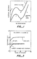
- Figure 1 illustrates a typical graph for a coating of tin oxide showing how its electrical resistance varies as a function of an oxygen concentration of the tin oxide.
- the electrical resistance of an undoped tin oxide coating initially goes up with its oxygen concentration, until it reaches a peak identified by reference numeral 1, and thereafter the electrical resistance of the undoped coating goes down with a further increase in the oxygen concentration until it reaches a minimum value at reference numeral 2, and thereafter the electrical resistance of the coating rises with further increases in the oxygen concentration. Only coatings with oxygen concentrations greater than about that of the coating 1 are highly transparent.
- the operating point 2 results in an electrical resistance of about 2 kohm per square for coatings about 500 angstroms thick, this particular electrical resistance is not optimum for the end use of the coating desired.
- an operating point such as that identified by reference numeral 3 may achieve a predetermined electrical resistance 4, the electrical resistance 4 of the undoped tin oxide coating at this point is highly unstable. Specifically, if during manufacture a small variation in the oxygen concentration occurs, a magnified change in the resistance occurs. Furthermore, in use, oxygen migration within the coating further changes the electrical resistance. Therefore, product reliability is relatively low.
- a coating from the undoped tin oxide material may be manufactured with a higher resistance by making the coating thinner, but this method cannot increase the resistance by a factor of more than about 5 as thin coatings, especially coatings thinner than 100 angstroms, are mechanically and environmentally unstable.
- the tin oxide is doped during its formation with a metal, for example copper or aluminum, by a specified amount so as to increase an electrical resistivity of the tin oxide in amounts sufficient such that its intermediate minimum electrical resistance point 6 results in the coating having the desired electrical resistance 4.
- the coating not only has the optimum electrical resistance, it furthermore has optimum stability since small changes in the oxygen concentration of the coating which result either during its manufacture or subsequent thereto due to environmental conditions which may induce chemical alterations of the coating result in minimum changes of the electrical resistance of the coating.
- the oxygen concen- tation chosen is optimized such that the electrical resistance of the doped coating corresponds to the intermediate minimum electrical resistance for the doped coating.
- the actual oxygen concentration used can be + 2% different from the optimum concentration, and even + 5% different, though as the difference gets larger, the stability worsens.
- a tin oxide coating doped with aluminum and which has a resistivity of 1 mega ohm per square at operating point 6 may have a higher visible light transmittance than a tin oxide coating doped with copper to have a resistivity of 1 mega ohm per square at operating point 6.
- other consideratons could lead one to chose a dopant with decreased visible light transmittance, such as ease of manufacture.
- copper does slightly reduce the doped coating visible light transmittance
- copper has other advantages over aluminum for doping tin oxide such as ease of sputtering.
- tin oxide is referred to as one preferred embodiment for which the invention is suitable
- other oxides can also be used within the scope of the invention, and in particular any oxide which comprises a wide band gap semiconducting oxide.
- Suitable metals for forming such oxides include indium, zinc, cadmium and lead for example.
- the metal chosen to dope the oxide so as to increase its electrical resistivity in amounts sufficient such that the operating point 6 is optimally stable is any metal which has an odd number of electrons more or less than the which forms a semiconducting oxide.
- Other elements with different electronic shell configurations may also be chosen.
- a series of coatings was made on PET polyester film by reactive sputter deposition of composite tin/copper targets in atmospheres containing various partial pressures of oxygen gas.
- the ratio of tin to copper was varied systematically, as was the partial pressure of oxygen in the reactive sputtering discharge, to obtain a series of coatings with different tin, copper, and oxygen concentrations. The properties of these coatings were then measured and the coatings were then subjected to accelerated aging to determine their environmental stabilities.
- Composite tin/copper sputtering targets were fabricated by placing pie-shaped copper segments on a 10 cm diameter tin disc. Targets were fabricated with 4, 8, 14 and 17% surface coverage by copper, respectively. For each composition, a series of coatings was made at various oxygen partial pressures.
- the coating conditions were as follows:
- the oxygen partial pressure range varied for each target composition, but by way of example, a range of 1.3 to 1.8 mTorr was used to sputter the target with 14% copper coverage of the tin. A thickness of the coatings produced was maintained relatively constant at about 400 angstroms. A graph of the electrical resistances of the coatings and of their visible light transmittances as a function of oxygen partial pressure is illustrated in Figure 2 for the 14% copper percent coverage. The coating produced with an oxygen partial pressure of 1.5 mTorr was found to have the lowest stable electrical resistance of these coatings. Figure 3 shows that this coating exhibits remarkable environmental stability in air, 100°C dry heat, and 60°C 95% relative humidity.
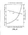
- Figure 4 shows the electrical resistance and visible light transmission of the most stable coating produced with each composite target.
- this most stable coating was found to be that with the minimum electrical resistance, e.g., an oxygen concentration at or close to the operating point 6 in Figure 1.
- the curve of Figure 4 allows one to predict the surface target coverage which will be necessary to produce a stable transparent coating with a desired electrical resistance.
- the invention is capable of yielding coatings having minimum most stable electrical resistances orders of magnitude greater than similarly constructed undoped coatings, Figures 2 and 4 showing increases of at least 1, 2, 3, 4, 5, and 6 orders of magnitude and more.
- Example 2 A second series of experiments was performed using the same apparatus and general procedures used in Example 1, with the exception that the composite sputtering target was made by placing pie-shaped segments of aluminum, rather than copper, on a tin target. Targets were fabricated with 23, 35, 42, 50, 60, and 70% aluminum coverage, respectively.
- the coating conditions were as follows:
- the oxygen partial pressure was varied for each target composition.
- the oxygen partial pressure was varied from 0.7 to 1.25 mTorr for a 60% aluminum on tin target.
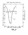
- Figure 5 shows the behavior of the electrical resistance and the visible light transmittance as a function of oxygen partial pressure for 60% aluminum target coverage.
- the coating was most stable and its environmental stability is demonstrated by the data presented in Figure 6.
- This procedure was repeated for each of the tin-aluminum target coverage conditions given above, and the data presented in Figure 7 shows the electrical resistance and visible light transmittance of the most stable coating produced at each target coverage level. In all cases, the most stable coating was found to be that with the minimum electrical resistance. This curve allows the target coverage level to be predicted which will produce a stable transparent coating with a desired electrical resistance.
- Examples 1 and 2 and Figures 2-7 indicate, once a particular electrical resistance of a wide band gap semiconducting oxide is chosen, the examples all being directed to tin oxide, in accordance with the teachings of the present invention suitable metal dopants can be added to the oxide in its formation so as to precisely control the operating point 6 and its electrical resistance so that the electrical resistance at the operating point 6 of Figure 1 can be made to correspond with the desired electrical resistance whereat the coating is most stable.
- Preferred embodiments of the invention include coatings having a thickness between 100-2000 angstroms, more preferably between 200-1000 angstroms, and most preferably between 300-600 angstroms.
- a preferred use of the invention is for the production of a film to be used for electrostatic imaging, as illustrated in Figure 8 whereat the film 10 includes a dielectric layer 11 disposed over a partially transparent high resistance coating 12 made in accordance with the present invention, which is disposed over a substrate 13, such as plastic.
- the coating 12 must have an electrical resistance which is sufficiently high such that its electrical conductivity in the direction of arrows 12 is not so large so as to conduct current to electrode 15 remote from an electrode 16 used to generate an electric field to deposit a charge 18 on a surface of the dielectric layer 11.
- an electrical resistance of the coating 12 must be relatively high.
- the coating 12 must have an electrical resistance which is not too large and also which is not too low.
- optimum values of the electrical resistance of the coating 12 can be determined, and subsequently utilizing the teachings of the present invention of doping the coating 12 as it is formulated, it is a straightforward procedure to produce a coating 12 having a desired thickness and the desired electrical resistance which also corresponds to a minimum electrical resistance within a range of oxygen concentrations of the particular oxide being used.
Landscapes
- Physics & Mathematics (AREA)
- General Physics & Mathematics (AREA)
- Chemical & Material Sciences (AREA)
- Inorganic Chemistry (AREA)
- Non-Insulated Conductors (AREA)
- Paints Or Removers (AREA)
- Conductive Materials (AREA)
- Thermistors And Varistors (AREA)
- Photoreceptors In Electrophotography (AREA)
- Apparatuses And Processes For Manufacturing Resistors (AREA)
- Non-Adjustable Resistors (AREA)
- Manufacturing Of Electric Cables (AREA)
Applications Claiming Priority (2)
| Application Number | Priority Date | Filing Date | Title |
|---|---|---|---|
| US06/811,126 US4710441A (en) | 1985-12-18 | 1985-12-18 | Stable high resistance transparent coating |
| US811126 | 1985-12-18 |
Publications (2)
| Publication Number | Publication Date |
|---|---|
| EP0229509A2 true EP0229509A2 (fr) | 1987-07-22 |
| EP0229509A3 EP0229509A3 (fr) | 1989-11-29 |
Family
ID=25205641
Family Applications (1)
| Application Number | Title | Priority Date | Filing Date |
|---|---|---|---|
| EP86309839A Withdrawn EP0229509A3 (fr) | 1985-12-18 | 1986-12-17 | Revêtement transparent, stable, à grande résistance |
Country Status (4)
| Country | Link |
|---|---|
| US (1) | US4710441A (fr) |
| EP (1) | EP0229509A3 (fr) |
| JP (1) | JPS62177902A (fr) |
| CA (1) | CA1322736C (fr) |
Families Citing this family (6)
| Publication number | Priority date | Publication date | Assignee | Title |
|---|---|---|---|---|
| US4814036A (en) * | 1985-07-17 | 1989-03-21 | Velcro Industries B.V. | Method for adapting separable fasteners for attachment to other objects |
| US5714248A (en) * | 1996-08-12 | 1998-02-03 | Xerox Corporation | Electrostatic imaging member for contact charging and imaging processes thereof |
| US6248490B1 (en) * | 1998-12-01 | 2001-06-19 | Canon Kabushiki Kaisha | Electrophotographic photosensitive member, process cartridge, and electrophotographic apparatus |
| US7867625B2 (en) * | 2002-06-13 | 2011-01-11 | Nihon New Chrome Co., Ltd. | Copper-tin-oxygen alloy plating |
| AU2003244119A1 (en) * | 2002-06-13 | 2003-12-31 | Nihon New Chrome Co., Ltd. | Copper-tin-oxygen based alloy plating |
| JP2015108730A (ja) * | 2013-12-05 | 2015-06-11 | 株式会社リコー | 電子写真感光体、画像形成装置、及びプロセスカートリッジ |
Family Cites Families (5)
| Publication number | Priority date | Publication date | Assignee | Title |
|---|---|---|---|---|
| DE2926856A1 (de) * | 1978-07-04 | 1980-01-17 | Kanzaki Paper Mfg Co Ltd | Elektrostatisches aufzeichnungsmaterial |
| US4246143A (en) * | 1978-07-12 | 1981-01-20 | Matsushita Electric Industrial Co., Ltd. | Process of preparing conductive tin dioxide powder |
| JPS56138742A (en) * | 1980-03-31 | 1981-10-29 | Konishiroku Photo Ind Co Ltd | Charge retaining material and method for forming copy image using this material |
| US4515882A (en) * | 1984-01-03 | 1985-05-07 | Xerox Corporation | Overcoated electrophotographic imaging system |
| JPH0731950B2 (ja) * | 1985-11-22 | 1995-04-10 | 株式会社リコー | 透明導電膜の製造方法 |
-
1985
- 1985-12-18 US US06/811,126 patent/US4710441A/en not_active Expired - Fee Related
-
1986
- 1986-12-16 CA CA000525467A patent/CA1322736C/fr not_active Expired - Fee Related
- 1986-12-17 EP EP86309839A patent/EP0229509A3/fr not_active Withdrawn
- 1986-12-18 JP JP61302720A patent/JPS62177902A/ja active Pending
Also Published As
| Publication number | Publication date |
|---|---|
| CA1322736C (fr) | 1993-10-05 |
| US4710441A (en) | 1987-12-01 |
| EP0229509A3 (fr) | 1989-11-29 |
| JPS62177902A (ja) | 1987-08-04 |
Similar Documents
| Publication | Publication Date | Title |
|---|---|---|
| US4020389A (en) | Electrode construction for flexible electroluminescent lamp | |
| US5045235A (en) | Transparent conductive film | |
| US3655545A (en) | Post heating of sputtered metal oxide films | |
| EP0204554A2 (fr) | Dispositif photoconducteur comportant une couche conductrice transparente d'oxyde de zinc | |
| US4959257A (en) | Transparencies | |
| US5289155A (en) | Positive temperature characteristic thermistor and manufacturing method therefor | |
| KR100345759B1 (ko) | 흡광성무반사처리필름을갖춘유기기판및이의제조방법 | |
| US4605565A (en) | Method of depositing a highly conductive, highly transmissive film | |
| US4710441A (en) | Stable high resistance transparent coating | |
| US3749658A (en) | Method of fabricating transparent conductors | |
| US4675092A (en) | Method of producing thin film electroluminescent structures | |
| US3258413A (en) | Method for the fabrication of tantalum film resistors | |
| US4069356A (en) | Method for rapidly forming photoconductive layers for integrated circuits | |
| JPH04272612A (ja) | 透明電極 | |
| JP3507623B2 (ja) | 透明導電膜の製造方法及びそれを用いた薄膜太陽電池 | |
| US4948529A (en) | Stable high resistance transparent coating | |
| US3139396A (en) | Tin oxide resistors | |
| JP2989886B2 (ja) | アナログ式タツチパネル | |
| JPH0945140A (ja) | 酸化亜鉛系透明導電性膜 | |
| US3388053A (en) | Method of preparing a film resistor by sputtering a ternary alloy of tin, antimony and indium in the presence of oxygen | |
| Ridge et al. | Composition control in conducting oxide thin films | |
| US3027277A (en) | Method of producing transparent electrically conductive coatings and coated article | |
| US3832298A (en) | Method for producing a photoconductive element | |
| US3114045A (en) | Photo-conductive translucent electroluminescent device and method of manufacture | |
| US3803057A (en) | Resistive materials and method of making such materials |
Legal Events
| Date | Code | Title | Description |
|---|---|---|---|
| PUAI | Public reference made under article 153(3) epc to a published international application that has entered the european phase |
Free format text: ORIGINAL CODE: 0009012 |
|
| 17P | Request for examination filed |
Effective date: 19861224 |
|
| AK | Designated contracting states |
Kind code of ref document: A2 Designated state(s): AT BE CH DE ES FR GB GR IT LI NL SE |
|
| PUAL | Search report despatched |
Free format text: ORIGINAL CODE: 0009013 |
|
| AK | Designated contracting states |
Kind code of ref document: A3 Designated state(s): AT BE CH DE ES FR GB GR IT LI NL SE |
|
| 17Q | First examination report despatched |
Effective date: 19911113 |
|
| RAP1 | Party data changed (applicant data changed or rights of an application transferred) |
Owner name: COURTAULDS PERFORMANCE FILMS, INC. |
|
| STAA | Information on the status of an ep patent application or granted ep patent |
Free format text: STATUS: THE APPLICATION IS DEEMED TO BE WITHDRAWN |
|
| 18D | Application deemed to be withdrawn |
Effective date: 19940107 |
|
| RIN1 | Information on inventor provided before grant (corrected) |
Inventor name: KITTLER, WILFRED, C. Inventor name: RITCHIE, IAN THOMAS |