EP0230241A1 - Système indicateur multiple - Google Patents
Système indicateur multiple Download PDFInfo
- Publication number
- EP0230241A1 EP0230241A1 EP87100262A EP87100262A EP0230241A1 EP 0230241 A1 EP0230241 A1 EP 0230241A1 EP 87100262 A EP87100262 A EP 87100262A EP 87100262 A EP87100262 A EP 87100262A EP 0230241 A1 EP0230241 A1 EP 0230241A1
- Authority
- EP
- European Patent Office
- Prior art keywords
- decoding means
- data
- identification number
- decoder
- display
- Prior art date
- Legal status (The legal status is an assumption and is not a legal conclusion. Google has not performed a legal analysis and makes no representation as to the accuracy of the status listed.)
- Granted
Links
Images




Classifications
-
- H—ELECTRICITY
- H04—ELECTRIC COMMUNICATION TECHNIQUE
- H04N—PICTORIAL COMMUNICATION, e.g. TELEVISION
- H04N5/00—Details of television systems
- H04N5/44—Receiver circuitry for the reception of television signals according to analogue transmission standards
- H04N5/445—Receiver circuitry for the reception of television signals according to analogue transmission standards for displaying additional information
-
- H—ELECTRICITY
- H04—ELECTRIC COMMUNICATION TECHNIQUE
- H04M—TELEPHONIC COMMUNICATION
- H04M11/00—Telephonic communication systems specially adapted for combination with other electrical systems
- H04M11/08—Telephonic communication systems specially adapted for combination with other electrical systems specially adapted for optional reception of entertainment or informative matter
- H04M11/085—Telephonic communication systems specially adapted for combination with other electrical systems specially adapted for optional reception of entertainment or informative matter using a television receiver, e.g. viewdata system
-
- G—PHYSICS
- G06—COMPUTING OR CALCULATING; COUNTING
- G06F—ELECTRIC DIGITAL DATA PROCESSING
- G06F3/00—Input arrangements for transferring data to be processed into a form capable of being handled by the computer; Output arrangements for transferring data from processing unit to output unit, e.g. interface arrangements
- G06F3/14—Digital output to display device ; Cooperation and interconnection of the display device with other functional units
- G06F3/153—Digital output to display device ; Cooperation and interconnection of the display device with other functional units using cathode-ray tubes
-
- G—PHYSICS
- G09—EDUCATION; CRYPTOGRAPHY; DISPLAY; ADVERTISING; SEALS
- G09G—ARRANGEMENTS OR CIRCUITS FOR CONTROL OF INDICATING DEVICES USING STATIC MEANS TO PRESENT VARIABLE INFORMATION
- G09G2300/00—Aspects of the constitution of display devices
- G09G2300/02—Composition of display devices
- G09G2300/026—Video wall, i.e. juxtaposition of a plurality of screens to create a display screen of bigger dimensions
Definitions
- This invention relates generally to a multiple display system, and more particularly to a multiple display system for displaying a VIDEOTEX information.
- the multi-screen system for this purpose is generally constructed such that a digitizer, a plurality of VTRs, video disk players and so on are used to fetch a single analog video signal, convert the analog signal into a digital signal, convert again the digital signal into a plurality of analog video signals, to thereby supply the analog video signal to a plurality of displays, respectively.
- the above-mentioned prior art system requires plurality of VTRs and video disk players and particularly an expensive digitizer so that the installation costs are high. Further, when the information displayed on the screen of the displayer is to be renewed or changed, new information must be newly recorded by a video tape recorder, editted, processed and so on so that it takes much time for preparation.
- the recently spreading VIDEOTEX system has its video information standard unified by the VIDEOTEX protocol. Thus, it is easy to obtain a number of or variety of video information. If the information is displayed by the multi-screen system, it is possible to attract many people.
- the video signal used in the VIDEOTEX system is a coded signal which cannot be so easily editted as the above-mentioned analog video signal.
- the original video signal is required to be divided into the same number as that of display devices, which results in a complicated construction of the system.
- video information is divided as above at a control center and the video signals divided are transmitted to respective terminal devices, each of which is connected to each of the display devices. If in this case, a plurality of the terminal devices are connected in parallel one another to the ccntrol center, it is required to provide each of the terminal devices with a transmission port and prepare transmission lines to connect the control center with each of the terminal devices, which results in complicated control program and circuit construction and also the high production cost.
- a multiple display system adapted to display data in a VIDEOTEX standard on a display formed of a plurality of display devices as a single picture screen
- the multiple display system comprising: encoder means for generating a code on the basis of internal cr external data supplied thereto; a plurality of decoding means successively arranged in series with respect to the encoder means; a plurality of display devices provided respectively corresponding to the plurality of decoding means; and means for setting an identification number to each of the plurality of decoding means, wherein the encoder means inserts an identification number in a predetermined portion of a data sequence, the plurality of decoding means respectively extract data with corresponding identification numbers from the data sequence supplied thereto convert the extracted data into video signals, and supply the display devices with the video signals.
- Fig. l shows a whole arrangement of an embodiment of the multiple display system according to the invention.
- reference numeral l designates a controller or information generating means for generating information on the basis of data internally or externally supplied thereto which includes a keyboard 2 connected thereto and a printer and so on though not shown.
- the controller l has a communication (hereinafter simply referred to as a "COM”) port and an auxiliary (hereinafter simply referred to as an "AUX”) port.
- the controller l receives the internal and/or external information data through the COM port, carries out the processing thereof, and then transmits the same through the AUX port.
- a plurality of decoders for example, nine decoders 3A to 3I are arranged in series with respect to the controller l, each of which has a COM port and an AUX port.
- the COM port of the decoder 3A is connected with the AUX port of the controller l, and the AUX port of the decoder 3A with the COM port of the decoder 3B.
- the AUX port of the decoder 3B is connected with the COM port of the decoder 3C, and the AUX port of the decoder 3C with the COM port of the decoder 3D.
- the rest of the decoders are connected in the same manner as mentioned above. Therefore, the controller l and the decoders 3A to 3I are substantially connected in series in this order and the data can be bi-directionally transmitted through the respective COM and AUX ports.
- display devices 4A to 4I which are respectively supplied with output signals from the decoder 3A to 3I.
- controller l there may be considered such as constructed e.g. as shown in Fig. 2.
- reference numeral l0 designates a central processing unit (hereinafter simply referred to as a "CPU") which is provided with a system ROM ll, a work RAM l2, a video RAM l3, a color palette memory l4, an I/O (input/output) interface l5 and a floppy disk interface l6.
- the I/O interface l5 is provided with the above mentioned COM port and AUX port and generates a synchronizing control signal to establish the synchronization among the respective decoders 3A to 3I, as will be described later.
- a D/A converter l7 Arranged in the output sides of the video RAM l3 and the color palette memory l4, both for display, is a D/A converter l7. Further provided with the CPU l0 is a CRT controller 30 which supplies the D/A converter with a picture drawing instruction on the basis of a picture drawing command outputted from the CPU l0.
- the analog signal converted from the digital signal by the D/A converter l7 is processed by a video signal processing circit l8 to be transformed into R, G, and B chromatic or color signals which are then supplied to a display device l9.
- each pixel or picture element on the screen of the display device l9 corresponds one by one to the address in the video RAM l3.
- reference numeral 20 is a CPU which is provided with a system ROM 2l, a work RAM 22, a video RAM 23, a color palette memory 24, and an I/O interface 25.
- the I/O interface 25 is provided with the aforementioned COM port and AUX port and supplied with the aforementioned syncronizing control signal.
- a D/A converter 26 Arranged at the output sides of the video RAM 23 and the color palette memory 24, both for display, is a D/A converter 26. Further provided with the CPU 20 is a CRT controller 40 which supplies the D/A converter 26 with a picture drawing instruction on the basis of a picture drawing command outputted from the CPU 20.
- the analog signal converted from the digital signal by the D/A converter 26 is processed by a video signal processing circit, not shown, to be transformed into R, G, and B color signals which are supplied to one of the display devices 4A to 4I corresponding to the decoder.
- the decoder may be constructed in the same manner as the cntroller l, except that the decoder does not comprise the floppy disk interface and the display device. It is without saying that a keyboard, a printer and so on may be provided with the I/O interface 25.
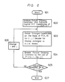
- Fig. 4 the CPU l0 reads out a picture drawing command written on a disk, not shown, in the form of a bit sequence, through the floppy disk interface l6 and stores the picture drawing command in the work RAM l2. Then, at step 402, the CPU l0 analyzes the operand of the picture drawing command, calculates logical X - Y coordinates (on the unit screen), and obtains coordinates of a certain point P (x, y) on the screen, as shown in Fig. 5A.
- the program then proceeds to step 404 whereat it is judged whether or not the value X obtained at step 403 satisfies 0 ⁇ X ⁇ l. If the answer at step 404 is no, the program proceeds to step 407 to be terminated, since the picture drawing cannot be effected unless X satisfies the above condition, 0 ⁇ X ⁇ l.
- step 404 determines whether or not the value Y obtained at step 403 satisfies 0 ⁇ Y ⁇ l. If the answer at step 405 is no, the program proceeds to step 407 to be terminated, since the picture drawing cannot be effected unless Y satisfies the above condition, 0 ⁇ Y ⁇ l. If the answer at step 405 is yes (0 ⁇ Y ⁇ l is satisfied), then the program proceeds to step 406 wherein the values of the coordinates of the point P is stored at a predetermined address in the video RAM l3.
- An address V-RAMadd at a predetermined position in the video RAM l3 is determined by the following equation as shown in Fig. 5B.
- V-RAMadd ⁇ y X max + ⁇ x
- Fig. 5B shows the screen of the display device l9, each pixel of which corresponds to each address in the video RAM l3.
- X max and Y max respectively represent, for example, 256 and 200 pixels.
- the point P of the enlarged or reduced coordinates is drawn at the point P′ expressed by ( ⁇ x, ⁇ y) in Fig. 5B.
- the information indicative of the enlarged or reduced coordinates thus stored in the video RAM l3 is read out therefrom under the control of the CRT controller 30.
- the information is added with the information representative of the intensity of color generated by the color palette memory l4, converted into analog signals by the D/A converter l7, supplied to the video signal processing circuit l8 to be transformed into R, G, and B color signals, and then displayed on the screen of the display device l9.
- the information indicative of enlargement or reduction information read from the video RAM l3 is added with an ID (identification) number corresponding to each of the decoders, and then supplied to the decoders 3A to 3I through the AUX port of the I/O interface l5.
- Each of the decoders 3A to 3I fetches the information having the ID number corresponding thereto, decodes the information, and supplies the decoded information to the corresponding one of the display devices 4A to 4I to display the information on the screen of the corresponding display device. In this way, it is possible to display a large single image or picture by using all the display devices 4A to 4I if information supplied to the decoders 3A to 3I are enlargement information.
- the same single image can be displayed on each of the display devices 4A to 4I if information supplied to the decoders 3A to 3I are reduction information. It will be understood that there is no limitation on display manners. Therefore, it is possible to display a medium sized image by simultaneously using e.g. the display devices 4A, 4B, 4D, and 4E and the same image is displayed by each of the other display devices, i.e. a combination of the medium sized image and the small images. It is also possible that a small image is inserted after a large single image is displayed by using all the display devices.
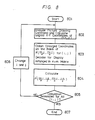
- the data conversion program is started at step 60l, whereat a picture drawing command written on the floppy-disk in the form of a bit sequence is read out by the CPU l0 through the floppy disk interface l6 and stored in the work RAM l2. Then, the CPU l0 analyzes the operand of the picture drawing command, calculates logical X - Y coordinates, and obtain values of a point P (x, y) on the X - Y coordinates at step 602.
- enlarged coordinates are obtained on the basis of a point P′ (nx-i, my-j), wherein the coordinates are those of a (i, j) decoder for one of display devices arranged in n (in the horizontal or row direction) x m (in the vertical or column direction) matrix.
- the value i ranges from 0 to n-l, and the value j from 0 to m-l.
- the picture drawing command is encoded by the use of P′ (nx-i, my-j). That is, the enlarged X - Y coordinates are generated as an ordinary picture drawing command, so that it is not necessary that the decoders are operated without consideration of the enlargement. An enlarged display can be obtained if the decoders are normally operated.
- step 605 it is judged whether or not the calculation is made for all the (i, j), that is, whether or not data to be supplied to all the decoders are converted to data for enlarged display. If the answer is no, the program proceeds to step 606 wherein the values i and j are changed and then, the above described procedure from step 603 to step 604 is repeated. If the answer at step 605 is yes, that is, when the calculation is made for all the (i, j), the program proceeds to step 607 to be terminated.
- reference numerals D0 to D8 correspond to the decoders 3A to 3I.
- the values i and j respectively represent units of muximum number of pixels in the horizontal and vertical directions.
- a unit of the muximum number of pixels in the horizontal direction may consists of 256 pixels, and that in the vertical direction 200 pixels. These values range from 0 to 2, respectively.
- the decoder corresponding to D0 is represented by (0, 0); the decoder corresponding to Dl by (l, 0); the decoder corresponding to D2 by (2, 0); the decoder corresponding to D3 by (0, l); the decoder corresponding to D4 by (l, l); the decoder corresponding to D5 by (2, l); the decoder corresponding to D6 by (0, 2); the decoder corresponding to D7 by (l, 2); and the decoder corresponding to D8 by (2, 2).
- the coordinates of the original data P (x, y) are converted to P′ (nx-i, my-j) for the respective decoders as follows: Decoder corresponding to D0 ...
- the command for drawing a line from a point (x1, y1) to a point (x2, y2) corresponds to those for drawing a line from a point (3x1, 3y1) to a point (3x2, 3y2) for the decoder corresponding to D0; a line from a point (3x-l, 3y) to a point (3x2-l, 3y2) for the decoder corresponding to Dl; a line from a point (3x1-2, 3y1-2) to a point (3x2-2, 3y2-2) for the decoder corresponding to D8.
- ID jn + i.
- ID number of the decoder (0, 0) is 0, that of the decoder (l, 0) is l, ... and that of the decoder (2,2) is 8.
- bezels of the display devices propose a problem. It is desirable that even if there are bezels, an image can be displayed on a plurality of the display devices as if there are no bezels, that is, the bezels are not conspicuous. When a single image is displayed over a plurality of display devices, discrepancies or steps inevitably occur at bezels between adjacent display devices. Therefore, the image, as a whole, is unnaturally displayed.
- the bezel correction program is started at step 80l, whereat certain coordinates written on the disk in the form of a bit sequence are read by the CPU l0 through the floppy disk interface l6 and stored in the work RAM l2.
- the CPU l0 analyzes the picture drawing command, calculates the logical X - Y coordinates, and obtains the coordinates of a point P (x, y) at step 802.
- step 803 the enlarged X - Y coordinates of a point are calculated, where a display ratio satisfies 0 ⁇ ⁇ ⁇ l.
- the X - Y coordinates are data for a decoder (i, j) corresponding to one of the display devices formed into an n x m matrix. Then, the coordinates obtained at step 803 are shifted by in the direction of the origin to obtain coordinates at step 804.
- step 805 it is judged whether or not the calculation is made for all the (i, j), that is, whether or not the shifted coordinates P ⁇ as mentioned above are calculated for all the decoders. If the answer at step 805 is no, the program proceeds to step 806 wherein the values of i and j are changed. Then, the procedure from step 802 to step 804 is repeated. On the other hand, if the answer at step 805 is yes (the above calculaiton is carried out for all the (i, j)), the program proceeds to step 807 to be terminated.
- FIG. 9A and 9B designates a physical display area of a display device, b a frame including a border and bezel portions, and c a line drawn over two adjacent display devices.
- a designates a physical display area of a display device
- b a frame including a border and bezel portions
- c a line drawn over two adjacent display devices.
- step l0l An assignment program is started at step l0l.
- the decoder 3A checks whether or not a data sequence for an ID number assignment as shown in Fig. ll is transmitted from the controller l.
- step l03 it is judged at step l03 whether or not information transmitted from the controller l is a data sequence for ID number assignment. If the answer at step l03 is no, the program proceeds to step l06 to be terminated. On the contrary, if the answer at step l03 is yes, the program proceeds to step l04 whereat the decoder 3A stores therein an ID number included in the data sequence as its own ID number and is set at its initial value.
- the decoder 3A increments its own ID number by l and transmits from its AUX port the incremented ID number as the ID number assigned to the next decoder, i.e. the decoder 3B. Then, the program is terminated at step l06.
- the decoder 3B stores therein the ID number transmitted from the decoder 3A as its own ID number and is set at its initial value. Then, the decoder 3B increments its own ID number by l and transmits from its AUX port the incremented ID number as the ID number assigned to the next decoder 3C. The same procedure is repeated for the decoders 3D to 3I, and thereby the assignment of the ID number to all the decoders 3A to 3I is completed.
- the synchronization program for the controller l is started at step 20l.
- the controller l sets the synchronizing control signal outputted from the I/O interface l5 at one of the two levels, e.g. Low level at step 202.
- the controller l transmits all data to the decoders 3A to 3I.
- the controller l sets the synchronizing control signal outputted from the I/O interface l5 at the other level, e.g. High level after all the data are completely transmitted to the decoders.
- the program is terminated at step 205.
- each decoder receives data through its COM port at step 302 and delivers the received data through its AUX port at step 303. It is judged at step 304 whether or not the synchronizing control signal supplied from the I/O interface l5 of the controller l to the I/O interface 25 of each of the decoders is at High level. If the answer at step 304 is no, that is, the synchronizing control signal is not in High level, the program returns to step 302.
- step 305 the received data is decoded by each decoder.
- step 306 it is judged whether or not the data transmission is terminated. If the answer is no, the program returns to step 304. On the contrary, if the answer is yes, the program proceeds to step 307 to be terminated.
- the decoders 3A to 3I receive data but do not decode them while the synchronizing control signal is at Low level and that when the synchronizing control signal becomes High level, all the decoders 3A to 3I start at the same time the decoding of the data received.
- the controller l When data overflow is detected by one of serially connected decoders, the decoder commands the preceding decoder to stop the outputting of the data.
- the controller l is provided with a buffer TC for data tansmission and a buffer TR for data reception for the COM port and a buffer TA for data transmission and a buffer RA for data reception for the AUX port.
- the buffers TC, TR, TA, and RA are allocated on the work RAM l2, and only the transmission buffer TA and the reception buffer RA for the AUX port appear in Fig. l4.
- each decoder is provided with a transmission buffer TC and a reception buffer RC for the COM port and a transmission buffer TA and a reception buffer RA for the AUX port, all of which are allocated on the work RAM 22.
- the data in the transmission buffer TA for the AUX port of the controller l is transmitted to the reception buffer RC for the COM port of the decoder 3A.
- the data in the transmission buffer TC for the COM port of the decoder 3A is transmitted to the reception buffer RA for the AUX port of the controller l. Namely, the data are bi-directionally transmitted between the controller l and the decoder 3A.
- the data in the transmission port TA for the AUX port of the decoder 3A is transmitted to the reception buffer RC for the COM port of the decoder 3B, and the data in the transmission buffer TC for the COM port of the decoder 3B is transmitted to the reception buffer RA for the AUX port of the decoder 3A, that is, the bi-directional transmission of the data is effected also between the decoders 3A and 3B.
- the other decoders are constructed such that the bi-directional data transmission can be effected between respective adjacent decoders.
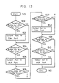
- a transmission program is started at step 50l.
- step 502 it is judged at step 502 whether or not the reception buffer RC for the COM port of the decoder 3B is full, that is, whether or not the reception buffer RC is overflowed with transmitted data. If the answer is yes at step 502, the program proceeds to step 503 whereat a transmission stop singal X off outputted to the transmission buffer TC for the COM port of the decoder 3B.
- the transmission stop signal X off is then received by the reception buffer RA for the AUX port of the preceding decoder 3A, so that the decoder 3A stops the transmitting of the data to the decoder 3B.
- step 504 If the answer at step 502 is no, that is the reception buffer RC of the decoder 3B is not full, the program jumps to step 504. Then, it is judged at step 504 whether or not the reception buffer RA for the AUX port of the decoder 3B is full. If the answer is yes, the program proceeds to step 505 whereat a transmission stop signal X off is outputted to the transmission buffer TA for the AUX port of the decoder 3B. The signal X off is then transmitted to the transmission buffer RC for the COM port of the next decoder 3C, whereby the decoder 3C stops the transmitting of the data to the decoder 3B. If the answer at the step 504 is no, that is, if the buffer RA is not full, the program jumps to step 506.
- step 506 it is judged whether or not the transmission stop signal x off is outputted to the transmission buffer TC for the COM port of the decoder 3B. If the answer is yes, the program proceeds to step 507 whereat it is judged whether or not the transmission buffer RC for the COM port of the decoder 3B has a free or vacant area. If the answer at step 507 is yes, that is, if the transmission buffer RC has a vacant area, the transmission buffer TC for the COM port of the decoder 3B is supplied with a transmission resuming signal X on at step 508.
- the signal X on is then received by the reception buffer RA for the AUX port of the preceding decoder 3A, and thereby the decoder 3A resumes the data transmission to the decoder 3B. If the answer at step 506 or 507 is no, that is, if the transmission signal X off is not outputted or if the reception buffer RC does not have free area, the program jumps to step 509.
- step 509 it is judged at step 509 whether or not the transmission stop signal X off is outputted to the transmission buffer TA for the AUX port of the decoder 3B. If the answer is yes, the program proceeds to step 5l0 whereat it is judged whether or not the reception buffer RA for the AUX port of the decoder 3B has free area. If the answer at step 5l0 is yes, the transmission resuming signal X on is outputted to the transmission buffer TA for the AUX port of the decoder 3B at step 5ll. The signal X on is then received by the reception buffer RC for the COM port of the next decoder 3C, whereby the decoder 3C resumes the data transmission to the decoder 3B.
- step 5l2 the program proceeds to step 5l2 to be terminated. If the answer at step 509 or 5l0 is no, that is, if the transmission stop signal X off is not outputted or if the reception buffer RA does not have free area, the program jumps to step 5l2 to be terminated.
- the identification number is inserted in a predetermined portion of the data sequence generated by the information generating means, and the first terminal of a plurality of serially connected terminals is set at the initial value by the identification number supplied from the information generating means and produces and transmits a new identification number for the terminal at the next stage, so that each of a plurality of the serially connected terminals can be set at its initial value by the assigned identification number through substantially one transmission line, whereby the circuit construction of the system can be simplified. Also, it is not necessary to provide the information generating means with ransmission ports for every terminal but only one transmission port for the first terminal, so that it is possible to simplify the circuit configuration of the information generating means.
Landscapes
- Engineering & Computer Science (AREA)
- Theoretical Computer Science (AREA)
- Signal Processing (AREA)
- Human Computer Interaction (AREA)
- Physics & Mathematics (AREA)
- General Engineering & Computer Science (AREA)
- General Physics & Mathematics (AREA)
- Multimedia (AREA)
- Controls And Circuits For Display Device (AREA)
- Studio Circuits (AREA)
- Transforming Electric Information Into Light Information (AREA)
- Control Of Indicators Other Than Cathode Ray Tubes (AREA)
Applications Claiming Priority (2)
| Application Number | Priority Date | Filing Date | Title |
|---|---|---|---|
| JP61004760A JP2513180B2 (ja) | 1986-01-13 | 1986-01-13 | ビデオテックス表示装置 |
| JP4760/86 | 1986-01-17 |
Publications (2)
| Publication Number | Publication Date |
|---|---|
| EP0230241A1 true EP0230241A1 (fr) | 1987-07-29 |
| EP0230241B1 EP0230241B1 (fr) | 1991-06-12 |
Family
ID=11592844
Family Applications (1)
| Application Number | Title | Priority Date | Filing Date |
|---|---|---|---|
| EP87100262A Expired - Lifetime EP0230241B1 (fr) | 1986-01-13 | 1987-01-12 | Système indicateur multiple |
Country Status (5)
| Country | Link |
|---|---|
| US (1) | US4800376A (fr) |
| EP (1) | EP0230241B1 (fr) |
| JP (1) | JP2513180B2 (fr) |
| KR (1) | KR940008840B1 (fr) |
| DE (1) | DE3770646D1 (fr) |
Cited By (5)
| Publication number | Priority date | Publication date | Assignee | Title |
|---|---|---|---|---|
| EP0309355A1 (fr) * | 1987-09-23 | 1989-03-29 | Olivier Auber | Système de communication vidéo interactif |
| WO1991013518A1 (fr) * | 1990-02-16 | 1991-09-05 | Madimelia (Overseas) Limited | Systeme d'affichage |
| EP0899651A3 (fr) * | 1997-08-29 | 2000-02-23 | Xerox Corporation | Affichages par zone dynamiquement réallouable |
| EP1612657A3 (fr) * | 2004-07-02 | 2009-04-01 | Microsoft Corporation | Système et procédé pour déterminer des différences d' affichage entre moniteurs dans des systèmes d' ordinateur à moniteurs multiples |
| US7948449B2 (en) | 2005-03-31 | 2011-05-24 | Sega Corporation | Display control program executed in game machine |
Families Citing this family (81)
| Publication number | Priority date | Publication date | Assignee | Title |
|---|---|---|---|---|
| US4991121A (en) * | 1985-10-16 | 1991-02-05 | Fuji Photo Film Co., Ltd. | Image display system |
| EP0635970B1 (fr) * | 1988-01-08 | 2000-04-12 | Fuji Photo Film Co., Ltd. | Appareil pour l'analyse de films en couleurs |
| JPH01264482A (ja) * | 1988-04-15 | 1989-10-20 | Pioneer Electron Corp | テレビジョン信号受信装置 |
| US5111303A (en) * | 1989-02-27 | 1992-05-05 | Pioneer Electronic Corporation | Video signal recording system and picture display system in a high-definition television system |
| US5287179A (en) * | 1989-02-27 | 1994-02-15 | Pioneer Electronic Corporation | Image display system |
| US5010413A (en) * | 1989-10-10 | 1991-04-23 | Imtech International, Inc. | Method and apparatus for displaying an enlarged image on multiple monitors to form a composite image |
| JP2947840B2 (ja) * | 1989-12-22 | 1999-09-13 | 株式会社日立製作所 | プラント運転監視装置 |
| JPH07105914B2 (ja) * | 1990-05-23 | 1995-11-13 | 三菱電機株式会社 | 画像出力制御装置 |
| US5031046A (en) * | 1990-06-01 | 1991-07-09 | Preh-Werke Gmbh & Co. Kg | Remote control device for a television set |
| FR2668846B1 (fr) * | 1990-11-07 | 1993-02-12 | Rasec Communication Sa | Dispositif d'affichage electronique de donnees. |
| US5321505A (en) * | 1991-01-11 | 1994-06-14 | Microelectronics & Computer Technology Corporation | Computer scalable visualization system |
| CA2060361A1 (fr) * | 1991-01-31 | 1992-08-01 | Masao Fukuda | Dispositif de commande d'affichage |
| JP2501965B2 (ja) * | 1991-02-12 | 1996-05-29 | パイオニア株式会社 | デ―タ転送制御装置 |
| USD340049S (en) | 1991-03-19 | 1993-10-05 | Liljenwall Robert J | Outdoor video display unit |
| US5329444A (en) * | 1991-04-26 | 1994-07-12 | Shimizu Construction Co., Ltd. | Work management system employing electronic board |
| US5374940A (en) * | 1991-06-04 | 1994-12-20 | The University Of Rochester | System for operating a plurality of graphics displays from a single computer |
| GB9201949D0 (en) * | 1992-01-30 | 1992-03-18 | Jenkin Michael | Large-scale,touch-sensitive video display |
| JP2935307B2 (ja) * | 1992-02-20 | 1999-08-16 | 株式会社日立製作所 | ディスプレイ |
| JPH05257437A (ja) * | 1992-03-13 | 1993-10-08 | Nec Corp | 表示装置 |
| US6469746B1 (en) * | 1992-12-28 | 2002-10-22 | Sanyo Electric Co., Ltd. | Multi-vision screen adapter |
| JP3334211B2 (ja) * | 1993-02-10 | 2002-10-15 | 株式会社日立製作所 | ディスプレイ |
| DE4447944B4 (de) * | 1993-02-10 | 2004-11-11 | Hitachi, Ltd. | Informationsausgabesystem |
| JPH07146671A (ja) * | 1993-06-16 | 1995-06-06 | Mitsubishi Electric Corp | 大型映像表示装置 |
| US5805117A (en) * | 1994-05-12 | 1998-09-08 | Samsung Electronics Co., Ltd. | Large area tiled modular display system |
| US6025840A (en) * | 1995-09-27 | 2000-02-15 | Cirrus Logic, Inc. | Circuits, systems and methods for memory mapping and display control systems using the same |
| JP3339284B2 (ja) * | 1996-01-29 | 2002-10-28 | 三菱電機株式会社 | 大画面表示方式 |
| JP2962348B2 (ja) * | 1996-02-08 | 1999-10-12 | 日本電気株式会社 | 画像符号変換方式 |
| US5986622A (en) * | 1996-05-24 | 1999-11-16 | Lucent Technologies Inc. | Panel display of multiple display units for multiple signal sources |
| US6680714B2 (en) * | 1996-06-14 | 2004-01-20 | Charles E. Wilmore | Interactive multi-user display arrangement for displaying goods and services |
| JPH11161590A (ja) * | 1997-11-27 | 1999-06-18 | Hitachi Ltd | 情報視聴装置 |
| USD415744S (en) * | 1998-06-10 | 1999-10-26 | Pelco | Flat screen monitor with multiple screens |
| JP2004500731A (ja) * | 1998-06-18 | 2004-01-08 | ソニー エレクトロニクス インク | 複数のディスプレイ装置に亘ってビデオ及び/又はグラフィック画像を分割し、スケーリングし、表示する方法及び装置 |
| US6593937B2 (en) | 1998-06-18 | 2003-07-15 | Sony Corporation | Method of and apparatus for handling high bandwidth on-screen-display graphics data over a distributed IEEE 1394 network utilizing an isochronous data transmission format |
| US6377276B1 (en) | 1998-06-18 | 2002-04-23 | Sony Corporation | Bitmap animation of on-screen-display graphics over a distributed network and a clipping region having a visible window |
| US20010026533A1 (en) * | 1998-07-06 | 2001-10-04 | Andreas Schwager | Method to perform a scheduled action of network devices |
| US7008324B1 (en) * | 1998-10-01 | 2006-03-07 | Paltronics, Inc. | Gaming device video display system |
| US6343006B1 (en) | 1998-11-20 | 2002-01-29 | Jerry Moscovitch | Computer display screen system and adjustable screen mount, and swinging screens therefor |
| US6567092B1 (en) * | 1999-02-10 | 2003-05-20 | Microsoft Corporation | Method for interfacing to ultra-high resolution output devices |
| US7885340B2 (en) * | 1999-04-27 | 2011-02-08 | Realnetworks, Inc. | System and method for generating multiple synchronized encoded representations of media data |
| JP2000338941A (ja) * | 1999-05-27 | 2000-12-08 | Seiko Epson Corp | 投射型表示装置 |
| US6690337B1 (en) | 1999-06-09 | 2004-02-10 | Panoram Technologies, Inc. | Multi-panel video display |
| EP1208697A4 (fr) * | 1999-06-09 | 2006-03-01 | Panoram Technologies Inc | Affichage video a panneaux multiples |
| US20020151360A1 (en) * | 1999-09-10 | 2002-10-17 | Durham Timothy J. | Gaming machine having a controller for controlling multiple displays |
| US6254481B1 (en) | 1999-09-10 | 2001-07-03 | Wms Gaming Inc. | Gaming machine with unified image on multiple video displays |
| US20060009286A1 (en) * | 1999-09-10 | 2006-01-12 | Wms Gaming Inc. | Gaming machine having a controller for conrolling multiple displays |
| JP4564613B2 (ja) * | 1999-10-19 | 2010-10-20 | キヤノン株式会社 | 画像処理装置、テレビジョン受像機、及び、画像処理方法 |
| WO2001035197A1 (fr) | 1999-11-12 | 2001-05-17 | Mass Engineered Design | Systeme lcd horizontal a trois ecrans |
| US6816129B1 (en) * | 1999-12-21 | 2004-11-09 | International Business Machines Corporation | Multiple display device for use with existing personal computer systems |
| CA2298358A1 (fr) * | 2000-02-11 | 2001-08-11 | Pixel Systems Inc. | Methode et appareil pour l'affichage d'images selectionnees a des moments selectionnes |
| DE10041436A1 (de) * | 2000-08-23 | 2002-03-14 | Infineon Technologies Ag | Datensichtanordnung und Verfahren zum Ermitteln der örtlichen Position einer Datensichteinheit innerhalb einer Datensichtanordnung mit einer Vielzahl von Datensichteinheiten |
| US7170468B2 (en) | 2001-02-21 | 2007-01-30 | International Business Machines Corporation | Collaborative tablet computer |
| US20040145535A1 (en) * | 2001-03-23 | 2004-07-29 | Uwe Gerk | Process control system with image representation system |
| US6870519B2 (en) * | 2001-03-28 | 2005-03-22 | Intel Corporation | Methods for tiling multiple display elements to form a single display |
| US20020171667A1 (en) * | 2001-05-15 | 2002-11-21 | Motorola, Inc. | Method and apparatus for processing data including an image for presentation on a display |
| JP4926350B2 (ja) * | 2001-09-14 | 2012-05-09 | 株式会社神戸製鋼所 | 防音表面部材 |
| KR100435114B1 (ko) * | 2001-12-20 | 2004-06-09 | 삼성전자주식회사 | 액정디스플레이장치 |
| WO2003058952A1 (fr) * | 2001-12-28 | 2003-07-17 | Sony Corporation | Appareil d'affichage et procede de commande |
| US7512454B1 (en) | 2002-05-31 | 2009-03-31 | Advanced Micro Devices, Inc. | Display unit with processor and communication controller |
| US20030225474A1 (en) * | 2002-05-31 | 2003-12-04 | Gustavo Mata | Specialization of active software agents in an automated manufacturing environment |
| KR20040013957A (ko) * | 2002-08-09 | 2004-02-14 | 엘지전자 주식회사 | 멀티비전 및 그 화면 구현 방법 |
| KR100449743B1 (ko) * | 2002-10-04 | 2004-09-22 | 삼성전자주식회사 | 상호 진단 기능을 가지는 Chained영상 표시 장치 |
| KR100465173B1 (ko) * | 2002-11-18 | 2005-01-13 | 삼성전자주식회사 | 화면분할 기능을 갖는 영상디스플레이장치 |
| JP2004226513A (ja) * | 2003-01-21 | 2004-08-12 | Pioneer Electronic Corp | マルチディスプレイ映像表示システム |
| US7034776B1 (en) * | 2003-04-08 | 2006-04-25 | Microsoft Corporation | Video division detection methods and systems |
| DE10334516B4 (de) | 2003-07-29 | 2006-06-14 | Sorin Group Deutschland Gmbh | Anzeige- und Bedienvorrichtung für medizintechnische Geräte und Anzeige-/Bedieneinheit dafür |
| US20050130732A1 (en) * | 2003-12-12 | 2005-06-16 | Rothschild Wayne H. | Random bonus delivery mechanism for a gaming system |
| US20060028398A1 (en) * | 2004-07-23 | 2006-02-09 | Willmore Charles E | Wireless interactive multi-user display system and method |
| US20080275582A1 (en) * | 2004-11-19 | 2008-11-06 | Nettles Steven C | Scheduling AMHS pickup and delivery ahead of schedule |
| US20070035668A1 (en) * | 2005-08-11 | 2007-02-15 | Sony Corporation | Method of routing an audio/video signal from a television's internal tuner to a remote device |
| EP1763243A3 (fr) * | 2005-09-09 | 2008-03-26 | LG Electronics Inc. | Methode et système de capture et d'affichage d'image |
| US20070150924A1 (en) * | 2005-12-06 | 2007-06-28 | Pioneer Corporation | Image display control apparatus, image display system, image display control method, computer program product, sub-display control apparatus for image display system, and image display method |
| KR100738497B1 (ko) * | 2006-04-18 | 2007-07-11 | 인포스퀘어 주식회사 | 멀티싱크 영상 출력 시스템 |
| JP5119655B2 (ja) * | 2006-12-13 | 2013-01-16 | 株式会社日立製作所 | マルチスクリーン表示装置 |
| US7753777B1 (en) | 2007-01-03 | 2010-07-13 | Gregg Giuffria | Device and method for conducting a game of chance |
| US20110112356A1 (en) * | 2009-11-12 | 2011-05-12 | Mark Ellery Ogram | Dementia treatment |
| US8587187B2 (en) | 2010-12-06 | 2013-11-19 | Byoung GU Cho | Light diffusion of visible edge lines in a multi-dimensional modular display |
| JP2012100891A (ja) | 2010-11-10 | 2012-05-31 | Universal Entertainment Corp | ゲーミングマシン |
| WO2013095512A1 (fr) * | 2011-12-22 | 2013-06-27 | Intel Corporation | Plateforme de divertissement commune |
| CN105845036A (zh) * | 2015-01-14 | 2016-08-10 | 丁炜慷 | 一种拼接后“像素全覆盖”的“全无缝”显示幕墙系统 |
| KR101675804B1 (ko) * | 2015-05-27 | 2016-11-15 | 한화테크윈 주식회사 | 비디오 월(video wall)이 형성되는 감시 시스템 |
| CN114302149B (zh) * | 2021-12-24 | 2023-05-09 | 北京淳中科技股份有限公司 | 一种音视频传输方法、装置及系统 |
Citations (3)
| Publication number | Priority date | Publication date | Assignee | Title |
|---|---|---|---|---|
| GB2092346A (en) * | 1980-07-25 | 1982-08-11 | Mitsubishi Electric Corp | Display apparatus |
| EP0074696A1 (fr) * | 1981-09-10 | 1983-03-23 | Vidcom Rentservice B.V. | Système d'affichage d'information |
| DE3222266A1 (de) * | 1982-06-10 | 1983-12-15 | Karl Heinz 2000 Hamburg Krings | Demonstrationswand |
Family Cites Families (8)
| Publication number | Priority date | Publication date | Assignee | Title |
|---|---|---|---|---|
| US4112423A (en) * | 1976-09-13 | 1978-09-05 | Kelsey-Hayes Co. | Dual-screen data display terminal for data processing units |
| GB2123656B (en) * | 1982-06-09 | 1987-02-18 | Tatsumi Denshi Kogyo Kk | A method and an apparatus for displaying a unified picture on crt screens of multiple displaying devices |
| FR2549671B1 (fr) * | 1983-07-22 | 1987-05-22 | Thomson Csf | Dispositif d'affichage d'une image de television de grandes dimensions et recepteur de television comportant un tel dispositif |
| GB2148077B (en) * | 1983-09-20 | 1987-08-12 | Rees Elwyn | Video display control system |
| CA1239468A (fr) * | 1984-01-13 | 1988-07-19 | Yuji Watanabe | Systeme d'affichage video |
| JPH0614717B2 (ja) * | 1984-05-11 | 1994-02-23 | 三菱電機株式会社 | 映像デ−タ転送方式 |
| US4694293A (en) * | 1984-09-18 | 1987-09-15 | Nippon Gakki Seizo Kabushiki Kaisha | Data transmission system |
| JPH0761140B2 (ja) * | 1985-05-21 | 1995-06-28 | ティアツク株式会社 | マルチ映像表示方式 |
-
1986
- 1986-01-13 JP JP61004760A patent/JP2513180B2/ja not_active Expired - Fee Related
- 1986-12-23 US US06/945,797 patent/US4800376A/en not_active Expired - Lifetime
- 1986-12-29 KR KR1019860011433A patent/KR940008840B1/ko not_active Expired - Lifetime
-
1987
- 1987-01-12 EP EP87100262A patent/EP0230241B1/fr not_active Expired - Lifetime
- 1987-01-12 DE DE8787100262T patent/DE3770646D1/de not_active Expired - Lifetime
Patent Citations (3)
| Publication number | Priority date | Publication date | Assignee | Title |
|---|---|---|---|---|
| GB2092346A (en) * | 1980-07-25 | 1982-08-11 | Mitsubishi Electric Corp | Display apparatus |
| EP0074696A1 (fr) * | 1981-09-10 | 1983-03-23 | Vidcom Rentservice B.V. | Système d'affichage d'information |
| DE3222266A1 (de) * | 1982-06-10 | 1983-12-15 | Karl Heinz 2000 Hamburg Krings | Demonstrationswand |
Non-Patent Citations (1)
| Title |
|---|
| FUNKSCHAU, 14/1982, Munchen HEINZ W. KRAMER "Gross-Farbbildschirm" pages 65-67 * |
Cited By (7)
| Publication number | Priority date | Publication date | Assignee | Title |
|---|---|---|---|---|
| EP0309355A1 (fr) * | 1987-09-23 | 1989-03-29 | Olivier Auber | Système de communication vidéo interactif |
| WO1991013518A1 (fr) * | 1990-02-16 | 1991-09-05 | Madimelia (Overseas) Limited | Systeme d'affichage |
| US5361078A (en) * | 1990-02-16 | 1994-11-01 | Nadimelia Limited | Multiple screen graphics display |
| EP0899651A3 (fr) * | 1997-08-29 | 2000-02-23 | Xerox Corporation | Affichages par zone dynamiquement réallouable |
| US6340957B1 (en) | 1997-08-29 | 2002-01-22 | Xerox Corporation | Dynamically relocatable tileable displays |
| EP1612657A3 (fr) * | 2004-07-02 | 2009-04-01 | Microsoft Corporation | Système et procédé pour déterminer des différences d' affichage entre moniteurs dans des systèmes d' ordinateur à moniteurs multiples |
| US7948449B2 (en) | 2005-03-31 | 2011-05-24 | Sega Corporation | Display control program executed in game machine |
Also Published As
| Publication number | Publication date |
|---|---|
| EP0230241B1 (fr) | 1991-06-12 |
| DE3770646D1 (de) | 1991-07-18 |
| KR870007627A (ko) | 1987-08-20 |
| JPS62163478A (ja) | 1987-07-20 |
| KR940008840B1 (ko) | 1994-09-26 |
| JP2513180B2 (ja) | 1996-07-03 |
| US4800376A (en) | 1989-01-24 |
Similar Documents
| Publication | Publication Date | Title |
|---|---|---|
| US4800376A (en) | Multiple display system | |
| KR100197837B1 (ko) | 더블스크린을 이용한 정보 및 외부신호 표시장치 | |
| US5559954A (en) | Method & apparatus for displaying pixels from a multi-format frame buffer | |
| JP2615841B2 (ja) | 静止画編集装置 | |
| EP0587342A1 (fr) | Méthode et système pour la commande indépendante de fenêtres multiples dans un système de visualisation graphique | |
| US20030011606A1 (en) | Video data processing device and video data display device | |
| JPH0832904A (ja) | マルチパネル表示システム | |
| JP2006119509A (ja) | 表示装置及びその表示方法 | |
| JPH06332843A (ja) | 動画映像データ転送装置およびコンピュータシステム | |
| US7148866B2 (en) | Liquid crystal display apparatus and a method of controlling the same | |
| US6782134B2 (en) | Transmission apparatus of video information, transmission system of video information and transmission method of video information | |
| US5923322A (en) | Enhanced feature connector for an overlay board | |
| JPH0454789A (ja) | テレビ画像表示装置 | |
| JPS62163481A (ja) | ビデオテツクスのマルチデイスプレイ装置 | |
| US20030160748A1 (en) | Display control circuit, semiconductor device, and portable device | |
| JP2003323168A (ja) | プロジェクタ装置 | |
| EP0153749B1 (fr) | Système de transmission numérique pour la transmission et l'affichage d'images et de données | |
| JPS61173594A (ja) | ハ−ドコピ−出力機能付静止画像表示装置 | |
| JP3474104B2 (ja) | スキャンコンバータ | |
| EP0414311B1 (fr) | Dispositif de reproduction d'images et circuit de traitement de signaux vidéo | |
| JP2894232B2 (ja) | 文字情報重畳装置 | |
| JPS62163164A (ja) | マルチプロセツサ | |
| JP3204123B2 (ja) | オーバレイ方式 | |
| JPH1152915A (ja) | 液晶ディスプレイ接続システム、グラフィックボード及び液晶ディスプレイ | |
| JPH0683417B2 (ja) | ビデオテツクス表示装置 |
Legal Events
| Date | Code | Title | Description |
|---|---|---|---|
| PUAI | Public reference made under article 153(3) epc to a published international application that has entered the european phase |
Free format text: ORIGINAL CODE: 0009012 |
|
| AK | Designated contracting states |
Kind code of ref document: A1 Designated state(s): DE FR GB NL |
|
| 17P | Request for examination filed |
Effective date: 19880125 |
|
| 17Q | First examination report despatched |
Effective date: 19891222 |
|
| GRAA | (expected) grant |
Free format text: ORIGINAL CODE: 0009210 |
|
| AK | Designated contracting states |
Kind code of ref document: B1 Designated state(s): DE FR GB NL |
|
| REF | Corresponds to: |
Ref document number: 3770646 Country of ref document: DE Date of ref document: 19910718 |
|
| ET | Fr: translation filed | ||
| PLBE | No opposition filed within time limit |
Free format text: ORIGINAL CODE: 0009261 |
|
| STAA | Information on the status of an ep patent application or granted ep patent |
Free format text: STATUS: NO OPPOSITION FILED WITHIN TIME LIMIT |
|
| 26N | No opposition filed | ||
| REG | Reference to a national code |
Ref country code: GB Ref legal event code: IF02 |
|
| PGFP | Annual fee paid to national office [announced via postgrant information from national office to epo] |
Ref country code: FR Payment date: 20020110 Year of fee payment: 16 |
|
| PGFP | Annual fee paid to national office [announced via postgrant information from national office to epo] |
Ref country code: GB Payment date: 20020116 Year of fee payment: 16 |
|
| PGFP | Annual fee paid to national office [announced via postgrant information from national office to epo] |
Ref country code: NL Payment date: 20020131 Year of fee payment: 16 |
|
| PGFP | Annual fee paid to national office [announced via postgrant information from national office to epo] |
Ref country code: DE Payment date: 20020212 Year of fee payment: 16 |
|
| PG25 | Lapsed in a contracting state [announced via postgrant information from national office to epo] |
Ref country code: GB Free format text: LAPSE BECAUSE OF NON-PAYMENT OF DUE FEES Effective date: 20030112 |
|
| PG25 | Lapsed in a contracting state [announced via postgrant information from national office to epo] |
Ref country code: NL Free format text: LAPSE BECAUSE OF NON-PAYMENT OF DUE FEES Effective date: 20030801 Ref country code: DE Free format text: LAPSE BECAUSE OF NON-PAYMENT OF DUE FEES Effective date: 20030801 |
|
| GBPC | Gb: european patent ceased through non-payment of renewal fee | ||
| PG25 | Lapsed in a contracting state [announced via postgrant information from national office to epo] |
Ref country code: FR Free format text: LAPSE BECAUSE OF NON-PAYMENT OF DUE FEES Effective date: 20030930 |
|
| NLV4 | Nl: lapsed or anulled due to non-payment of the annual fee |
Effective date: 20030801 |
|
| REG | Reference to a national code |
Ref country code: FR Ref legal event code: ST |