EP0230278A2 - Thyristor avec dispositif d'alimentation intégré d'un circuit défini et procédé pour sa fabrication - Google Patents
Thyristor avec dispositif d'alimentation intégré d'un circuit défini et procédé pour sa fabrication Download PDFInfo
- Publication number
- EP0230278A2 EP0230278A2 EP87100469A EP87100469A EP0230278A2 EP 0230278 A2 EP0230278 A2 EP 0230278A2 EP 87100469 A EP87100469 A EP 87100469A EP 87100469 A EP87100469 A EP 87100469A EP 0230278 A2 EP0230278 A2 EP 0230278A2
- Authority
- EP
- European Patent Office
- Prior art keywords
- base
- thyristor
- emitter
- conductive
- circuit unit
- Prior art date
- Legal status (The legal status is an assumption and is not a legal conclusion. Google has not performed a legal analysis and makes no representation as to the accuracy of the status listed.)
- Withdrawn
Links
Images
Classifications
-
- H—ELECTRICITY
- H10—SEMICONDUCTOR DEVICES; ELECTRIC SOLID-STATE DEVICES NOT OTHERWISE PROVIDED FOR
- H10D—INORGANIC ELECTRIC SEMICONDUCTOR DEVICES
- H10D84/00—Integrated devices formed in or on semiconductor substrates that comprise only semiconducting layers, e.g. on Si wafers or on GaAs-on-Si wafers
- H10D84/101—Integrated devices comprising main components and built-in components, e.g. IGBT having built-in freewheel diode
- H10D84/131—Thyristors having built-in components
Definitions
- the invention relates to a thyristor with an associated circuit unit to be supplied with operating current according to the preamble of claim 1 and to methods for its production.
- a thyristor of this type is known from DE-A-32 26 613.
- the associated circuit unit to be supplied with operating current consists of a light-sensitive switching element which is connected between the conductive assignment and the cathode-side electrode.
- This switching element e.g. a phototransistor, has a relatively low blocking capability and a large photosensitivity that is compatible with it, so that the system consisting of the thyristor and the switching element has both a high ignition sensitivity and a large blocking capability.
- the conductive assignment at high blocking voltages lies in the region of the space charge zone starting from the pn junction between the two base layers and largely filling the approach of the n base. This leads to leakage currents, which may cause an unwanted ignition of the thyristor or make an intended ignition difficult.
- the invention has for its object to provide a thyristor of the type mentioned, in which such leakage currents emanating from the conductive assignment are largely avoided and a safe and controllable Power supply to the assigned circuit unit takes place. This is achieved according to the invention by training according to the characterizing part of patent claim 1.
- the advantage that can be achieved with the invention is, in particular, that the assigned circuit unit is supplied with the required operating variables in a controllable manner, both the maximum operating voltage applied to the circuit unit and the maximum operating current supplied to it by appropriate dimensioning of the second part of the n- Emitter approach are specified.
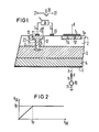
- Fig. 1 is a thyristor with a semiconductor body made of doped semiconductor material, e.g. Silicon, shown, which has four successive layers of alternating conduction types. These are the n-emitter 1, the p-base 2, the n-base 3 and the p-emitter 4.
- the n-emitter 1 is provided with an electrode 5 on the cathode side, the p-emitter 4 with a anode-side electrode 6, the electrodes made of an electrically conductive material, for example Aluminum.
- the electrode 5 is connected to ground via a connection K, the electrode 6 via a connection A and a load resistor R to the upper connection 9 of a voltage source 10, the lower connection 11 of which is connected to ground.
- the n-base has an n-conductive extension 12, which penetrates the p-base 2, extends to the interface 1a of the semiconductor body and is contacted by a conductive coating 13 in the latter.
- the approach 12 is composed of a first part 14 and a second part 15, which is arranged between the part 14 and the n base 3.
- the cross section of the part 15 considered in the boundary surface 1 a can have, for example, a square or rectangular shape, the visible dimension B1 being dimensioned larger than the parallel dimension of the occupancy 13.
- the width of the part 14 measured perpendicular to the image plane is likewise dimensioned larger than the dimension of the occupancy 13 in this direction.
- the cross-sectional dimensions of the second part 15, which also has a square or rectangular cross-section, ie the depth 2a measured in the image plane and the width Z measured perpendicularly to it, are dimensioned smaller than that The dimensions of the part 14.
- the length of the part 15 is denoted by L.
- the n-emitter 1 is provided with emitter-base short-circuits, which consist of projections 16 and 17 of the p-base 2, which penetrate the n-emitter 1 and are contacted by the electrode 5 in the interface 1a.
- the assignment 13 has a connection S which is connected to the first connection of a circuit unit 18 assigned to the thyristor.
- 18, as indicated in FIG. 1 consists of a photo transistor 20, the connections 21 and 22 of which are each connected to S and G, so that the connections S and G are connected to one another via the switching path of 20.
- the second part 15 of the approach 12 can be understood as the channel of a junction field effect transistor (JFET) with a channel depth 2a, a channel length L and a channel width Z, the source connection of which is formed by S and the drain of which is formed by the n-base 3.
- JFET junction field effect transistor
- the p-base surrounding the channel 15 represents a gate area which is contacted by 19 and can be controlled via the connection G. Via the short circuits 16 and 17, G is always at the ground potential of the electrode 5 on the cathode side.
- the connection between S and G is very high-impedance. If the anode voltage V AK is allowed to rise from zero in the direction of positive values, the potential at the connection S and at a point D, which roughly characterizes the transition between the channel 15 and the n base 3, corresponds to the voltage V AK . If V AK reaches a value V P , in which the entire cross section of the channel 15 is filled by the space charge zone, which builds up at the pn junction 23 between the attachment 12 and the p base 2, the circuit points S and D are also at V P. A further increase in V AK , for example to 5000 volts and above, then no longer influences the voltage at S and D. If the voltage V SK , which can be measured between the connections S and K, is plotted against the anode voltage V AK , this fact can be illustrated in accordance with FIG. 2.
- I P V bi mean the impressed voltage at the pn junction between parts 2 and 15 and ⁇ the mobility of the charge carriers in channel 15.
- the approach 12 has the meaning of an integrated power supply part, which can supply the circuit unit 18 with a maximum operating current I DSat when V AK rises above V P. If the light-sensitive switching element in FIG. 18 is illuminated, then a drain current flows in the structure design described, which can be up to 25 mA depending on the light intensity and amplification factor of the circuit unit 18. This is fed to the terminal G of the ignition electrode 19 as an ignition current.
- the light energy that is supplied to the circuit unit 18 for triggering the ignition is substantially less than that which would have to be supplied to the thyristor for direct light ignition.
- the cross-sectional dimensions of the first part 14 of the extension 12 are chosen to be larger than the dimensions of the covering 13, because this ensures that the covering 13 does not come into contact with the space charge zone formed at the pn junction 23. In this way, disturbing leakage currents can be avoided.
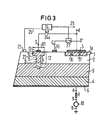
- FIG. 3 shows another exemplary embodiment of the invention, which corresponds completely to the semiconductor structure according to FIG. 1, but differs from FIG. 1 by a different wiring of S, G and K.
- a circuit unit 24 assigned to the thyristor is provided here, which is connected via the integrated power supply part 12 from the at A and K. its load circuit is supplied with operating current.
- 24 denotes a logic circuit which is connected to a temperature sensor 25 attached to the interface 1a via a line 26.
- the temperature sensor 25 delivers, for example, a signal when the semiconductor body of the thyristor has reached or exceeded a maximum permissible temperature.
- This signal is processed in 24 into a switching signal which opens an electronic switch 27, so that an ignition current pulse 28, which is supplied by an ignition circuit, not shown, no longer reaches terminal G.
- the thyristor therefore does not ignite until its temperature has dropped below the maximum permissible value.
- the logic circuit 24 can also be designed as a message logic which, when the critical temperature is reached, transmits a message in this regard to a monitoring point, as indicated by the arrow 29.
- the operating current for the logic circuit 24 is supplied via the connections 24a connected to S and K.
- the thyristor structure according to FIGS. 1 and 3 is produced in a conventional manner by a series of diffusion steps which are carried out using diffusion marks.
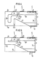
- Fig. 4 shows a modification of this thyristor structure, which can be manufactured more easily.
- a disk made of n-doped semiconductor material, for example silicon, is assumed.
- the interface 1a is covered in the area of the later occupation 13 by a diffusion mask and a deep notch 29a starting from the interface 4a is made on the other side of the pane .
- the semiconductor wafer After p-diffusion, the semiconductor wafer has edge-side p-regions which are delimited by lines 30 with respect to the inner wafer part.
- the notch 29a can also have a cylindrical shape.
- the notch runs straight from the edge of the pane to the edge of the pane, so that the part of the pane edge to the right of it must be chamfered to such an extent that the lateral boundary surface runs through the n-doped pane area, which lies in the radial direction of the pane outside the part 14 '.
- FIG. 5 shows a thyristor which is also produced in the manner described above, but with the difference that instead of a notch 29a, a part of the semiconductor wafer delimited by lines 33 and 34 is now removed. This results in the implementation of p-diffusion edge-side p-regions that are delimited from the inside of the pane by lines 30 '. If the dashed part of the semiconductor wafer is then removed by chamfering the anode-side pn junction down to line 35, a structure is formed which is comparable to that of FIG. 1, the parts 14 ⁇ and 15 ⁇ , the latter with the length L and depth 2a, correspond to parts 14 and 15.
- the connections S, G, K and A can again, for example, according to FIG. 1 or Fig.
- a plurality of approaches 12 are arranged next to one another and provided with assigned assignments 13.
- the circuit unit e.g. 18 or 24, maximum supplyable operating current increased.
- a conventional auxiliary emitter amplifying gate
- a conductive assignment which delimits the pn junction in the area 1a in the direction of the n- Emitter 1 overhangs.
- circuit units associated with the thyristor can be substituted for the circuit units 18 and 24 described, each of which is to be supplied with operating variables which are obtained from the load circuit of the thyristor via the attachment 12.
- These include, for example, logic circuits which process the signals from sensors which respond to impermissible anode voltages, voltage rise rates or load currents.
Landscapes
- Thyristors (AREA)
- Photo Coupler, Interrupter, Optical-To-Optical Conversion Devices (AREA)
Applications Claiming Priority (2)
| Application Number | Priority Date | Filing Date | Title |
|---|---|---|---|
| DE3602149 | 1986-01-24 | ||
| DE3602149 | 1986-01-24 |
Publications (2)
| Publication Number | Publication Date |
|---|---|
| EP0230278A2 true EP0230278A2 (fr) | 1987-07-29 |
| EP0230278A3 EP0230278A3 (fr) | 1989-09-06 |
Family
ID=6292556
Family Applications (1)
| Application Number | Title | Priority Date | Filing Date |
|---|---|---|---|
| EP87100469A Withdrawn EP0230278A3 (fr) | 1986-01-24 | 1987-01-15 | Thyristor avec dispositif d'alimentation intégré d'un circuit défini et procédé pour sa fabrication |
Country Status (3)
| Country | Link |
|---|---|
| US (2) | US4736232A (fr) |
| EP (1) | EP0230278A3 (fr) |
| JP (1) | JPS62183559A (fr) |
Cited By (1)
| Publication number | Priority date | Publication date | Assignee | Title |
|---|---|---|---|---|
| DE10250609A1 (de) * | 2002-10-30 | 2004-05-19 | eupec Europäische Gesellschaft für Leistungshalbleiter mbH | Thyristorbauelement mit verbessertem Sperrverhalten in Rückwärtsrichtung |
Family Cites Families (12)
| Publication number | Priority date | Publication date | Assignee | Title |
|---|---|---|---|---|
| CH426020A (de) * | 1965-09-08 | 1966-12-15 | Bbc Brown Boveri & Cie | Verfahren zur Herstellung des Halbleiterelementes eines stossspannungsfesten Halbleiterventils, sowie ein mit Hilfe dieses Verfahrens hergestelltes Halbleiterelement |
| US3979767A (en) * | 1971-06-24 | 1976-09-07 | Mitsubishi Denki Kabushiki Kaisha | Multilayer P-N junction semiconductor switching device having a low resistance path across said P-N junction |
| CH567803A5 (fr) * | 1974-01-18 | 1975-10-15 | Bbc Brown Boveri & Cie | |
| US4190853A (en) * | 1974-07-15 | 1980-02-26 | Hutson Jearld L | Multilayer semiconductor switching devices |
| JPS542077A (en) * | 1977-06-08 | 1979-01-09 | Hitachi Ltd | Semiconductor switching element |
| US4301462A (en) * | 1978-08-03 | 1981-11-17 | Westinghouse Electric Corp. | Light activated silicon switch with etched channel in cathode base and anode emitter communicating with cladded optical fiber |
| DE2947311C2 (de) * | 1978-11-24 | 1982-04-01 | Hitachi, Ltd., Tokyo | Integrierte Halbleiterschaltung |
| JPS6016753B2 (ja) * | 1979-01-19 | 1985-04-27 | 株式会社日立製作所 | 半導体スイツチング素子およびその制御方法 |
| DE3226613A1 (de) * | 1982-07-16 | 1984-01-19 | Siemens AG, 1000 Berlin und 8000 München | Lichtzuendbarer thyristor mit geringem lichtleistungsbedarf |
| SE435436B (sv) * | 1983-02-16 | 1984-09-24 | Asea Ab | Tvapoligt overstromsskydd |
| EP0144876B1 (fr) * | 1983-12-07 | 1988-03-09 | BBC Brown Boveri AG | Dispositif à semi-conducteurs |
| US4654678A (en) * | 1985-08-30 | 1987-03-31 | Rca, Inc. | Avalanche photodiode |
-
1987
- 1987-01-15 EP EP87100469A patent/EP0230278A3/fr not_active Withdrawn
- 1987-01-22 JP JP62015024A patent/JPS62183559A/ja active Pending
- 1987-01-22 US US07/005,784 patent/US4736232A/en not_active Expired - Fee Related
-
1988
- 1988-02-26 US US07/163,199 patent/US4803172A/en not_active Expired - Fee Related
Cited By (2)
| Publication number | Priority date | Publication date | Assignee | Title |
|---|---|---|---|---|
| DE10250609A1 (de) * | 2002-10-30 | 2004-05-19 | eupec Europäische Gesellschaft für Leistungshalbleiter mbH | Thyristorbauelement mit verbessertem Sperrverhalten in Rückwärtsrichtung |
| DE10250609B4 (de) * | 2002-10-30 | 2005-12-29 | eupec Europäische Gesellschaft für Leistungshalbleiter mbH | Thyristorbauelement mit verbessertem Sperrverhalten in Rückwärtsrichtung |
Also Published As
| Publication number | Publication date |
|---|---|
| EP0230278A3 (fr) | 1989-09-06 |
| JPS62183559A (ja) | 1987-08-11 |
| US4736232A (en) | 1988-04-05 |
| US4803172A (en) | 1989-02-07 |
Similar Documents
| Publication | Publication Date | Title |
|---|---|---|
| DE69403251T2 (de) | Halbleiterbauelement mit semi-isolierender Schicht für hohe Durchbruchspannungen | |
| DE69321822T2 (de) | Photodiodenstruktur | |
| DE3877533T2 (de) | Eine halbleiteranordnung mit einem feldeffekttransistor und einer schutzdiode zwischen source und drain. | |
| EP0360036A2 (fr) | Jonction pn plane à tenue en tension élévée | |
| DE19720439A1 (de) | Bipolares Halbleiterbauelement mit eingebautem Temperatursensor und Verfahren zu seiner Herstellung | |
| DE69302244T2 (de) | Halbleiter-Schutzkomponente | |
| DE1283399B (de) | Feldeffekt-Transistor mit zwei ohmschen Elektroden und mit einer isolierten Steuerelektrode | |
| DE2342637A1 (de) | Zenerdiode mit drei elektrischen anschlussbereichen | |
| DE112013006668T5 (de) | Halbleitervorrichtung | |
| DE2712114A1 (de) | Selbstschuetzende halbleitervorrichtung | |
| DE2922301C2 (de) | Lichtsteuerbarer Thyristor und Verfahren zu seiner Herstellung | |
| DE3787848T2 (de) | Halbleiterdiode. | |
| EP0062099B1 (fr) | Thyristor et procédé pour son fonctionnement | |
| DE1539070A1 (de) | Halbleiteranordnungen mit kleinen Oberflaechenstroemen | |
| EP0098834A1 (fr) | Dispositif semi-conducteur planaire. | |
| EP0062100B1 (fr) | Thyristor avec amplification de courant interne et procédé pour son fonctionnement | |
| DE1210490B (de) | Steuerbares Halbleiterbauelement mit einer pnpn- oder npnp-Zonenfolge und Verfahren zum Herstellen | |
| EP0230278A2 (fr) | Thyristor avec dispositif d'alimentation intégré d'un circuit défini et procédé pour sa fabrication | |
| EP0062102A2 (fr) | Thyristor avec amplification de courant interne commutable et procédé pour son fonctionnement | |
| EP0179099B1 (fr) | Dispositif semiconducteur monolithique integre et procede pour sa fabrication | |
| DE2607194A1 (de) | Halbleiteranordnung | |
| DE2718185A1 (de) | Halbleiter-verbundanordnung fuer hohe spannungen | |
| DE4105646C2 (de) | Verfahren zum Herstellen eines optisch triggerbaren lateralen Thyristors | |
| DE19735542A1 (de) | Hochspannungsbauelement und Verfahren zu seiner Herstellung | |
| DE2002841A1 (de) | Halbleitervorrichtung |
Legal Events
| Date | Code | Title | Description |
|---|---|---|---|
| PUAI | Public reference made under article 153(3) epc to a published international application that has entered the european phase |
Free format text: ORIGINAL CODE: 0009012 |
|
| AK | Designated contracting states |
Kind code of ref document: A2 Designated state(s): DE FR GB SE |
|
| PUAL | Search report despatched |
Free format text: ORIGINAL CODE: 0009013 |
|
| AK | Designated contracting states |
Kind code of ref document: A3 Designated state(s): DE FR GB SE |
|
| 17P | Request for examination filed |
Effective date: 19890925 |
|
| 17Q | First examination report despatched |
Effective date: 19901116 |
|
| STAA | Information on the status of an ep patent application or granted ep patent |
Free format text: STATUS: THE APPLICATION IS DEEMED TO BE WITHDRAWN |
|
| 18D | Application deemed to be withdrawn |
Effective date: 19910327 |
|
| RIN1 | Information on inventor provided before grant (corrected) |
Inventor name: SITTIG, ROLAND, DR. |