EP0230520A2 - Guide d'onde optique à élément optique intégré et son procédé de fabrication - Google Patents
Guide d'onde optique à élément optique intégré et son procédé de fabrication Download PDFInfo
- Publication number
- EP0230520A2 EP0230520A2 EP86114271A EP86114271A EP0230520A2 EP 0230520 A2 EP0230520 A2 EP 0230520A2 EP 86114271 A EP86114271 A EP 86114271A EP 86114271 A EP86114271 A EP 86114271A EP 0230520 A2 EP0230520 A2 EP 0230520A2
- Authority
- EP
- European Patent Office
- Prior art keywords
- optical waveguide
- optical
- optical element
- siloxane polymer
- waveguide part
- Prior art date
- Legal status (The legal status is an assumption and is not a legal conclusion. Google has not performed a legal analysis and makes no representation as to the accuracy of the status listed.)
- Granted
Links
Images



Classifications
-
- G—PHYSICS
- G02—OPTICS
- G02B—OPTICAL ELEMENTS, SYSTEMS OR APPARATUS
- G02B6/00—Light guides; Structural details of arrangements comprising light guides and other optical elements, e.g. couplings
- G02B6/24—Coupling light guides
- G02B6/42—Coupling light guides with opto-electronic elements
- G02B6/4201—Packages, e.g. shape, construction, internal or external details
- G02B6/4246—Bidirectionally operating package structures
-
- B—PERFORMING OPERATIONS; TRANSPORTING
- B29—WORKING OF PLASTICS; WORKING OF SUBSTANCES IN A PLASTIC STATE IN GENERAL
- B29C—SHAPING OR JOINING OF PLASTICS; SHAPING OF MATERIAL IN A PLASTIC STATE, NOT OTHERWISE PROVIDED FOR; AFTER-TREATMENT OF THE SHAPED PRODUCTS, e.g. REPAIRING
- B29C48/00—Extrusion moulding, i.e. expressing the moulding material through a die or nozzle which imparts the desired form; Apparatus therefor
- B29C48/03—Extrusion moulding, i.e. expressing the moulding material through a die or nozzle which imparts the desired form; Apparatus therefor characterised by the shape of the extruded material at extrusion
- B29C48/06—Rod-shaped
-
- B—PERFORMING OPERATIONS; TRANSPORTING
- B29—WORKING OF PLASTICS; WORKING OF SUBSTANCES IN A PLASTIC STATE IN GENERAL
- B29C—SHAPING OR JOINING OF PLASTICS; SHAPING OF MATERIAL IN A PLASTIC STATE, NOT OTHERWISE PROVIDED FOR; AFTER-TREATMENT OF THE SHAPED PRODUCTS, e.g. REPAIRING
- B29C48/00—Extrusion moulding, i.e. expressing the moulding material through a die or nozzle which imparts the desired form; Apparatus therefor
- B29C48/03—Extrusion moulding, i.e. expressing the moulding material through a die or nozzle which imparts the desired form; Apparatus therefor characterised by the shape of the extruded material at extrusion
- B29C48/09—Articles with cross-sections having partially or fully enclosed cavities, e.g. pipes or channels
- B29C48/11—Articles with cross-sections having partially or fully enclosed cavities, e.g. pipes or channels comprising two or more partially or fully enclosed cavities, e.g. honeycomb-shaped
-
- G—PHYSICS
- G02—OPTICS
- G02B—OPTICAL ELEMENTS, SYSTEMS OR APPARATUS
- G02B6/00—Light guides; Structural details of arrangements comprising light guides and other optical elements, e.g. couplings
- G02B6/10—Light guides; Structural details of arrangements comprising light guides and other optical elements, e.g. couplings of the optical waveguide type
- G02B6/12—Light guides; Structural details of arrangements comprising light guides and other optical elements, e.g. couplings of the optical waveguide type of the integrated circuit kind
- G02B6/13—Integrated optical circuits characterised by the manufacturing method
-
- G—PHYSICS
- G02—OPTICS
- G02B—OPTICAL ELEMENTS, SYSTEMS OR APPARATUS
- G02B6/00—Light guides; Structural details of arrangements comprising light guides and other optical elements, e.g. couplings
- G02B6/24—Coupling light guides
- G02B6/26—Optical coupling means
- G02B6/28—Optical coupling means having data bus means, i.e. plural waveguides interconnected and providing an inherently bidirectional system by mixing and splitting signals
- G02B6/2804—Optical coupling means having data bus means, i.e. plural waveguides interconnected and providing an inherently bidirectional system by mixing and splitting signals forming multipart couplers without wavelength selective elements, e.g. "T" couplers, star couplers
-
- G—PHYSICS
- G02—OPTICS
- G02B—OPTICAL ELEMENTS, SYSTEMS OR APPARATUS
- G02B6/00—Light guides; Structural details of arrangements comprising light guides and other optical elements, e.g. couplings
- G02B6/24—Coupling light guides
- G02B6/42—Coupling light guides with opto-electronic elements
-
- G—PHYSICS
- G02—OPTICS
- G02B—OPTICAL ELEMENTS, SYSTEMS OR APPARATUS
- G02B6/00—Light guides; Structural details of arrangements comprising light guides and other optical elements, e.g. couplings
- G02B6/24—Coupling light guides
- G02B6/42—Coupling light guides with opto-electronic elements
- G02B6/4201—Packages, e.g. shape, construction, internal or external details
- G02B6/4202—Packages, e.g. shape, construction, internal or external details for coupling an active element with fibres without intermediate optical elements, e.g. fibres with plane ends, fibres with shaped ends, bundles
-
- G—PHYSICS
- G02—OPTICS
- G02B—OPTICAL ELEMENTS, SYSTEMS OR APPARATUS
- G02B6/00—Light guides; Structural details of arrangements comprising light guides and other optical elements, e.g. couplings
- G02B6/24—Coupling light guides
- G02B6/42—Coupling light guides with opto-electronic elements
- G02B6/4201—Packages, e.g. shape, construction, internal or external details
- G02B6/4204—Packages, e.g. shape, construction, internal or external details the coupling comprising intermediate optical elements, e.g. lenses, holograms
-
- G—PHYSICS
- G02—OPTICS
- G02B—OPTICAL ELEMENTS, SYSTEMS OR APPARATUS
- G02B6/00—Light guides; Structural details of arrangements comprising light guides and other optical elements, e.g. couplings
- G02B6/24—Coupling light guides
- G02B6/42—Coupling light guides with opto-electronic elements
- G02B6/4201—Packages, e.g. shape, construction, internal or external details
- G02B6/4204—Packages, e.g. shape, construction, internal or external details the coupling comprising intermediate optical elements, e.g. lenses, holograms
- G02B6/4212—Packages, e.g. shape, construction, internal or external details the coupling comprising intermediate optical elements, e.g. lenses, holograms the intermediate optical element being a coupling medium interposed therebetween, e.g. epoxy resin, refractive index matching material, index grease, matching liquid or gel
-
- B—PERFORMING OPERATIONS; TRANSPORTING
- B29—WORKING OF PLASTICS; WORKING OF SUBSTANCES IN A PLASTIC STATE IN GENERAL
- B29C—SHAPING OR JOINING OF PLASTICS; SHAPING OF MATERIAL IN A PLASTIC STATE, NOT OTHERWISE PROVIDED FOR; AFTER-TREATMENT OF THE SHAPED PRODUCTS, e.g. REPAIRING
- B29C48/00—Extrusion moulding, i.e. expressing the moulding material through a die or nozzle which imparts the desired form; Apparatus therefor
Definitions
- the present invention relates to an optical element integrated optical waveguide and production of the same. More particularly, it relates to an optical waveguide with which a light emitting or receiving element is integrated and a method for producing said optical waveguide.
- optical element such as a light emitting element and a light receiving element.
- a connection should be made between the optical waveguide and the optical element.
- Fig. 1 schematically shows a conventional optical waveguide comprising a polymeric tube 1 and an optical waveguide part 2 to which an optical element 3 is connected through a lens system 4.
- This type of connection requires the lens system and a connector (not shown) between the optical waveguide and the optical element and troublesome termination of the optical waveguide. Further, since there is an air gap between the optical waveguide and the optical element so that light is reflected at each interface, light transmission loss is increased. Such connection tends to be easily broken.
- the conventional optical waveguide is generally made of a rigid material, its aperture cannot be made large to maitain flexibility of the optical waveguide. Therefore, an amount of light to be transmitted through one optical waveguide is small and connection loss of light transmission is increased.
- the object of the present invention is to provide an optical element integrated optical waveguide having flexibility.
- Another object of the present invention is to provide an optical element integrated optical waveguide which can be easily assembled.
- Further object of the present invention is to provide an optical element integrated optical waveguide having a large aperture and improved light transmission efficiency.
- a yet another object of the present invention is to provide an optical element integrated optical waveguide which can be easily connected to other element, equipment or apparatus.
- an optical element integrated optical waveguide comprising
- a method for producing the above described optical waveguide according to the present invention which comprises steps of: filling organic siloxane polymer and inserting at optical element in at least one bore of a polymeric supporting member a length of which lies in a light transmission direction and which has at least one bore along its entire length, and cross linking at least partially organic siloxane polymer to form an optical waveguide part.
- the organic siloxane polymer may be filled in the bore before or after the optical element is inserted in the bore.
- the inner surface of the bore may be applied with the intermediate layer, and the rod like member or the like member may be embedded in the wall of the supporting member and/or fixed in the bore.
- the polymeric supporting member surrounding the optical waveguide part corresponds to a cladding of an optical fiber and usually made of a polymeric material having a lower refractive index than that of the organic siloxane polymer of the optical waveguide part so that light propagated through the optical waveguide part is reflected at the interface between the supporting member and the optical waveguide part.
- the polymeric material for the supporting member may be a thermoplastic resin or an elastomer. Preferred examples of such material are fluorine-containing polymers such as tetrafluoroethylene/ hexafluoropropylene copolymers and polytetrafluoroethylene.
- the supporting member may be made of plastics or elastomers having good mechanical properties.
- the supporting member may be of any shape such s a tube, or plate or a tape. Further, the bore of the supporting member may have any cross sectional form such as round or square.
- the optical waveguide part is made of a transparent organic siloxane polymer suitable for light transmission.
- the organic siloxane polymer may be a liquid one or a solid one. That is, it may be in an elastic sate such as rubber, a gel state or a liquid state. When the organic siloxane polymer is cross linked, it is not necessary to completely cross link it.
- the state of the siloxane polymer may vary from part to part along the whole length of the optical waveguide part. For example, only the end portions of the siloxane polymer is in the solid state while the rest of it is in the gel or liquid stae.
- Any liquid siloxane polymer may be used to be filled in the bore of the supporting member.
- the optical element includes a light emitting element and a light receiving element.
- at least one optical element is provided with in the optical waveguide part.
- the light emitting element may be a commercially available LED as such which comprises a light emitting part (chip) surrounded by a transparent epoxy resin or the bare light emitting part itself.
- the transparent optical waveguide part has the same function as the transparent epoxy resin of the former.
- the siloxane polymer near the optical element may be in the liquid state or other state. Since the light emitting element such as LED tends to be deteriorated by irradiation, preferably, the siloxane polymer surrounding the light element should not be radiated for cross linking.
- the optional intermediate layer between the supporting member and the optical waveguide part is made of a material having a lower refractive index than that of the optical waveguide part.
- the intermediate layer is preferably provided with example in the following cases:
- the polymeric supporting member alone does not effectively protect the optical waveguide part and/or does not have enough mechanical strength
- the polymeric supporting member having a larger refractive index than that of the optical waveguide part should be used;
- Flaws or roughness which is formed on the inner surface of the bore during production of the supporting member by extrusion, adversely affects the light transmission.
- the intermediate layer is preferably made of a siloxane polymer, a fluorosiloxane polymer, a fluorine-containing polymer, a polyvinyl acetate, a copolymer of ethylene and vinyl acetate, polyvinyl acetal, methyl cellulose and the like.
- a siloxane polymer preferably made of a fluorosiloxane polymer, a fluorine-containing polymer, a polyvinyl acetate, a copolymer of ethylene and vinyl acetate, polyvinyl acetal, methyl cellulose and the like.
- the rod like member and/or the tube like member are optionally provided with the wall of the supporting member, the optical waveguide part and/or the bore. Usually, they extend along the whole length of the optical waveguide, although they may be present in a part of the optical waveguide. For example, they may be present only at a central part of the optical waveguide and exit from the side wall of the optical waveguide near the ends thereof.
- the rod-like member an image fiber, an electrical conductor, wire or cable and a wire are exemplified.
- a pipe can be exemplified.
- the continuous space in the tube-like member is used as a conduit for a fluid or a hole for inserting an elongate material.
- the rod-like or tube-like member is embedded in the wall of the supporting member, its peripheral surface is preferably coated with, for example, a fluorine-containing polymer to diminish light absorbance.
- the organic siloxane polymer can be cross linked chemically or by irradiation or heating.
- Chemical cross linking is carried out with a cross linking agent such as peroxides and a cross linking aid such as a platinum catalyst.
- Irradiation is carried out by ⁇ -ray, ⁇ -ray, ⁇ -ray, X-ray or electron beam.
- the optical element integrated optical waveguide of the present invention is preferably produced by poring the liquid siloxane polymer into the bore of the supporting member, providing the optical element in the poured siloxane polymer and then cross linking the siloxane to integrate the optical waveguide part and the optical element.
- the optical waveguide part including the optical element is firstly produced by pouring the liquid siloxane in a mold, adding the optical element in the siloxane polymer and cross linking and siloxane polymer. Then, the optical waveguide part including the optical element is removed from the mold and surrounded by the supporting member.
- the light emitting element is often used as the optical element although the light receiving element can be used in the same way.
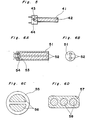
- Figs. 2A to 2E show longitudinal cross sections of one embodiment of the optical element integrated optical waveguide according to the present invention each of which comprises an optical waveguide part, a supporting member and a light emitting element.
- Fig. 2F is a transverse cross section of the optical waveguide of Fig. 2A.
- the optical waveguide part 12a is cylindrical and covered with the supporting member 11a, and its transverse cross sectional form does not change near the light emitting element 13a (see Fig. 2F).
- the optical waveguide part 12b expands near the light emitting element 13b and is covered with the supporting member 11b.
- the transverse cross section of the optical waveguide part is not necessarily round and can be ellipsoidal, star-like, triangle or square. Further, as shown in Fig. 2C, the size of the optical waveguide part 12c may gradually change.
- the optical waveguide part 12c is covered with the supporting member 11c and has the largest cross sectional area near the light emitting element 13c.
- the light emitting element 13d contacts the optical waveguide part 12d and is supported by the supporting member 11d.
- the light emitting element is not necessarily completely inserted into the supporting member.
- at least a part of the light emitting element 13e can be present in the optical waveguide part 12e which are covered with the supporting member 11e insofar as the light emitting member 13e is firmly fixed in the optical waveguide part 12e.
- the optical waveguides of Figs. 2A to 2E have comparative short length, they can be used in the same way as the commercially available LED which is embedded in the epoxy resin.
- Fig. 3 is a transverse cross section of one embodiment of the optical element integrated optical waveguide according to the present invention having an intermediate layer 23 between the the supporting member 21 and optical waveguide part 22.
- the refractive index of the intermediate layer 23 is lower than that of the optical waveguide part 22. Since the refractive index of the supporting member 21 is not necessarily lower than that of the optical waveguide part 22, the polymer of the supporting member 21 can be selected from wide variety of the materials.
- the intermediate layer 23 may be formed together with the production of the supporting member, for example, by co-extrusion of the supporting member and the intermediate layer. Alternatively, the intermediate layer may be formed by applying the material of the layer on the inner surface of the bore formed in the supporting member.
- Fig. 4A shows a longitudinal cross section of one embodiment of the optical element integrated optical waveguide according to the present invention having an optical waveguide part a part of which comprises an uncross-linked siloxane polymer.
- the refractive index of the supporting member 31 is lower than that of the part of the optical waveguide part 32 made of the liquid siloxane polymer.
- the hatched parts in Fig. 4A indicate the cured parts of the siloxane polymer, and the optical element 33 is embedded in either of the cured parts.
- the optical element 33 is firmly fixed in the optical waveguide so that handling property at the end of the optical waveguide is improved. Since the cured parts of the siloxane polymer are present at the both ends of the optical waveguide, the liquid siloxane polymer does not leak from the optical waveguide.
- the siloxane polymer to be filled in the bore of the supporting member should contain impurities in amounts as small as possible to minimize any factor that worsens the light transmission loss
- the siloxane polymer in the end regions may be cross linked with a cross linking agent and/or a cross linking aid according to the embodiment of Fig. 4A That is, the liquid siloxane polymer containing substantially no impurities is filled in a polymer tube and then the liquid siloxane polymer containing the cross linking agent and the like added not to disturb the interface between two layers of the liquid siloxane polymers. Then the optical elements is inserted in the liquid siloxane polymer followed by cross linking of the siloxane polymer in the end region.
- Fig. 4B shows a longitudinal cross section near the end of the optical waveguide where the optical element is embedded.
- the optical element is not necessarily embedded in the cured siloxane polymer.
- the outermost end region 34 of the optical waveguide part should consists of the cured siloxane polymer.
- the cured siloxane polymer fixes the bonding wires 38 and in turn the optical element 37 and prevents the leakage of the uncured liquid siloxane polymer.
- the siloxane polymer is the outermost end part 34 can be cross linked by any conventional method used for cross linking the siloxane polymer such as by irradiation and by means of the cross linking agent and/or the cross linking aid.
- the siloxane polymer 35 surrounding the optical element may be cured or not cured.
- the siloxane polymer 35 is preferably cross linked with the cross linking agent and/or the cross linking aid, particularly with a catalyst such as a platinum catalyst. Irradiation of the siloxane polymer 35 is not preferred since it deteriorates the optical element.
- the inner region 36 of the optical waveguide part may be in the liquid, elastic or solid state. When it is to be in the solid state, it can be cross linked by any conventional method as described in the above.
- the siloxane polymer may be in the liquid state or in the solid state.
- Fig. 5 shows a longitudinal cross section of one embodiment of the optical element integrated optical waveguide according to the present invention having a casing 44 to which the optical element 43 is connected to improve the connection of the optical element to an outer electric system.
- the optical waveguide part 42 has substantially the same structure as that of Fig. 2D, and a part of the optical element 43 is inserted in the supporting member 41.
- Figs. 6A and 6B show longitudinal and transverse cross sections of one embodiment of the optical element integrated optical waveguide according to the present inven tion which comprises two optical waveguide parts 52 in one supporting member 51. Since the optical waveguide parts 52 contain the light emitting element 53 and the light receiving element 54, respectively, this embodiment of the optical waveguide is suitable as a detecting sensor.
- the transverse cross sections of the optical waveguide parts are round in Fig. 6B, they may have other cross sectional forms.
- the cross sections of the two optical waveguide parts 57 surrounded by the supporting member 55 can be semicircle. Further, the cross section of the optical waveguide part may be square.
- optical element integrated optical waveguide as shown in Fig. 6D, three (or more) optical waveguide parts 58 are contained in the supporting member 57.
- the cross sectional form of the optical waveguide, and the cross sectional form and the number of the optical waveguide part are not critical in the present invention.
- the optical waveguide part is not necessarily straight and may be helical or other form. When two or more optical waveguide parts are contained in the supporting member, at least one of them should have the optical element but the rest of them need not.
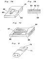
- Figs. 7A and 7B show a partly removed perspective view and a longitudinal cross section, respectively of an embodiment of the optical element integrated optical waveguide of the present invention, in which the optical element 63 placed on a substrate 64 is covered with the optical waveguide part 62 which is covered with a protective layer 61.
- the protective layer 61 provides the supporting member.
- the substrate 64 is made of any material which can reflect light such as a semiconductor substrate, a metal plate and mirror.
- the substrate is made of a plastic material.
- the optical element may be formed b growing a suitable material directly on the substrate.
- Fig. 7C shows a perspective view of another embodiment of the optical element integrated optical waveguide in which the optical element placed on the substrate is covered with the optical waveguide part.
- the optical waveguide part 67 formed on the substrate 69 is branched into three lines, each of which has one light emitting element 68 at its end.
- the optical waveguide part 67 is covered with the protective layer 66.
- Fig. 8 shows a perspective view of one embodiment of the optical element integrated optical waveguide according to the present invention in which the optical waveguide part 72 is covered with the supporting member 71 and branched into two lines at one end, each of which lines has the light emitting element (not shown).
- optical element is not shown in figures for simplicity.
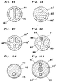
- Figs. 9A to 9C show transverse cross sections of embodiments of the optical element integrated optical waveguide according to the present invention which have at least one vacant bore in the supporting member.
- the optical waveguides of Figs. 9A and 9B have one optical waveguide part 82 or 82 ⁇ in the polymeric supporting member 81 or 82 ⁇ and one vacant bore 83 or 83 ⁇ . These bores in the optical waveguides of Figs. 9A and 9B have different cross sectional forms.
- the optical waveguide of Fig. 9C has two optical waveguide parts 82 ⁇ and two vacant bores 82 ⁇ . These optical waveguides of Figs.
- 9A to 9C can be produced by pouring the liquid siloxane polymer in at least one of the bores in the supporting member and cross linking it with leaving the rest of the bores vacant.
- the numbers of the optical waveguide part and/or the vacant bores are not critical and not limited to these embodiments.
- the vacant bore can be used for various purposes.
- a liquid or a gas is passed through it and an image fiber is inserted into it.
- an electrical wire or cable or a wire may be inserted in the vacant bore.
- Fig. 9D shows a transverse cross section of one embodiment of the optical element integrated optical waveguide according to the present invention which is used as a catheter with a balloon inserted in a blood vessel.
- This catheter can be used for inspecting the interior of the blood vesse.
- the optical waveguide part 85 in the supporting member 84 is used as a light guide for transmitting illumination light and the light emitting element (not shown) is used as an illuminant.
- An image fiber 89 is inserted into one of three vacant bores and other two bores 87 and 88 are used for inflating the balloon and for flushing, respectively.
- the balloon is inflated by supplying a suitable liquid through the bore 87 to fix the catheter in the blood vessel.
- a quantity of blood in the blood vessel is removed by flushing a suitable liquid such as a physiological saline from the bore 88.
- the interior of the blood vessel from which the blood is removed is inspected by means of the image fiber 89 with illuminating the interior by light transmitted through the light guide 88.
- Fig. 10A shows a transverse cross section of one embodiment of the optical element integrated optical waveguide according to the present invention having a tube like member.
- the optical waveguide comprises the supporting member 91, the optical waveguide part 92 and a tube like member 93 embedded in the optical waveguide part 92.
- a rod like member may be embedded.
- both the tube like member and the rod like member can be contained in the optical waveguide part.
- the numbers of the tube like member and/or the rod like member are not critical.
- the tube 93 is firstly fixed in the supporting member 91 by attaching them to a suitable positioning means with applying slight tension to them. Then, the liquid siloxane polymer is poured between the supporting member 91 and the tube 93 with keeping them vertical. After the optical element is positioned, the siloxane polymer is cross linked to form the optical waveguide part.
- Fig. 10B shows a transverse cross section of one embodiment of the optical element integrated optical waveguide, which comprises the supporting member 91 ⁇ , the optical waveguide part 92 ⁇ , an image fiber 95 ⁇ and two tube like members 93 ⁇ ,94 ⁇ .
- This optical waveguide is also used as a catheter.
- One of the tube like member serves for supplying a physiological saline to the balloon and the other serves removing air or the physiological saline from the balloon.
- Figs. 11A, 11B and 11C show transverse cross sections of three embodiments of the optical element integrated optical waveguide according to the present invention which contain the tube like member and/or the rod like member in the wall of the supporting member.
- the optical waveguide of Fig. 11A comprises the supporting member 101, the optical waveguide part 102 and two rod like members 103 such as electrical wires
- that of Fig. 11B comprises the supporting member 101 ⁇ , the optical waveguide part 102 ⁇ , the rod like member 103 ⁇ and the tube like member 104 ⁇
- that of Fig. 11C comprises the supporting member 101 ⁇ , two optical waveguide parts 102 ⁇ , two rod like member 103 ⁇ and two tube like member 104 ⁇ .
- the tube like member and the rod like member are embedded in the wall of the supporting member.
- These optical waveguides can be produced by extruding the supporting member together with the rod like member and/or the tube like member, pouring the liquid siloxane polymer in the bore(s) and then cross linking the siloxane polymer.
- the present invention includes embodiments in which the optical element integrated optical waveguides of Figs. 10 and 11 are combined. That is, in such optical waveguide, the tube like members and/or the rod like members are embedded in the optical waveguide part and the wall of the supporting member.
- Figs. 12A and 12B show transverse cross sections of one embodiment of the optical element integrated optical waveguide according to the present invention in which a part of the optical waveguide part, for example, along all the length of the optical waveguide part except the solidified end regions is in the liquid and gel states.
- the optical waveguide part comprises a liquid portion 112 or 112 ⁇ surrounded by a gel like portion 113 or 113 ⁇ encircled by broken line.
- the cross sectional forms of the liquid portions are different.
- the optical waveguide of Fig. 12B may be produced by irradiating the supporting member containing the liquid siloxane polymer from opposite two directions so as not to cross link the siloxane polymer in the liquid portion 113 ⁇ having an ellipsoidal cross section.
- the cross sectional area of the portion 113 or 113 ⁇ can be adjusted by, for example, controlling accelerating voltage of electron beam.
- the innermost portion may be in the gel state and the outer portion may be in the liquid state.
- the optical waveguide according to the present invention is used as a medical catheter, a light wave composer, an optical waveguide for an optical IC, a sensor and a light guide and further for optical communication. In addition, it can be used for LED and a semiconductor laser.
- a tube made of a tetrafluoroethylene/hexafluoropropylene copolymer (hereinafter referred to as "FEP") of 6 mm in inner diameter, 8 mm in outer diameter and 5 m in length which had been washed with a dust-free solvent, liquid polydimethylsiloxane having a weight average molecular weight of 1.5 x 10⁵ which had been filtered through a 2 ⁇ m filter was filled. Then, a bare red light LED (660 nm) (manufactured by Hikaridenshi Industries) was inserted from one end of the FEP tube. After wrapping a part of the FEP tube near the LED with a sheet of lead foil, electron beam was irradiated along the entire length of the FEP tube at a dose of 7 Mrad to cross link liquid polydimethylsiloxane.
- FEP tetrafluoroethylene/hexafluoropropylene copolymer
- liquid polydimethylsiloxane having a weight average molecular weight of 1.5 x 10⁵ which had been filtered through a 2 ⁇ m filter was filled, and a light LED (660 nm) covered with an epoxy resin layer (manufactured by Hikaridenshi Industries) was inserted from one end of the FEP tube.
- a light LED 660 nm
- an epoxy resin layer manufactured by Hikaridenshi Industries
- electron beam was irradiated along the entire length of the FEP tube at a dose of 3 Mrad to change liquid polydimethylsiloxane into the gel state. Thereafter, each end region of 20 cm was further irradiated at a dose of 4 Mrad to solidify polydimethylsiloxane in the end regions.
- liquid polydimethylsiloxane having a weight average molecular weight of 1.5 x 10⁵ was filled and both ends of the tube was sealed with glass rods.
- the entire length of the FEP tube was irradiated by electron beam at a dose of 7 Mrad to solidify polydimethylsiloxane, and then the glass rods were removed.
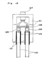
- the FEP tube containing solidified polydimethylsiloxane was cut into halves 120 and inserted in the bottom half of a black plastic case 121 through taps 122 as shown in Fig. 12.
- addition cross linking type polysiloxane 123 was poured and then a red LED 124 (manufactured by Hikaridenshi Industries) and a photodiode 125 (manufactured by Hamamatsu Photonics) were inserted therein, respectively. Over the LED and the photodiode, an epoxy resin 126 was poured. Finally, the each terminal was connected to a pin connector 127 attached to the upper half of the case 121 to complete the optical element integrated optical waveguide. When the LED was energized and the both end of the FEP tubes 120 was faced with a distance of several centimeters, the emitted red light was detected by the photodiode.
Landscapes
- Physics & Mathematics (AREA)
- General Physics & Mathematics (AREA)
- Optics & Photonics (AREA)
- Engineering & Computer Science (AREA)
- Mechanical Engineering (AREA)
- Microelectronics & Electronic Packaging (AREA)
- Optical Integrated Circuits (AREA)
- Optical Couplings Of Light Guides (AREA)
- Optical Fibers, Optical Fiber Cores, And Optical Fiber Bundles (AREA)
Applications Claiming Priority (2)
| Application Number | Priority Date | Filing Date | Title |
|---|---|---|---|
| JP19129/86 | 1986-01-29 | ||
| JP61019129A JPS6289914A (ja) | 1985-05-31 | 1986-01-29 | 光素子一体型光導波路およびその製法 |
Publications (3)
| Publication Number | Publication Date |
|---|---|
| EP0230520A2 true EP0230520A2 (fr) | 1987-08-05 |
| EP0230520A3 EP0230520A3 (en) | 1989-08-09 |
| EP0230520B1 EP0230520B1 (fr) | 1993-08-04 |
Family
ID=11990851
Family Applications (1)
| Application Number | Title | Priority Date | Filing Date |
|---|---|---|---|
| EP86114271A Expired - Lifetime EP0230520B1 (fr) | 1986-01-29 | 1986-10-15 | Guide d'onde optique à élément optique intégré et son procédé de fabrication |
Country Status (5)
| Country | Link |
|---|---|
| US (1) | US4762381A (fr) |
| EP (1) | EP0230520B1 (fr) |
| JP (1) | JPS6289914A (fr) |
| CA (1) | CA1270395A (fr) |
| DE (1) | DE3688835T2 (fr) |
Cited By (6)
| Publication number | Priority date | Publication date | Assignee | Title |
|---|---|---|---|---|
| EP0304939A3 (en) * | 1987-08-28 | 1990-10-10 | Hitachi, Ltd. | Optical part including integral combination of optical fiber and light emitting or receiving element and method of manufacturing the same |
| EP0481440A3 (en) * | 1990-10-19 | 1992-11-19 | Iot Entwicklungsgesellschaft Fuer Integrierte Optik-Technologie Mbh | Sensor for the detection of a substance |
| EP0617303A1 (fr) * | 1993-03-19 | 1994-09-28 | Akzo Nobel N.V. | Procédé d'intégration d'un composant semi-conducteur avec un composant guide d'onde optique polymère, et dispositif électro-optique avec une structure intégrée ainsi obtenu |
| EP0340557B1 (fr) * | 1988-04-28 | 1996-07-10 | Hoechst Aktiengesellschaft | Guide de lumière |
| WO2010105242A2 (fr) | 2009-03-12 | 2010-09-16 | Applied Precision, Inc. | Source de lumière à base de fibre optique |
| EP2610275A1 (fr) * | 2011-12-26 | 2013-07-03 | Nitto Denko Corporation | Composition de résine pour former un guide d'onde optique et guide d'onde optique utilisant la composition |
Families Citing this family (43)
| Publication number | Priority date | Publication date | Assignee | Title |
|---|---|---|---|---|
| GB2199210B (en) * | 1986-12-24 | 1991-02-13 | Motorola Israel Ltd | Optical coupling arrangements |
| DE59106807D1 (de) * | 1990-02-17 | 1995-12-07 | Stribel Gmbh | Signalübertragungsleitung. |
| JPH079441B2 (ja) * | 1991-03-20 | 1995-02-01 | 日本碍子株式会社 | 光応用センサおよびその製造方法 |
| US5305407A (en) * | 1992-10-06 | 1994-04-19 | The Walt Disney Company | Apparatus and method for underwater fiber-optic coupling |
| JP3087676B2 (ja) * | 1997-02-13 | 2000-09-11 | 日本電気株式会社 | ゲル状樹脂を用いた光結合系及び実装構造 |
| US6611635B1 (en) | 1998-10-09 | 2003-08-26 | Fujitsu Limited | Opto-electronic substrates with electrical and optical interconnections and methods for making |
| US6690845B1 (en) | 1998-10-09 | 2004-02-10 | Fujitsu Limited | Three-dimensional opto-electronic modules with electrical and optical interconnections and methods for making |
| US6684007B2 (en) | 1998-10-09 | 2004-01-27 | Fujitsu Limited | Optical coupling structures and the fabrication processes |
| US6785447B2 (en) | 1998-10-09 | 2004-08-31 | Fujitsu Limited | Single and multilayer waveguides and fabrication process |
| US6845184B1 (en) | 1998-10-09 | 2005-01-18 | Fujitsu Limited | Multi-layer opto-electronic substrates with electrical and optical interconnections and methods for making |
| US6706546B2 (en) | 1998-10-09 | 2004-03-16 | Fujitsu Limited | Optical reflective structures and method for making |
| US6343171B1 (en) | 1998-10-09 | 2002-01-29 | Fujitsu Limited | Systems based on opto-electronic substrates with electrical and optical interconnections and methods for making |
| JP2001074987A (ja) * | 1999-09-08 | 2001-03-23 | Yazaki Corp | レセプタクルの製造方法、レセプタクル、及び光コネクタ |
| JP2001274528A (ja) | 2000-01-21 | 2001-10-05 | Fujitsu Ltd | 薄膜デバイスの基板間転写方法 |
| US20030152309A1 (en) * | 2002-02-14 | 2003-08-14 | Howard James Robert | Printed circuit board containing optical elements |
| FR2840388B1 (fr) * | 2002-05-31 | 2004-07-30 | Valeo Vision | Feu de signalisation comportant une piece optique realisant une fonction de signalisation de maniere autonome |
| US20040186352A1 (en) * | 2003-03-20 | 2004-09-23 | Welch Allyn, Inc. | Illumination system for medical diagnostic instrument |
| US20050007346A1 (en) * | 2003-07-11 | 2005-01-13 | Guolin Ma | Optical conduit for channeling light onto a surface |
| US20080085122A1 (en) * | 2003-11-10 | 2008-04-10 | Melexis Nv | Optical Data Transmission, Optical Data Transceivers And Method Of Manufacturing And Packaging Thereof |
| AT413891B (de) * | 2003-12-29 | 2006-07-15 | Austria Tech & System Tech | Leiterplattenelement mit wenigstens einem licht-wellenleiter sowie verfahren zur herstellung eines solchen leiterplattenelements |
| US7570846B2 (en) * | 2004-06-21 | 2009-08-04 | Oree, Advanced Illumination Solutions Inc. | High efficacy waveguide coupler |
| JP4679198B2 (ja) * | 2004-08-23 | 2011-04-27 | オリンパスメディカルシステムズ株式会社 | 内視鏡 |
| US8128272B2 (en) | 2005-06-07 | 2012-03-06 | Oree, Inc. | Illumination apparatus |
| US8272758B2 (en) | 2005-06-07 | 2012-09-25 | Oree, Inc. | Illumination apparatus and methods of forming the same |
| US8215815B2 (en) | 2005-06-07 | 2012-07-10 | Oree, Inc. | Illumination apparatus and methods of forming the same |
| DE102005052356A1 (de) * | 2005-09-30 | 2007-04-12 | Osram Opto Semiconductors Gmbh | Beleuchtungseinheit mit Lumineszenzdiodenchip und Lichtleiter, Verfahren zum Herstellen einer Beleuchtungseinheit und LCD-Display |
| US20090001397A1 (en) * | 2007-05-29 | 2009-01-01 | Oree, Advanced Illumiation Solutions Inc. | Method and device for providing circumferential illumination |
| US8550684B2 (en) | 2007-12-19 | 2013-10-08 | Oree, Inc. | Waveguide-based packaging structures and methods for discrete lighting elements |
| US7929816B2 (en) | 2007-12-19 | 2011-04-19 | Oree, Inc. | Waveguide sheet containing in-coupling, propagation, and out-coupling regions |
| US8231237B2 (en) | 2008-03-05 | 2012-07-31 | Oree, Inc. | Sub-assembly and methods for forming the same |
| US8301002B2 (en) | 2008-07-10 | 2012-10-30 | Oree, Inc. | Slim waveguide coupling apparatus and method |
| US8297786B2 (en) | 2008-07-10 | 2012-10-30 | Oree, Inc. | Slim waveguide coupling apparatus and method |
| US8624527B1 (en) | 2009-03-27 | 2014-01-07 | Oree, Inc. | Independently controllable illumination device |
| US20100320904A1 (en) | 2009-05-13 | 2010-12-23 | Oree Inc. | LED-Based Replacement Lamps for Incandescent Fixtures |
| WO2010150202A2 (fr) | 2009-06-24 | 2010-12-29 | Oree, Advanced Illumination Solutions Inc. | Appareil d'éclairage à efficacité de conversion élevée et procédés de formation associés |
| JP5959505B2 (ja) * | 2011-03-28 | 2016-08-02 | 古河電気工業株式会社 | 光導波路回路 |
| JP2013057809A (ja) * | 2011-09-08 | 2013-03-28 | Murata Mfg Co Ltd | 光ファイバ、光ファイバモジュール及び光ファイバの製造方法 |
| JP2013057876A (ja) * | 2011-09-09 | 2013-03-28 | Murata Mfg Co Ltd | ケーブルモジュール |
| US8591072B2 (en) | 2011-11-16 | 2013-11-26 | Oree, Inc. | Illumination apparatus confining light by total internal reflection and methods of forming the same |
| WO2014006501A1 (fr) | 2012-07-03 | 2014-01-09 | Yosi Shani | Appareil d'éclairage au phosphore distant planaire |
| US10353146B2 (en) * | 2017-06-28 | 2019-07-16 | Intel Corporation | Flexible and stretchable optical interconnect in wearable systems |
| GB201813343D0 (en) | 2018-08-15 | 2018-09-26 | Univ Manchester | Electrically controlled active wave guides |
| WO2022076894A1 (fr) | 2020-10-08 | 2022-04-14 | Avicenatech Corp. | Intégration de dispositifs oe avec des circuits intégrés |
Family Cites Families (10)
| Publication number | Priority date | Publication date | Assignee | Title |
|---|---|---|---|---|
| GB897696A (en) * | 1957-11-08 | 1962-05-30 | Standard Telephones Cables Ltd | Flexible light guide |
| US4433898A (en) * | 1980-12-22 | 1984-02-28 | National Semiconductor Corporation | Fiber optic assembly for coupling an optical fiber and a light source |
| JPS592005A (ja) * | 1982-06-26 | 1984-01-07 | Sumitomo Electric Ind Ltd | センサ用光フアイバ |
| US4557550A (en) * | 1982-10-27 | 1985-12-10 | Raychem Corporation | Optical fiber taps |
| JPS59154407A (ja) * | 1983-02-22 | 1984-09-03 | Sumitomo Electric Ind Ltd | イメ−ジフアイバ |
| US4547040A (en) * | 1983-06-21 | 1985-10-15 | Mitsubishi Rayon Co., Ltd. | Optical fiber assembly and process for preparing same |
| DE3479160D1 (en) * | 1983-08-18 | 1989-08-31 | Mitsubishi Rayon Co | Optical transmission fibers and process for their production |
| US4535141A (en) * | 1984-03-23 | 1985-08-13 | Dow Corning Corporation | Liquid curable polyorganosiloxane compositions |
| EP0173266A3 (fr) * | 1984-08-24 | 1987-09-16 | Sumitomo Electric Industries Limited | Guide d'ondes optiques composé et sa fabrication |
| JPS6159303A (ja) * | 1984-08-30 | 1986-03-26 | Mitsubishi Rayon Co Ltd | プラスチツク系光学繊維 |
-
1986
- 1986-01-29 JP JP61019129A patent/JPS6289914A/ja active Pending
- 1986-10-15 EP EP86114271A patent/EP0230520B1/fr not_active Expired - Lifetime
- 1986-10-15 DE DE86114271T patent/DE3688835T2/de not_active Expired - Fee Related
- 1986-10-17 CA CA000520717A patent/CA1270395A/fr not_active Expired - Lifetime
- 1986-11-03 US US06/926,176 patent/US4762381A/en not_active Expired - Fee Related
Cited By (10)
| Publication number | Priority date | Publication date | Assignee | Title |
|---|---|---|---|---|
| EP0304939A3 (en) * | 1987-08-28 | 1990-10-10 | Hitachi, Ltd. | Optical part including integral combination of optical fiber and light emitting or receiving element and method of manufacturing the same |
| EP0340557B1 (fr) * | 1988-04-28 | 1996-07-10 | Hoechst Aktiengesellschaft | Guide de lumière |
| EP0481440A3 (en) * | 1990-10-19 | 1992-11-19 | Iot Entwicklungsgesellschaft Fuer Integrierte Optik-Technologie Mbh | Sensor for the detection of a substance |
| US5262842A (en) * | 1990-10-19 | 1993-11-16 | IOT Entwicklungsgesellschaft fur integrierte Optiktechnologie mbH | Optical sensor having a wave guide substrate with interferometer integrated therein |
| EP0617303A1 (fr) * | 1993-03-19 | 1994-09-28 | Akzo Nobel N.V. | Procédé d'intégration d'un composant semi-conducteur avec un composant guide d'onde optique polymère, et dispositif électro-optique avec une structure intégrée ainsi obtenu |
| US5764820A (en) * | 1993-03-19 | 1998-06-09 | Akzo Nobel Nv | Method of forming integrated electro-optical device containing polymeric waveguide and semiconductor |
| WO2010105242A2 (fr) | 2009-03-12 | 2010-09-16 | Applied Precision, Inc. | Source de lumière à base de fibre optique |
| EP2406676A4 (fr) * | 2009-03-12 | 2017-10-11 | GE Healthcare Bio-Sciences Corp. | Source de lumière à base de fibre optique |
| EP2610275A1 (fr) * | 2011-12-26 | 2013-07-03 | Nitto Denko Corporation | Composition de résine pour former un guide d'onde optique et guide d'onde optique utilisant la composition |
| US9034566B2 (en) | 2011-12-26 | 2015-05-19 | Nitto Denko Corporation | Resin composition for forming optical waveguide and optical waveguide using the composition |
Also Published As
| Publication number | Publication date |
|---|---|
| JPS6289914A (ja) | 1987-04-24 |
| EP0230520A3 (en) | 1989-08-09 |
| EP0230520B1 (fr) | 1993-08-04 |
| US4762381A (en) | 1988-08-09 |
| DE3688835T2 (de) | 1993-12-09 |
| DE3688835D1 (de) | 1993-09-09 |
| CA1270395A (fr) | 1990-06-19 |
Similar Documents
| Publication | Publication Date | Title |
|---|---|---|
| EP0230520B1 (fr) | Guide d'onde optique à élément optique intégré et son procédé de fabrication | |
| EP0097934B1 (fr) | Cathéter transmetteur d'images à fibres optiques composées et procédé de fabrication | |
| EP3539451B1 (fr) | Partie de pointe pour dispositif de vision insérable | |
| US5615293A (en) | Fiber optic cable assembly for facilitating the installation thereof in a structure | |
| US4957347A (en) | Clad optical conduit and method of manufacture | |
| US3641332A (en) | Fiber optics illumination system | |
| US20210068642A1 (en) | Tip part assembly for an endoscope | |
| US7570852B2 (en) | Optical fiber cable suited for blown installation or pushing installation in microducts of small diameter | |
| EP0157610B1 (fr) | Gainage pour fibres optiques | |
| US20090087153A1 (en) | Optical Fiber Microcable with Multilayer Protective Sheath | |
| JPH02155122A (ja) | 通信ケーブル | |
| US5149467A (en) | Improved method of manufacture for clad optical conduit | |
| EP0215173A1 (fr) | Cathéter à résistance optimale contre le courbage et méthode de fabrication | |
| EP0833174A2 (fr) | Système de transmission de lumière avec bifurcation à guide d'ondes optiques | |
| EP0173266A2 (fr) | Guide d'ondes optiques composé et sa fabrication | |
| EP0764863A1 (fr) | Câble de fibres optiques modulaire | |
| JPS62175703A (ja) | 有機シロキサン光導波路およびその製法 | |
| JP3974112B2 (ja) | 光伝送体、光伝送体と光学デバイスの接続部構造と、光伝送体の製造方法 | |
| JP2002055246A (ja) | 耐熱プラスチック光ファイバユニット | |
| EP0229202A1 (fr) | Guide d'ondes optique et son procédé de fabrication | |
| JPS6155609A (ja) | 複合光導波路 | |
| EP0987488A1 (fr) | Appareil d'éclairage optique | |
| JPH07192518A (ja) | トンネル | |
| JPH06174930A (ja) | 太陽光導光装置 | |
| JPH10300557A (ja) | 液面センサ |
Legal Events
| Date | Code | Title | Description |
|---|---|---|---|
| PUAI | Public reference made under article 153(3) epc to a published international application that has entered the european phase |
Free format text: ORIGINAL CODE: 0009012 |
|
| AK | Designated contracting states |
Kind code of ref document: A2 Designated state(s): DE FR GB |
|
| PUAL | Search report despatched |
Free format text: ORIGINAL CODE: 0009013 |
|
| AK | Designated contracting states |
Kind code of ref document: A3 Designated state(s): DE FR GB |
|
| 16A | New documents despatched to applicant after publication of the search report | ||
| 17P | Request for examination filed |
Effective date: 19890915 |
|
| RAP1 | Party data changed (applicant data changed or rights of an application transferred) |
Owner name: SUMITOMO ELECTRIC INDUSTRIES, LIMITED |
|
| RIN1 | Information on inventor provided before grant (corrected) |
Inventor name: OSAWA, YOSHITAKA C/O OSAKA WORKS OF Inventor name: NIWA, SHIN-ICHIRO C/O OSAKA WORKS OF Inventor name: NISHIMURA, AKIRA C/O OSAKA WORKS OF Inventor name: SHIBATA, YUTAKA C/O OSAKA WORKS OF Inventor name: UEMIYA, TAKAFUMI C/O OSAKA WORKS OF |
|
| 17Q | First examination report despatched |
Effective date: 19910805 |
|
| GRAA | (expected) grant |
Free format text: ORIGINAL CODE: 0009210 |
|
| AK | Designated contracting states |
Kind code of ref document: B1 Designated state(s): DE FR GB |
|
| REF | Corresponds to: |
Ref document number: 3688835 Country of ref document: DE Date of ref document: 19930909 |
|
| ET | Fr: translation filed | ||
| REG | Reference to a national code |
Ref country code: GB Ref legal event code: 746 Effective date: 19931221 |
|
| REG | Reference to a national code |
Ref country code: FR Ref legal event code: DL |
|
| PLBE | No opposition filed within time limit |
Free format text: ORIGINAL CODE: 0009261 |
|
| STAA | Information on the status of an ep patent application or granted ep patent |
Free format text: STATUS: NO OPPOSITION FILED WITHIN TIME LIMIT |
|
| 26N | No opposition filed | ||
| PGFP | Annual fee paid to national office [announced via postgrant information from national office to epo] |
Ref country code: GB Payment date: 19941005 Year of fee payment: 9 |
|
| PGFP | Annual fee paid to national office [announced via postgrant information from national office to epo] |
Ref country code: DE Payment date: 19941010 Year of fee payment: 9 |
|
| PGFP | Annual fee paid to national office [announced via postgrant information from national office to epo] |
Ref country code: FR Payment date: 19941011 Year of fee payment: 9 |
|
| PG25 | Lapsed in a contracting state [announced via postgrant information from national office to epo] |
Ref country code: GB Effective date: 19951015 |
|
| GBPC | Gb: european patent ceased through non-payment of renewal fee |
Effective date: 19951015 |
|
| PG25 | Lapsed in a contracting state [announced via postgrant information from national office to epo] |
Ref country code: FR Effective date: 19960628 |
|
| PG25 | Lapsed in a contracting state [announced via postgrant information from national office to epo] |
Ref country code: DE Effective date: 19960702 |
|
| REG | Reference to a national code |
Ref country code: FR Ref legal event code: ST |