EP0230615A2 - Polyimide mit Silizium, verwendet als Stop für das Sauerstoff-Ätzen und als zusammengesetzte dielektrische Beschichtungen - Google Patents
Polyimide mit Silizium, verwendet als Stop für das Sauerstoff-Ätzen und als zusammengesetzte dielektrische Beschichtungen Download PDFInfo
- Publication number
- EP0230615A2 EP0230615A2 EP86117617A EP86117617A EP0230615A2 EP 0230615 A2 EP0230615 A2 EP 0230615A2 EP 86117617 A EP86117617 A EP 86117617A EP 86117617 A EP86117617 A EP 86117617A EP 0230615 A2 EP0230615 A2 EP 0230615A2
- Authority
- EP
- European Patent Office
- Prior art keywords
- layer
- silicon
- substrate
- lift
- containing polyimide
- Prior art date
- Legal status (The legal status is an assumption and is not a legal conclusion. Google has not performed a legal analysis and makes no representation as to the accuracy of the status listed.)
- Withdrawn
Links
Images

Classifications
-
- H—ELECTRICITY
- H10—SEMICONDUCTOR DEVICES; ELECTRIC SOLID-STATE DEVICES NOT OTHERWISE PROVIDED FOR
- H10P—GENERIC PROCESSES OR APPARATUS FOR THE MANUFACTURE OR TREATMENT OF DEVICES COVERED BY CLASS H10
- H10P14/00—Formation of materials, e.g. in the shape of layers or pillars
- H10P14/60—Formation of materials, e.g. in the shape of layers or pillars of insulating materials
- H10P14/69—Inorganic materials
- H10P14/692—Inorganic materials composed of oxides, glassy oxides or oxide-based glasses
- H10P14/6921—Inorganic materials composed of oxides, glassy oxides or oxide-based glasses containing silicon
- H10P14/6922—Inorganic materials composed of oxides, glassy oxides or oxide-based glasses containing silicon the material containing Si, O and at least one of H, N, C, F or other non-metal elements, e.g. SiOC, SiOC:H or SiONC
-
- G—PHYSICS
- G03—PHOTOGRAPHY; CINEMATOGRAPHY; ANALOGOUS TECHNIQUES USING WAVES OTHER THAN OPTICAL WAVES; ELECTROGRAPHY; HOLOGRAPHY
- G03F—PHOTOMECHANICAL PRODUCTION OF TEXTURED OR PATTERNED SURFACES, e.g. FOR PRINTING, FOR PROCESSING OF SEMICONDUCTOR DEVICES; MATERIALS THEREFOR; ORIGINALS THEREFOR; APPARATUS SPECIALLY ADAPTED THEREFOR
- G03F7/00—Photomechanical, e.g. photolithographic, production of textured or patterned surfaces, e.g. printing surfaces; Materials therefor, e.g. comprising photoresists; Apparatus specially adapted therefor
- G03F7/004—Photosensitive materials
- G03F7/075—Silicon-containing compounds
- G03F7/0757—Macromolecular compounds containing Si-O, Si-C or Si-N bonds
-
- G—PHYSICS
- G03—PHOTOGRAPHY; CINEMATOGRAPHY; ANALOGOUS TECHNIQUES USING WAVES OTHER THAN OPTICAL WAVES; ELECTROGRAPHY; HOLOGRAPHY
- G03F—PHOTOMECHANICAL PRODUCTION OF TEXTURED OR PATTERNED SURFACES, e.g. FOR PRINTING, FOR PROCESSING OF SEMICONDUCTOR DEVICES; MATERIALS THEREFOR; ORIGINALS THEREFOR; APPARATUS SPECIALLY ADAPTED THEREFOR
- G03F7/00—Photomechanical, e.g. photolithographic, production of textured or patterned surfaces, e.g. printing surfaces; Materials therefor, e.g. comprising photoresists; Apparatus specially adapted therefor
- G03F7/004—Photosensitive materials
- G03F7/09—Photosensitive materials characterised by structural details, e.g. supports, auxiliary layers
- G03F7/094—Multilayer resist systems, e.g. planarising layers
-
- H—ELECTRICITY
- H10—SEMICONDUCTOR DEVICES; ELECTRIC SOLID-STATE DEVICES NOT OTHERWISE PROVIDED FOR
- H10P—GENERIC PROCESSES OR APPARATUS FOR THE MANUFACTURE OR TREATMENT OF DEVICES COVERED BY CLASS H10
- H10P14/00—Formation of materials, e.g. in the shape of layers or pillars
- H10P14/60—Formation of materials, e.g. in the shape of layers or pillars of insulating materials
- H10P14/66—Formation of materials, e.g. in the shape of layers or pillars of insulating materials characterised by the type of materials
- H10P14/662—Laminate layers, e.g. stacks of alternating high-k metal oxides
-
- H—ELECTRICITY
- H10—SEMICONDUCTOR DEVICES; ELECTRIC SOLID-STATE DEVICES NOT OTHERWISE PROVIDED FOR
- H10P—GENERIC PROCESSES OR APPARATUS FOR THE MANUFACTURE OR TREATMENT OF DEVICES COVERED BY CLASS H10
- H10P50/00—Etching of wafers, substrates or parts of devices
- H10P50/20—Dry etching; Plasma etching; Reactive-ion etching
- H10P50/28—Dry etching; Plasma etching; Reactive-ion etching of insulating materials
- H10P50/286—Dry etching; Plasma etching; Reactive-ion etching of insulating materials of organic materials
- H10P50/287—Dry etching; Plasma etching; Reactive-ion etching of insulating materials of organic materials by chemical means
-
- H—ELECTRICITY
- H10—SEMICONDUCTOR DEVICES; ELECTRIC SOLID-STATE DEVICES NOT OTHERWISE PROVIDED FOR
- H10P—GENERIC PROCESSES OR APPARATUS FOR THE MANUFACTURE OR TREATMENT OF DEVICES COVERED BY CLASS H10
- H10P76/00—Manufacture or treatment of masks on semiconductor bodies, e.g. by lithography or photolithography
- H10P76/20—Manufacture or treatment of masks on semiconductor bodies, e.g. by lithography or photolithography of masks comprising organic materials
- H10P76/202—Manufacture or treatment of masks on semiconductor bodies, e.g. by lithography or photolithography of masks comprising organic materials for lift-off processes
-
- H—ELECTRICITY
- H10—SEMICONDUCTOR DEVICES; ELECTRIC SOLID-STATE DEVICES NOT OTHERWISE PROVIDED FOR
- H10W—GENERIC PACKAGES, INTERCONNECTIONS, CONNECTORS OR OTHER CONSTRUCTIONAL DETAILS OF DEVICES COVERED BY CLASS H10
- H10W20/00—Interconnections in chips, wafers or substrates
- H10W20/01—Manufacture or treatment
- H10W20/031—Manufacture or treatment of conductive parts of the interconnections
- H10W20/056—Manufacture or treatment of conductive parts of the interconnections by filling conductive material into holes, grooves or trenches
- H10W20/058—Manufacture or treatment of conductive parts of the interconnections by filling conductive material into holes, grooves or trenches by depositing on sacrificial masks, e.g. using lift-off
-
- H—ELECTRICITY
- H10—SEMICONDUCTOR DEVICES; ELECTRIC SOLID-STATE DEVICES NOT OTHERWISE PROVIDED FOR
- H10W—GENERIC PACKAGES, INTERCONNECTIONS, CONNECTORS OR OTHER CONSTRUCTIONAL DETAILS OF DEVICES COVERED BY CLASS H10
- H10W20/00—Interconnections in chips, wafers or substrates
- H10W20/01—Manufacture or treatment
- H10W20/031—Manufacture or treatment of conductive parts of the interconnections
- H10W20/063—Manufacture or treatment of conductive parts of the interconnections by forming conductive members before forming protective insulating material
-
- Y—GENERAL TAGGING OF NEW TECHNOLOGICAL DEVELOPMENTS; GENERAL TAGGING OF CROSS-SECTIONAL TECHNOLOGIES SPANNING OVER SEVERAL SECTIONS OF THE IPC; TECHNICAL SUBJECTS COVERED BY FORMER USPC CROSS-REFERENCE ART COLLECTIONS [XRACs] AND DIGESTS
- Y10—TECHNICAL SUBJECTS COVERED BY FORMER USPC
- Y10S—TECHNICAL SUBJECTS COVERED BY FORMER USPC CROSS-REFERENCE ART COLLECTIONS [XRACs] AND DIGESTS
- Y10S428/00—Stock material or miscellaneous articles
- Y10S428/901—Printed circuit
-
- Y—GENERAL TAGGING OF NEW TECHNOLOGICAL DEVELOPMENTS; GENERAL TAGGING OF CROSS-SECTIONAL TECHNOLOGIES SPANNING OVER SEVERAL SECTIONS OF THE IPC; TECHNICAL SUBJECTS COVERED BY FORMER USPC CROSS-REFERENCE ART COLLECTIONS [XRACs] AND DIGESTS
- Y10—TECHNICAL SUBJECTS COVERED BY FORMER USPC
- Y10S—TECHNICAL SUBJECTS COVERED BY FORMER USPC CROSS-REFERENCE ART COLLECTIONS [XRACs] AND DIGESTS
- Y10S438/00—Semiconductor device manufacturing: process
- Y10S438/942—Masking
- Y10S438/948—Radiation resist
- Y10S438/95—Multilayer mask including nonradiation sensitive layer
-
- Y—GENERAL TAGGING OF NEW TECHNOLOGICAL DEVELOPMENTS; GENERAL TAGGING OF CROSS-SECTIONAL TECHNOLOGIES SPANNING OVER SEVERAL SECTIONS OF THE IPC; TECHNICAL SUBJECTS COVERED BY FORMER USPC CROSS-REFERENCE ART COLLECTIONS [XRACs] AND DIGESTS
- Y10—TECHNICAL SUBJECTS COVERED BY FORMER USPC
- Y10S—TECHNICAL SUBJECTS COVERED BY FORMER USPC CROSS-REFERENCE ART COLLECTIONS [XRACs] AND DIGESTS
- Y10S438/00—Semiconductor device manufacturing: process
- Y10S438/97—Specified etch stop material
-
- Y—GENERAL TAGGING OF NEW TECHNOLOGICAL DEVELOPMENTS; GENERAL TAGGING OF CROSS-SECTIONAL TECHNOLOGIES SPANNING OVER SEVERAL SECTIONS OF THE IPC; TECHNICAL SUBJECTS COVERED BY FORMER USPC CROSS-REFERENCE ART COLLECTIONS [XRACs] AND DIGESTS
- Y10—TECHNICAL SUBJECTS COVERED BY FORMER USPC
- Y10T—TECHNICAL SUBJECTS COVERED BY FORMER US CLASSIFICATION
- Y10T29/00—Metal working
- Y10T29/49—Method of mechanical manufacture
- Y10T29/49002—Electrical device making
- Y10T29/49117—Conductor or circuit manufacturing
- Y10T29/49124—On flat or curved insulated base, e.g., printed circuit, etc.
- Y10T29/49155—Manufacturing circuit on or in base
-
- Y—GENERAL TAGGING OF NEW TECHNOLOGICAL DEVELOPMENTS; GENERAL TAGGING OF CROSS-SECTIONAL TECHNOLOGIES SPANNING OVER SEVERAL SECTIONS OF THE IPC; TECHNICAL SUBJECTS COVERED BY FORMER USPC CROSS-REFERENCE ART COLLECTIONS [XRACs] AND DIGESTS
- Y10—TECHNICAL SUBJECTS COVERED BY FORMER USPC
- Y10T—TECHNICAL SUBJECTS COVERED BY FORMER US CLASSIFICATION
- Y10T428/00—Stock material or miscellaneous articles
- Y10T428/12—All metal or with adjacent metals
- Y10T428/12389—All metal or with adjacent metals having variation in thickness
- Y10T428/12396—Discontinuous surface component
-
- Y—GENERAL TAGGING OF NEW TECHNOLOGICAL DEVELOPMENTS; GENERAL TAGGING OF CROSS-SECTIONAL TECHNOLOGIES SPANNING OVER SEVERAL SECTIONS OF THE IPC; TECHNICAL SUBJECTS COVERED BY FORMER USPC CROSS-REFERENCE ART COLLECTIONS [XRACs] AND DIGESTS
- Y10—TECHNICAL SUBJECTS COVERED BY FORMER USPC
- Y10T—TECHNICAL SUBJECTS COVERED BY FORMER US CLASSIFICATION
- Y10T428/00—Stock material or miscellaneous articles
- Y10T428/12—All metal or with adjacent metals
- Y10T428/12493—Composite; i.e., plural, adjacent, spatially distinct metal components [e.g., layers, joint, etc.]
- Y10T428/12528—Semiconductor component
-
- Y—GENERAL TAGGING OF NEW TECHNOLOGICAL DEVELOPMENTS; GENERAL TAGGING OF CROSS-SECTIONAL TECHNOLOGIES SPANNING OVER SEVERAL SECTIONS OF THE IPC; TECHNICAL SUBJECTS COVERED BY FORMER USPC CROSS-REFERENCE ART COLLECTIONS [XRACs] AND DIGESTS
- Y10—TECHNICAL SUBJECTS COVERED BY FORMER USPC
- Y10T—TECHNICAL SUBJECTS COVERED BY FORMER US CLASSIFICATION
- Y10T428/00—Stock material or miscellaneous articles
- Y10T428/31504—Composite [nonstructural laminate]
- Y10T428/31721—Of polyimide
Definitions
- This invention relates to the fabrication of semiconductor components such as integrated circuits.
- silicon-containing polyimides as an oxygen etch barrier in a metal lift-off process and as an oxygen etch stop in the fabrication of multi-layer metal structures is disclosed.
- the lift-off method for forming metallized structures generally involves the fabrication of a multi-layer stencil comprising a solvent removable polymer film as the base or lift-off layer on a substrate.
- This lift-off layer is sequentially overcoated with a thin oxygen reactive ion etch (RIE) barrier and a resist layer.
- RIE reactive ion etch
- the desired pattern in the resist is delineated by standard lithographic techniques and then replicated into the underlying barrier layer by the RIE process using CF4 ambient, followed by O2 to etch the pattern into the lift-off layer.
- Subsequent blanket metal evaporation and solvent soak e.g., N-methylpyrrolidone (NMP) is employed to accomplish the removal of the lift-off stencil, leaving the desired metal pattern intact.
- NMP N-methylpyrrolidone
- the conventional O2 RIE barrier films as employed in the prior art include SiO x , Si3N4, sputtered quartz, polydimethylsiloxane resins, and plasma-polymerized organosilicon films.
- the conventional barrier films have been employed effectively as masking layers for O2 RIE processes in multi-layer metal structures, there are several major drawbacks associated with the use of these materials as discussed below.
- inorganic films such as silicon oxide and silicon nitride.
- These high temperatures can be detrimental to underlying organic polymer films resulting in reticulation and shriveling, in addition to the formation of debris at the organic/inorganic film interface.
- inorganic thin films invariably show high defect density (pinholes) which render them unacceptable for the fine line lithography required in the fabrication of high density integrated circuits.
- Inorganic barrier films in contact with organic polymer films such as polyimide also have problems of process induced stress cracking of the entire structure due to the mismatch in the coefficients of thermal expansion and the residual stress levels in inorganic versus organic films.
- Plasma polymerized organosilicon films for use as O2 RIE resistant layers as described in U.S. Patent 4,493,855 are free from the problems of the other prior art previously mentioned.
- the solution coated barrier films of this invention provide an inexpensive alternative requiring no special tooling and are specially suited for high volume manufacturing.
- a further advantage of the barrier films of this invention is the superior adhesion to a variety of organic and inorganic contacting layers without requiring any special surface preparation.
- U.S. Patent 4,430,153 discloses the in-situ conversion of an alkyl polyamide/polyimide surface layer to a silicon-containing alkyl polyamide/polyimide layer. This process, however, is unsuitable for practical applications requiring metal lift-off structures due to interference of the processing solvents with the mechanical integrity of the solvent removable lift-off layers. Also, this treatment does not provide an effective O2 RIE resistance necessary for pattern transfer into the underlayer.
- Another object of this invention is to provide a simple alternative to the Si3N4, SiO x deposited by CVD or plasma-enhanced CVD processes, plasma polymerized organo- silicons such as HMDS (hexamethyldisilazane) or hexamethyldisiloxane used as oxygen etch stops and dual dielectric in the fabrication of multi-level metal structures.
- HMDS hexamethyldisilazane
- hexamethyldisiloxane used as oxygen etch stops
- dual dielectric in the fabrication of multi-level metal structures.
- the fabrication of multi-level metal structures is carried out according to the multi-layer resist process utilizing pre-formed silicon-containing polyimides as O2/RIE barriers and etch stops.
- the silicon-containing polyimides either spun-on or sprayed-on, have the requisite properties in terms of the thermal stability, glass transition temperature, mechanical properties, solvent resistance, compatibility of thermal coefficients of expansion with contacting films, and the necessary O2 etch resistance.
- Thin films of silicon-containing polyimide formulations utilized in this invention are pinhole free, provide the desired overhang after RIE into the underlying lift-off layer, show no outgassing or fencing during metallization, and allow for clean lift-off in the usual solvent soak to provide excellent metal pattern.
- the barrier films according to this invention exhibit excellent O2 RIE resistance, adhesion to commonly employed lift-off layers, resist films, inter-level dielectric layers such as polyimide, and inorganic layers such as silicon oxide, silicon nitride, etc.
- the silicon-containing polyimides as utilized in this invention, can remain as an integral part of the structure in packaging technology if desired.
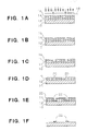
- a substrate 10 such as a silicon wafer having semiconductor devices, is surface treated with a 0.1 % aqueous solution of q-aminopropyltriethoxysilane (q-APS) by spin application at 2,000 RPM for 30 seconds, followed by a 5 minute bake at 85° C (hot plate).
- the surface treatment enhances the adhesion between the substrate 10 and a subsequently applied underlayer 12.
- the lift-off underlayer is spin applied at 2,000 RPM for 30 seconds and baked at 85° C for 10 minutes, 150° C for 15 minutes, and 230° C for 20 minutes, to form an approximately 2.1 micron thick coating.
- AZ1350J commercially available from the Shipley Company has been used advantageously as the lift-off layer.
- the lift-off layer is not critical so long as it can be etched with O2 plasma or RIE processing.
- This layer typically includes organic polymers such as AZ1350, AZ1350J (products of Shipley Co.), polysulfone resin (ICI Company), or soluble polyimides.
- Silicon-containing polyimide # 250-65 or # 250-50 available commercially from the M&T Company, is diluted 1:2.5 with diglyme, filtered through a 0.45 micron silver filter, and spin-applied on the baked lift-off layer 12 at 3,000 RPM for 30 seconds.
- a bake sequence of 85° C for 10 minutes, 150° C for 15 minutes, and 230° C for 20 minutes follows, resulting in an approximately 0.25-0.30 micron thick layer of the silicon polyimide.
- a layer of resist 16 is applied over the silicon-containing polyimide barrier layer 14.
- the surface of silicon-polyimide layer 14 is pre-treated with HMDS-qAPS vapor in Freon-TF for 5 minutes or with a 0.1 % solution of a q-APS in toluene by spin coating.
- the layer of diazonaphthoquinone-novolak resist 16 is applied at 3,000 RPM for 30 seconds followed by a 30 minute bake at 85° C to form a thick film approximately 0.9 - 1.1 microns thick.
- the resist layer 16 can be a standard resist material known in the art, it may be positive or negative, and may be sensitive to near, mid or deep UV; electron beam; X-ray; ion beam; or laser. Examples are novolak based resists with diazoquinone type of photoactive component, acrylate polymers such as PMMA, polyolefin sulfones, etc. Patterning of the resist can be carried out according to standard lithographic processes.
- resist layer 16 is developed with AZ2401 (Shipley Co.) developed diluted 1:3.5 with deionized water (Fig. 1B).
- the image in the resist layer 16 is subsequently replicated into the silicon-containing polyimide layer 14 by RIE using a CF4-O2 mixed gas system at a 2.5:1 flow rate ratio at 50.5 to 63.8 ⁇ bar, with power level in the range 250-300 watts. Under these conditions, the barrier layer 14 can be etched at the rate of 110 - 130 nm/min. The resulting structure is shown in Fig. 1C.
- the silicon-containing polyimide layer 14 and exposed areas of substrate 10 are sputter cleaned for 6 minutes at 220° C prior to metallization.
- a blanket layer of metal 22, such as Al-Cu, is evaporated over the exposed surfaces at 120° C to 150° C.
- the lift-off is accomplished by the standard solvent soak in NMP for 2 hours with brief ultrasonic agitation to accelerate removal of the lift-off stencil, leaving the metallurgy network 22 as shown in Fig. 1F.
- the metal film may be any metal conventionally employed, e.g., aluminum, copper alloy, palladium, platinum, chromium, etc.
- soluble polyimide XU284, manufactured by CIBA GEIGY, or other lift-off layers can be used in place of the baked AZ layer 12 without departing from the scope of this invention.
- the lift-off layer can be 1 - 5 ⁇ m in thickness
- the silicon polyimide layer is typically in the range 0.15 - 0.65 ⁇ m
- the imaging layer thickness is adjusted such that the desired level of image resolution and reduction of defect density is achieved.
- the imaging layer thickness is typically in the range 0.15 - 7.2 ⁇ m. All other processing steps would follow as described above.
- a substrate 30, which can be a semiconductor wafer or packaging substrate, is provided.
- a lift-off layer 32 which can be a photoresist material or other polymer, is next applied on the substrate 30 as previously described.
- a 10 % solution of silicon-polyimide BE221 (available from M&T Company) in NMP is doped with a diazonaphthoqui-none-based photoactive compound (PAC).
- PAC diazonaphthoqui-none-based photoactive compound
- the photoactive compound comprises approximately 18 % of the solution.
- the mixture is filtered through a 0.2 micron silver filter and spin applied on lift-off layer 32.
- the resulting silicon-polyimide/PAC layer 34 is exposed to mid-UV exposure through mask 36 for approximately 20 seconds.
- metal 38 is blanket deposited on the layer 34 and exposed areas of substrate 30 (Fig. 2D), resulting in the metallurgy pattern after removal of the lift-off stencil as seen in Fig. 2E.
- silicon-containing polyimides are useful as O2 RIE barriers and/or O2 etch stops:
- the base substrate may be silicon wafers, ceramic substrates, polyimide packaging layers, other polymeric films used in semiconductor processing, silicon wafers or ceramic substrates with one or more layers of insulating materials or dielectric layers, etc. Even a layer of silicon-containing polyimide could be present as a dielectric layer. Additionally, other structures of silicon-containing polyimides may be used other then those specifically disclosed. Accordingly, the process herein disclosed is to be considered merely as illustrative, and the invention is to be limited only as specified in the claims.
Landscapes
- Physics & Mathematics (AREA)
- General Physics & Mathematics (AREA)
- Engineering & Computer Science (AREA)
- Architecture (AREA)
- Structural Engineering (AREA)
- Spectroscopy & Molecular Physics (AREA)
- Drying Of Semiconductors (AREA)
- Internal Circuitry In Semiconductor Integrated Circuit Devices (AREA)
- Electrodes Of Semiconductors (AREA)
- Photosensitive Polymer And Photoresist Processing (AREA)
Applications Claiming Priority (2)
| Application Number | Priority Date | Filing Date | Title |
|---|---|---|---|
| US06/824,893 US4692205A (en) | 1986-01-31 | 1986-01-31 | Silicon-containing polyimides as oxygen etch stop and dual dielectric coatings |
| US824893 | 1986-01-31 |
Publications (2)
| Publication Number | Publication Date |
|---|---|
| EP0230615A2 true EP0230615A2 (de) | 1987-08-05 |
| EP0230615A3 EP0230615A3 (de) | 1989-11-08 |
Family
ID=25242586
Family Applications (1)
| Application Number | Title | Priority Date | Filing Date |
|---|---|---|---|
| EP19860117617 Withdrawn EP0230615A3 (de) | 1986-01-31 | 1986-12-18 | Polyimide mit Silizium, verwendet als Stop für das Sauerstoff-Ätzen und als zusammengesetzte dielektrische Beschichtungen |
Country Status (3)
| Country | Link |
|---|---|
| US (1) | US4692205A (de) |
| EP (1) | EP0230615A3 (de) |
| JP (1) | JPS62185325A (de) |
Cited By (8)
| Publication number | Priority date | Publication date | Assignee | Title |
|---|---|---|---|---|
| EP0406544A3 (en) * | 1989-07-06 | 1991-03-20 | International Business Machines Corporation | Collimated metal deposition |
| EP0431971A3 (en) * | 1989-12-07 | 1991-09-18 | Kabushiki Kaisha Toshiba | Photosensitive composition and resin-encapsulated semiconductor device |
| EP0494744A1 (de) * | 1991-01-07 | 1992-07-15 | AT&T GLOBAL INFORMATION SOLUTIONS INTERNATIONAL INC. | Beschichtungszusammensetzung zum Herstellen von isolierenden Schichten und Masken |
| DE10025550A1 (de) * | 2000-05-19 | 2001-11-29 | Infineon Technologies Ag | Verfahren zum Ätzen |
| EP1411548A2 (de) * | 2002-10-15 | 2004-04-21 | Texas Instruments Incorporated | Bereitstellung eines Hochpräzisionswiderstandes in einer integrierten Schaltungsanordnung mit Hilfe eines Dünnschichtwiderstands mit kontrollierter Dimension |
| WO2007148160A3 (en) * | 2006-06-20 | 2008-07-24 | Freescale Semiconductor Inc | Method of multi-layer lithography |
| WO2009067148A1 (en) | 2007-11-20 | 2009-05-28 | Eastman Kodak Company | Photopatternable deposition inhibitor containing siloxane |
| CN115327851A (zh) * | 2022-09-05 | 2022-11-11 | 上海传芯半导体有限公司 | Euv级衬底、euv掩模基版、euv掩模版及其制造方法 |
Families Citing this family (83)
| Publication number | Priority date | Publication date | Assignee | Title |
|---|---|---|---|---|
| US4787957A (en) * | 1987-09-25 | 1988-11-29 | Air Products And Chemicals, Inc. | Desmear and etchback using NF3 /O2 gas mixtures |
| US4851368A (en) * | 1987-12-04 | 1989-07-25 | Cornell Research Foundation, Inc. | Method of making travelling wave semi-conductor laser |
| US4897676A (en) * | 1988-01-05 | 1990-01-30 | Max Levy Autograph, Inc. | High-density circuit and method of its manufacture |
| US5488394A (en) * | 1988-01-05 | 1996-01-30 | Max Levy Autograph, Inc. | Print head and method of making same |
| US5162191A (en) * | 1988-01-05 | 1992-11-10 | Max Levy Autograph, Inc. | High-density circuit and method of its manufacture |
| US4891303A (en) * | 1988-05-26 | 1990-01-02 | Texas Instruments Incorporated | Trilayer microlithographic process using a silicon-based resist as the middle layer |
| KR910006446B1 (ko) * | 1988-09-16 | 1991-08-24 | 삼성전자 주식회사 | 반도체 장치의 캐패시터 제조방법 |
| US4933132A (en) * | 1989-02-28 | 1990-06-12 | Hoechst Celanese Corp. | Process of making a shaped article from intermediate molecular weight polyimides |
| US5141817A (en) * | 1989-06-13 | 1992-08-25 | International Business Machines Corporation | Dielectric structures having embedded gap filling RIE etch stop polymeric materials of high thermal stability |
| US5258264A (en) * | 1989-07-06 | 1993-11-02 | International Business Machines Corporation | Process of forming a dual overhang collimated lift-off stencil with subsequent metal deposition |
| US4968552A (en) * | 1989-10-13 | 1990-11-06 | International Business Machines Corp. | Versatile reactive ion etch barriers from polyamic acid salts |
| US5108542A (en) * | 1990-08-23 | 1992-04-28 | Hewlett Packard Company | Selective etching method for tungsten and tungsten alloys |
| JPH0697128A (ja) * | 1992-07-31 | 1994-04-08 | Internatl Business Mach Corp <Ibm> | 多層金属構造の製造中におけるポリイミド皮膜のパターン形成方法 |
| US5371047A (en) * | 1992-10-30 | 1994-12-06 | International Business Machines Corporation | Chip interconnection having a breathable etch stop layer |
| US5533635A (en) * | 1994-10-11 | 1996-07-09 | Chartered Semiconductor Manufacturing Pte. Ltd. | Method of wafer cleaning after metal etch |
| GB2307446A (en) * | 1995-11-25 | 1997-05-28 | Ibm | Solder paste deposition |
| US5776805A (en) * | 1995-12-29 | 1998-07-07 | Lg Semicon Co., Ltd. | Method for manufacturing MESFET |
| US6270948B1 (en) | 1996-08-22 | 2001-08-07 | Kabushiki Kaisha Toshiba | Method of forming pattern |
| US5780363A (en) * | 1997-04-04 | 1998-07-14 | International Business Machines Coporation | Etching composition and use thereof |
| US5965465A (en) * | 1997-09-18 | 1999-10-12 | International Business Machines Corporation | Etching of silicon nitride |
| US6150282A (en) * | 1997-11-13 | 2000-11-21 | International Business Machines Corporation | Selective removal of etching residues |
| US6033996A (en) * | 1997-11-13 | 2000-03-07 | International Business Machines Corporation | Process for removing etching residues, etching mask and silicon nitride and/or silicon dioxide |
| US6557253B1 (en) | 1998-02-09 | 2003-05-06 | Tessera, Inc. | Method of making components with releasable leads |
| US6087270A (en) * | 1998-06-18 | 2000-07-11 | Micron Technology, Inc. | Method of patterning substrates |
| US6117796A (en) * | 1998-08-13 | 2000-09-12 | International Business Machines Corporation | Removal of silicon oxide |
| US6200891B1 (en) | 1998-08-13 | 2001-03-13 | International Business Machines Corporation | Removal of dielectric oxides |
| MY139405A (en) * | 1998-09-28 | 2009-09-30 | Ibiden Co Ltd | Printed circuit board and method for its production |
| US6873087B1 (en) * | 1999-10-29 | 2005-03-29 | Board Of Regents, The University Of Texas System | High precision orientation alignment and gap control stages for imprint lithography processes |
| SG142150A1 (en) * | 2000-07-16 | 2008-05-28 | Univ Texas | High-resolution overlay alignment systems for imprint lithography |
| KR100827741B1 (ko) | 2000-07-17 | 2008-05-07 | 보드 오브 리전츠, 더 유니버시티 오브 텍사스 시스템 | 임프린트 리소그래피 공정을 위한 자동 유체 분배 방법 및시스템 |
| JP2004505273A (ja) | 2000-08-01 | 2004-02-19 | ボード・オブ・リージエンツ,ザ・ユニバーシテイ・オブ・テキサス・システム | 転写リソグラフィのための透明テンプレートと基板の間のギャップおよび配向を高精度でセンシングするための方法 |
| CN100365507C (zh) * | 2000-10-12 | 2008-01-30 | 德克萨斯州大学系统董事会 | 用于室温下低压微刻痕和毫微刻痕光刻的模板 |
| US6964793B2 (en) | 2002-05-16 | 2005-11-15 | Board Of Regents, The University Of Texas System | Method for fabricating nanoscale patterns in light curable compositions using an electric field |
| US6797586B2 (en) * | 2001-06-28 | 2004-09-28 | Koninklijke Philips Electronics N.V. | Silicon carbide schottky barrier diode and method of making |
| JP4673513B2 (ja) * | 2001-08-01 | 2011-04-20 | 株式会社半導体エネルギー研究所 | 半導体装置の作製方法 |
| US7344825B2 (en) | 2002-04-04 | 2008-03-18 | Semiconductor Energy Laboratory Co., Ltd. | Method of fabricating semiconductor device, and developing apparatus using the method |
| US7037639B2 (en) | 2002-05-01 | 2006-05-02 | Molecular Imprints, Inc. | Methods of manufacturing a lithography template |
| US6926929B2 (en) | 2002-07-09 | 2005-08-09 | Molecular Imprints, Inc. | System and method for dispensing liquids |
| US7077992B2 (en) | 2002-07-11 | 2006-07-18 | Molecular Imprints, Inc. | Step and repeat imprint lithography processes |
| US6908861B2 (en) * | 2002-07-11 | 2005-06-21 | Molecular Imprints, Inc. | Method for imprint lithography using an electric field |
| US6932934B2 (en) | 2002-07-11 | 2005-08-23 | Molecular Imprints, Inc. | Formation of discontinuous films during an imprint lithography process |
| US6900881B2 (en) | 2002-07-11 | 2005-05-31 | Molecular Imprints, Inc. | Step and repeat imprint lithography systems |
| US7019819B2 (en) | 2002-11-13 | 2006-03-28 | Molecular Imprints, Inc. | Chucking system for modulating shapes of substrates |
| US6916584B2 (en) | 2002-08-01 | 2005-07-12 | Molecular Imprints, Inc. | Alignment methods for imprint lithography |
| US7027156B2 (en) | 2002-08-01 | 2006-04-11 | Molecular Imprints, Inc. | Scatterometry alignment for imprint lithography |
| US7070405B2 (en) | 2002-08-01 | 2006-07-04 | Molecular Imprints, Inc. | Alignment systems for imprint lithography |
| US7071088B2 (en) | 2002-08-23 | 2006-07-04 | Molecular Imprints, Inc. | Method for fabricating bulbous-shaped vias |
| US8349241B2 (en) | 2002-10-04 | 2013-01-08 | Molecular Imprints, Inc. | Method to arrange features on a substrate to replicate features having minimal dimensional variability |
| US7875419B2 (en) * | 2002-10-29 | 2011-01-25 | Semiconductor Energy Laboratory Co., Ltd. | Method for removing resist pattern and method for manufacturing semiconductor device |
| US6929762B2 (en) | 2002-11-13 | 2005-08-16 | Molecular Imprints, Inc. | Method of reducing pattern distortions during imprint lithography processes |
| US6980282B2 (en) | 2002-12-11 | 2005-12-27 | Molecular Imprints, Inc. | Method for modulating shapes of substrates |
| US6871558B2 (en) * | 2002-12-12 | 2005-03-29 | Molecular Imprints, Inc. | Method for determining characteristics of substrate employing fluid geometries |
| JP2004200209A (ja) * | 2002-12-16 | 2004-07-15 | Fuji Xerox Co Ltd | 電極等の導電パターンの形成方法およびこれを用いた面発光型半導体レーザ並びにその製造方法 |
| US7452574B2 (en) | 2003-02-27 | 2008-11-18 | Molecular Imprints, Inc. | Method to reduce adhesion between a polymerizable layer and a substrate employing a fluorine-containing layer |
| US7122079B2 (en) | 2004-02-27 | 2006-10-17 | Molecular Imprints, Inc. | Composition for an etching mask comprising a silicon-containing material |
| US7186656B2 (en) * | 2004-05-21 | 2007-03-06 | Molecular Imprints, Inc. | Method of forming a recessed structure employing a reverse tone process |
| US7323417B2 (en) * | 2004-09-21 | 2008-01-29 | Molecular Imprints, Inc. | Method of forming a recessed structure employing a reverse tone process |
| US7179396B2 (en) | 2003-03-25 | 2007-02-20 | Molecular Imprints, Inc. | Positive tone bi-layer imprint lithography method |
| US7396475B2 (en) | 2003-04-25 | 2008-07-08 | Molecular Imprints, Inc. | Method of forming stepped structures employing imprint lithography |
| US7157036B2 (en) | 2003-06-17 | 2007-01-02 | Molecular Imprints, Inc | Method to reduce adhesion between a conformable region and a pattern of a mold |
| US7136150B2 (en) | 2003-09-25 | 2006-11-14 | Molecular Imprints, Inc. | Imprint lithography template having opaque alignment marks |
| US8211214B2 (en) | 2003-10-02 | 2012-07-03 | Molecular Imprints, Inc. | Single phase fluid imprint lithography method |
| US7090716B2 (en) | 2003-10-02 | 2006-08-15 | Molecular Imprints, Inc. | Single phase fluid imprint lithography method |
| US8076386B2 (en) | 2004-02-23 | 2011-12-13 | Molecular Imprints, Inc. | Materials for imprint lithography |
| US7906180B2 (en) | 2004-02-27 | 2011-03-15 | Molecular Imprints, Inc. | Composition for an etching mask comprising a silicon-containing material |
| US20060009038A1 (en) | 2004-07-12 | 2006-01-12 | International Business Machines Corporation | Processing for overcoming extreme topography |
| US7252777B2 (en) * | 2004-09-21 | 2007-08-07 | Molecular Imprints, Inc. | Method of forming an in-situ recessed structure |
| US7205244B2 (en) | 2004-09-21 | 2007-04-17 | Molecular Imprints | Patterning substrates employing multi-film layers defining etch-differential interfaces |
| US7547504B2 (en) | 2004-09-21 | 2009-06-16 | Molecular Imprints, Inc. | Pattern reversal employing thick residual layers |
| US7041604B2 (en) * | 2004-09-21 | 2006-05-09 | Molecular Imprints, Inc. | Method of patterning surfaces while providing greater control of recess anisotropy |
| US7241395B2 (en) * | 2004-09-21 | 2007-07-10 | Molecular Imprints, Inc. | Reverse tone patterning on surfaces having planarity perturbations |
| WO2006060757A2 (en) * | 2004-12-01 | 2006-06-08 | Molecular Imprints, Inc. | Eliminating printability of sub-resolution defects in imprint lithography |
| US20060231930A1 (en) * | 2005-04-19 | 2006-10-19 | Hitachi Global Storage Technologies Netherlands B.V. | Heat resistant photomask for high temperature fabrication processes |
| US7256131B2 (en) * | 2005-07-19 | 2007-08-14 | Molecular Imprints, Inc. | Method of controlling the critical dimension of structures formed on a substrate |
| US20070077763A1 (en) * | 2005-09-30 | 2007-04-05 | Molecular Imprints, Inc. | Deposition technique to planarize a multi-layer structure |
| US7847568B2 (en) * | 2007-08-17 | 2010-12-07 | Advanced Micro Devices, Inc. | Multi-site probe |
| US9263314B2 (en) * | 2010-08-06 | 2016-02-16 | Brewer Science Inc. | Multiple bonding layers for thin-wafer handling |
| US8124525B1 (en) | 2010-10-27 | 2012-02-28 | International Business Machines Corporation | Method of forming self-aligned local interconnect and structure formed thereby |
| US8466000B2 (en) | 2011-04-14 | 2013-06-18 | United Microelectronics Corp. | Backside-illuminated image sensor and fabricating method thereof |
| KR101616929B1 (ko) * | 2013-11-25 | 2016-04-29 | 엘지디스플레이 주식회사 | 유기발광 표시장치 제조방법 |
| US9502365B2 (en) * | 2013-12-31 | 2016-11-22 | Texas Instruments Incorporated | Opening in a multilayer polymeric dielectric layer without delamination |
| JP6548024B2 (ja) * | 2015-09-24 | 2019-07-24 | 国立研究開発法人情報通信研究機構 | 凹凸構造を含む基板の製造方法及び半導体発光素子の製造方法 |
| CN115565855A (zh) * | 2022-09-01 | 2023-01-03 | 中国科学院微电子研究所 | 一种叠层结构及其制备方法、图形转移方法、返工方法 |
Family Cites Families (6)
| Publication number | Priority date | Publication date | Assignee | Title |
|---|---|---|---|---|
| US4140572A (en) * | 1976-09-07 | 1979-02-20 | General Electric Company | Process for selective etching of polymeric materials embodying silicones therein |
| US4493855A (en) * | 1982-12-23 | 1985-01-15 | International Business Machines Corporation | Use of plasma polymerized organosilicon films in fabrication of lift-off masks |
| US4430153A (en) * | 1983-06-30 | 1984-02-07 | International Business Machines Corporation | Method of forming an RIE etch barrier by in situ conversion of a silicon containing alkyl polyamide/polyimide |
| EP0133533B1 (de) * | 1983-08-01 | 1993-04-21 | Hitachi, Ltd. | Harzmaterial mit geringer thermischer Ausdehnung für Verdrahtungsisolationsfolie |
| JPH0727217B2 (ja) * | 1985-09-30 | 1995-03-29 | 松下電子工業株式会社 | 基板上へのレジストパタ−ン形成方法 |
| JPH0727966B2 (ja) * | 1986-07-04 | 1995-03-29 | 日立化成工業株式会社 | 半導体装置 |
-
1986
- 1986-01-31 US US06/824,893 patent/US4692205A/en not_active Expired - Fee Related
- 1986-12-10 JP JP61292649A patent/JPS62185325A/ja active Pending
- 1986-12-18 EP EP19860117617 patent/EP0230615A3/de not_active Withdrawn
Cited By (9)
| Publication number | Priority date | Publication date | Assignee | Title |
|---|---|---|---|---|
| EP0406544A3 (en) * | 1989-07-06 | 1991-03-20 | International Business Machines Corporation | Collimated metal deposition |
| EP0431971A3 (en) * | 1989-12-07 | 1991-09-18 | Kabushiki Kaisha Toshiba | Photosensitive composition and resin-encapsulated semiconductor device |
| US5340684A (en) * | 1989-12-07 | 1994-08-23 | Kabushiki Kaisha Toshiba | Photosensitive composition and resin-encapsulated semiconductor device |
| EP0494744A1 (de) * | 1991-01-07 | 1992-07-15 | AT&T GLOBAL INFORMATION SOLUTIONS INTERNATIONAL INC. | Beschichtungszusammensetzung zum Herstellen von isolierenden Schichten und Masken |
| DE10025550A1 (de) * | 2000-05-19 | 2001-11-29 | Infineon Technologies Ag | Verfahren zum Ätzen |
| EP1411548A2 (de) * | 2002-10-15 | 2004-04-21 | Texas Instruments Incorporated | Bereitstellung eines Hochpräzisionswiderstandes in einer integrierten Schaltungsanordnung mit Hilfe eines Dünnschichtwiderstands mit kontrollierter Dimension |
| WO2007148160A3 (en) * | 2006-06-20 | 2008-07-24 | Freescale Semiconductor Inc | Method of multi-layer lithography |
| WO2009067148A1 (en) | 2007-11-20 | 2009-05-28 | Eastman Kodak Company | Photopatternable deposition inhibitor containing siloxane |
| CN115327851A (zh) * | 2022-09-05 | 2022-11-11 | 上海传芯半导体有限公司 | Euv级衬底、euv掩模基版、euv掩模版及其制造方法 |
Also Published As
| Publication number | Publication date |
|---|---|
| EP0230615A3 (de) | 1989-11-08 |
| US4692205A (en) | 1987-09-08 |
| JPS62185325A (ja) | 1987-08-13 |
Similar Documents
| Publication | Publication Date | Title |
|---|---|---|
| US4692205A (en) | Silicon-containing polyimides as oxygen etch stop and dual dielectric coatings | |
| US5277749A (en) | Methods and apparatus for relieving stress and resisting stencil delamination when performing lift-off processes that utilize high stress metals and/or multiple evaporation steps | |
| US4599243A (en) | Use of plasma polymerized organosilicon films in fabrication of lift-off masks | |
| US4493855A (en) | Use of plasma polymerized organosilicon films in fabrication of lift-off masks | |
| US4615782A (en) | Intermediate layer material of three-layer resist system and method of forming resist pattern | |
| US6030541A (en) | Process for defining a pattern using an anti-reflective coating and structure therefor | |
| US4004044A (en) | Method for forming patterned films utilizing a transparent lift-off mask | |
| US4562091A (en) | Use of plasma polymerized orgaosilicon films in fabrication of lift-off masks | |
| US4202914A (en) | Method of depositing thin films of small dimensions utilizing silicon nitride lift-off mask | |
| EP0364740B1 (de) | Struktur zur Aufbringung eines Metallisationsmusters darauf und Verfahren zur Bildung einer solchen Struktur | |
| JPS613411A (ja) | リフトオフ処理方法 | |
| US4732841A (en) | Tri-level resist process for fine resolution photolithography | |
| EP0031463B1 (de) | Verfahren zum musterförmigen Anbringen eines Materials auf einem Substrat und Verwendung dieses Verfahrens zur Herstellung einer gemusterten Maskenstruktur auf einem Halbleitersubstrat | |
| JPH0627671A (ja) | 感光性ケイ素含有レジスト組成物及びその使用方法 | |
| US4524126A (en) | Adhesion of a photoresist to a substrate | |
| US6136723A (en) | Dry etching process and a fabrication process of a semiconductor device using such a dry etching process | |
| US5407529A (en) | Method for manufacturing semiconductor device | |
| JPH01137635A (ja) | 反応性イオン・エツチングによって基板材料にパターンを転写する方法 | |
| US6420271B2 (en) | Method of forming a pattern | |
| JPH05190684A (ja) | 半導体装置およびその製造方法 | |
| US7767386B2 (en) | Method of patterning an organic planarization layer | |
| EP0150403B1 (de) | Mehrebenen-Metallstruktur und Verfahren zum Herstellen derselben | |
| US6670271B1 (en) | Growing a dual damascene structure using a copper seed layer and a damascene resist structure | |
| US6905950B2 (en) | Growing copper vias or lines within a patterned resist using a copper seed layer | |
| US6423650B2 (en) | Ultra-thin resist coating quality by increasing surface roughness of the substrate |
Legal Events
| Date | Code | Title | Description |
|---|---|---|---|
| PUAI | Public reference made under article 153(3) epc to a published international application that has entered the european phase |
Free format text: ORIGINAL CODE: 0009012 |
|
| AK | Designated contracting states |
Kind code of ref document: A2 Designated state(s): DE FR GB |
|
| 17P | Request for examination filed |
Effective date: 19871202 |
|
| PUAL | Search report despatched |
Free format text: ORIGINAL CODE: 0009013 |
|
| AK | Designated contracting states |
Kind code of ref document: A3 Designated state(s): DE FR GB |
|
| 17Q | First examination report despatched |
Effective date: 19910218 |
|
| STAA | Information on the status of an ep patent application or granted ep patent |
Free format text: STATUS: THE APPLICATION HAS BEEN WITHDRAWN |
|
| 18W | Application withdrawn |
Withdrawal date: 19930130 |
|
| RIN1 | Information on inventor provided before grant (corrected) |
Inventor name: SACHDEV, KRISHNA GANDHI Inventor name: CHACE, MARK STEPHEN Inventor name: GUPTA, MANI RAM Inventor name: KWONG, RANEE WAI-LING Inventor name: SACHDEV, HARBANS SINGH |