EP0230809B1 - Wärmebildkamera mit Parallelabtastung - Google Patents
Wärmebildkamera mit Parallelabtastung Download PDFInfo
- Publication number
- EP0230809B1 EP0230809B1 EP86402725A EP86402725A EP0230809B1 EP 0230809 B1 EP0230809 B1 EP 0230809B1 EP 86402725 A EP86402725 A EP 86402725A EP 86402725 A EP86402725 A EP 86402725A EP 0230809 B1 EP0230809 B1 EP 0230809B1
- Authority
- EP
- European Patent Office
- Prior art keywords
- camera
- detectors
- charge
- detection
- signals
- Prior art date
- Legal status (The legal status is an assumption and is not a legal conclusion. Google has not performed a legal analysis and makes no representation as to the accuracy of the status listed.)
- Expired - Lifetime
Links
Images


Classifications
-
- H—ELECTRICITY
- H04—ELECTRIC COMMUNICATION TECHNIQUE
- H04N—PICTORIAL COMMUNICATION, e.g. TELEVISION
- H04N5/00—Details of television systems
- H04N5/30—Transforming light or analogous information into electric information
- H04N5/33—Transforming infrared radiation
-
- H—ELECTRICITY
- H04—ELECTRIC COMMUNICATION TECHNIQUE
- H04N—PICTORIAL COMMUNICATION, e.g. TELEVISION
- H04N25/00—Circuitry of solid-state image sensors [SSIS]; Control thereof
- H04N25/60—Noise processing, e.g. detecting, correcting, reducing or removing noise
-
- H—ELECTRICITY
- H04—ELECTRIC COMMUNICATION TECHNIQUE
- H04N—PICTORIAL COMMUNICATION, e.g. TELEVISION
- H04N25/00—Circuitry of solid-state image sensors [SSIS]; Control thereof
- H04N25/70—SSIS architectures; Circuits associated therewith
- H04N25/76—Addressed sensors, e.g. MOS or CMOS sensors
- H04N25/77—Pixel circuitry, e.g. memories, A/D converters, pixel amplifiers, shared circuits or shared components
Definitions
- the present invention relates to a parallel scanning thermal camera, comprising a plate of infrared detectors arranged in lines and a plate for processing the detection signals comprising means for integrating the output currents of the detectors and supplying the quantities of charges associated with each of the detector lines.
- Today such a camera is used in particular in the field of imagery, for the analysis of landscapes in real time, for example.
- the present invention therefore aims to overcome this lack.
- Document FR-A-2 548 498 already discloses a device for correcting the output level of a charge transfer device making it possible to reduce or cancel the dynamics of fixed spatial noise.
- the means enabling it are constituted by a chain comprising numerous components including converters with high dynamics.
- this correction device does not include gain control.
- the present invention more particularly, therefore aims either to get rid of an analog-digital converter, or to adopt an analog-digital converter adapted to the only dynamic of the useful signal and, consequently, compact and consuming little energy.
- the present invention relates to a parallel scanning thermal camera, comprising a plate of infrared detectors arranged in lines and a plate for processing the detection signals comprising means for integrating the output currents of the detectors and supplying charge signals. detected corresponding to quantities of detection charges associated with each detector lines, characterized in that the two wafers are superimposed in the form of a hybrid component and that the processing wafer comprises gain control means acting on the amplitude of the detection charge signals detected and processed and delivered by the camera and means for differentiating between quantities of detection charges and quantities of reference charges associated with a reference scene, comprising means for converting detection charges into voltages, connected to a reference voltage generator by a capacitive link and means cooperating with means for showing the detection diodes a uniform reference background at a determined temperature during each scan return, and thus providing for each line of detectors, the level of the quantities of reference charges for the detected charge signals , the differentiation means being arranged to de finish, for each line of detectors, the difference between the quantities of detection charges and the quantities
- the invention therefore also provides for a reduction, not to say a cancellation, of the dynamics of fixed spatial noise. Indeed, by only retaining the difference between the detection charge levels and the reference charge levels, we only retain the useful part of the information, by freeing up by consequence of the fixed spatial noise error essentially related to the quantities of reference charges.
- the gain control means of the detected and processed signals are automatic gain control means controlling, as a function of the average amplitude of the signals, the means for integrating the output currents of the detectors.
- control means control the integration time of the integration means using a clock with variable duty cycle.
- the integration means comprise a first storage integrator and a second evacuation integrator connected alternately to their associated detector by a switch.
- the means for integrating the output currents of the detectors comprise input field effect transistors of the processing board, connected directly to their respective detectors and the input field effect transistors are integrated in a silicon substrate, they have each, a storage well as a drain, and are each followed by a space arranged to be filled with minority carriers under the action of a transfer plate, and a second storage well, the drain of the transistors input constituting the source of exhaust field effect transistors.
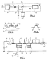
- FIG. 1 Schematically, the detection wafer 1 and the wafer, or chip, for processing 2 of the thermal camera of the invention, which are the essential elements thereof, are represented in FIG. 1.
- the wafers 1, 2 are inserted in a set of other elements which are moreover perfectly known and whose existence will only be briefly recalled here, with reference to FIG. 2.
- the camera comprises, in series, an infrared optic 3, an analysis or scanning system, 4, a focusing lens 5, the detection and processing plates 1, 2, and a display device 6.
- the scanning system 4 essentially comprises a mirror mounted pivoting to scroll the landscape to be analyzed in front of the fixed detectors of the brochure 1.
- the plate 1 comprises a mosaic, or matrix, of nxp infrared detectors 10, arranged in n rows of p detectors.
- the n lines of detectors 10 are arranged differently from the arrangement in FIG. 1, staggered along 2 p columns of not 2 elements.
- the detectors are advantageously photodiodes of mercury cadmium tellurium (Hg Cd Te) each connected to the circuit of the processing wafer 2, which is a silicon circuit. of the charge transfer type, or CCD, or of a similar type.
- the two plates 1 and 2 are superimposed, we are talking about a hybrid component, and the diodes 10 are connected to the circuit of the wafer 2 for example by beams (beam-leads) or other similar connections.
- beams beam-leads
- diode 10ij representing the diode of line i and of column j.
- the diodes of a line are swept successively one after the other.
- the output current (Iij) of each diode (10ij) of each line (i) is processed in an integration and gain control device 11, which delivers a charge signal (Qij) to a delay line 12, in which it undergoes a determined phase shift (Tij).
- the charge signals delivered by all the delay lines 12 associated with the diodes of the same line are added in a summator 13.
- the signals delivered by all the summers 13 associated with the different lines of the detection plate 1 are each processed in an error correction device 14, before being multiplexed in a multiplexer 15, the output signal S of which is sent to the display device 6.
- the delay lines 12 ensure the reshaping of the signals delivered by the detectors of the same line, integrated and controlled, which is necessary due to the geometric dispersion of these detectors.
- each line of detectors comprises only two detectors
- a selection of the best of the two detectors is carried out after multiplexing by appropriate means and, moreover, known.
- the currents (Iij) delivered by the diodes (10ij) are integrated and transformed into the quantity of charges Qij in a integrator 16, of storage (FIG. 3), whose integration time t is controlled by a clock 17 (FIG. 1) delivering a train of pulses H of width t and of period T, the duty cycle t T being variable. Beyond the time t, the currents of the diodes are integrated, over the interval (Tt), in a second integrator 57, for evacuation, called "trash".
- the integration and control device 11 therefore comprises two integrators 16, 57, connected alternately to their associated detection diode by a switch 18 controlled by the clock 17.
- the duty cycle of the clock t T and therefore the integration time t of the storage integrator 16, varies with the average amplitude S of the signal S delivered by the multiplexer 15. This average amplitude is measured in a device 69, connected to the control of variation of the duty cycle of the clock 17.
- the loop of elements 16, 15, 69, 17, 16 forms an automatic gain control loop making it possible to reduce the signal dynamics. When the signal is too high, it is overwritten.
- the quantities of charges (Qij) of the diodes of a line (i) of diodes are added to the adder 13 which delivers an amount of charges Qi from the set of the corresponding line (i), which is processed in the error correction device 14.
- the quantity of charges Qi is transformed into voltage Vi in element 19, by division by a capacitive quantity C, connected to a generator 20 of reference voltage V ref by a connecting capacitor 21 and a switch 22.
- the correction device 14 is connected to the multiplexer 15 at point A, between the capacitor 21 and the switch 22, by another switch 24.
- the diodes of all the lines are shown a uniform reference background 54 (FIG. 2), therefore at a determined temperature.
- the switch 22 is closed and the switch 24 is opened by a device 23, in this case a sensor for the position of the scanning mirror, which fixes the potential of point A to V ref .
- connection capacitor 21 amounts, for line i, to for line l, at Qiref and Qlref, so-called reference charge quantities, being by nature different because of the fixed spatial noise, while the potential V ref is the same for all the lines.
- the link capacitor 21 therefore makes it possible to determine, for each line of detectors, the difference between the quantities of detection charges and the quantities of reference charges.
- a level is determined, here of detection charges, in this case converted into potential level, with respect to a reference level.
- this reference level which is tainted with error, because of the fixed spatial noise, this eliminates this error.
- only the useful part of the information is multiplexed.
- the error correction device 14 therefore makes it possible, for its part, to reduce or cancel the dynamics of fixed spatial noise.
- V ref is determined to be between the maximum and minimum values of Vi.
- the processing board 2 of the camera of the invention is produced in the technology which will now be described.
- FET field effect transistor
- MOS metal oxid semiconductor
- a substrate 30 of one type of conductivity has two doping zones 31 of the other type of conductivity diffused from two openings made in an oxide layer 32.
- Two contact terminals 33 connected to the two doping zones 31 constitute the drain and the source.
- a metal layer 34, on the oxide layer 32 between the two doping openings, constitute the gate, and connected to a third contact terminal, ensures the bias of the transistor.
- the gate 34 When the gate 34 is energized, a space charge is created beneath it which fills in minority carriers the space extending between the two doping zones 31 and which connects the source and the drain 33.33.
- a plate 49, at a transfer potential controlled by the variable duty cycle clock 17, between the plates 44 and 47, above a space 51 in the substrate 40 allows, during the time t mentioned above, transferring the charges from the first well 45 into the second well 48, by creating a charge of space uniting the two wells 45, 48. Beyond the time t, during the interval (Tt), and the action of the plate 49 being inhibited, the remaining charges of the first well 45 flow through the transistor 46 in a second capacitor 50, not shown in the FIG. 7.
- the transistor 46 and this second capacitor 50 constitute the second integrator 57 called evacuation of FIG. 3, the function of the switch 18 of FIG. 3 being ensured by the transfer plate 49.
- FIG. 8 is shown the electrical diagram of elements 40-50.
- the quantity of charges Qij mentioned with reference to FIG. 1 is therefore stored in the well 48. It will be noted that the transistors 41, 46 behave like current generators for the storage of the charges in the capacitors (45, 48) and ( 45.50).
- the silicon wafer has as many input circuits, like the one just described, as there are detection diodes.
- spaced apart electrode plates 60 are placed above the substrate 40, the tensioning of which is effected in a time-shifted manner, to form the delay line 12.
- the charge quantities are converted into voltage, not in the converter 19, but directly at an output diode 61, downstream of the delay plates 60, the diode 61 forming with the substrate 40 a Cij conversion capacity.
- the output cathode of diode 61, under which the quantity of charges Qij is located, is therefore at a potential
- All the output diode cathodes associated respectively with the photodiodes of the same line are connected to each other and to a voltage source V f by means of an FET transistor 62 intended to fix the potential of the cathodes of the diodes 61, if although the potential of the connection line 63 of the cathodes of the diodes 61 is equal to
- each input transistor 68 includes an input diode 70, the cathode 71 of which is voltage-controlled to act as the switch 24 mentioned above and thus ensure multiplexing.
- the transistor 66 performs the function of reference voltage generator 20, also mentioned above, the control of its gate 72 playing the role of the switch 22. It is therefore the sensor 23 of the position of the scanning mirror which controls the gate 72 of the transistor 66 and the cathode 71 of the input diode 70 of the multiplexer. Downstream of the gate 67 of the input transistor 68 of the multiplexer, is arranged a storage and transfer plate 73 for the proper multiplexing of the quantities of potentiated charges Qi, under which extends a storage and transfer well 74. Between the two neighboring transfer plates 73 of two neighboring input transistors 68 of the multiplexer, corresponding to two lines of photodiodes, are arranged isolation electrodes.
- the storage and transfer wells 74 associated with all the lines of photodiodes, respectively, are arranged one after the other. It is only by clock phases applied to the lines 73, that the charges from a well 74 are transferred to the neighboring well, and so on to the outlet well.
- the cathodes 71 are controlled to first saturate the transistors 68 before emptying their storage and transfer well 74 to the level corresponding to the voltage Vi. This is the well-known technique of filling and emptying (spill and fill).
- a gain can be obtained at the input of the multiplexer, because, a voltage being equal to an amount of charges divided by a capacity, it suffices, the voltage remaining constant, to increase the capacity, to increase the quantity of charges.
- the input signals of the multiplexer must have a much greater dynamic than the dispersion of the threshold voltages of its input transistors.
Landscapes
- Engineering & Computer Science (AREA)
- Multimedia (AREA)
- Signal Processing (AREA)
- Transforming Light Signals Into Electric Signals (AREA)
- Solid State Image Pick-Up Elements (AREA)
Claims (12)
- Wärmebildkamera mit Parallelabtastung, umfassend eine Platine (1) mit geradlinig angeordneten Infrarotdetektoren (10) und eine Platine (2) zur Verarbeitung der Detektorsignalen mit Vorrichtungen (11-13), um die Ausgangsströme der Detektoren (10) zu integrierem und erfaßte Ladungssignale zu liefern, welche Detektorladungsmengen entsprechen, die mit jeder der Detektorenreihen verbunden sind, dadurch gekennzeichnet, daß die beiden Platinen übereinander in Form eines Hybrid-Bauteils angeordnet sind und daß die Verarbeitungsplatine (2) Verstärkungskontrollvorrichtungen (69,17), die auf die Amplitude der von der Kamera erfaßten und verarbeiteten und gelieferten Ladungssignale (s) wirken, umfaßt und Vorrichtungen (14) zur Differenzierung zwischen Detektorladungsmengen und mit einem Referenzwert verbundenen Referenzladungsmengen, welche Vorrichtungen (19) zur Umwandlung von Detektorladungen in Spannungen enthalten, die über eine kapazitive Verbindung (21) mit einem Referenzspannungsgenerator (20) verbunden sind, und Vorrichtungen (22,24), welche mit Vorrichtungen (23,54) zusammenwirken, um an den Detektordioden (10) während jedes Abtastrücklaufs bei einer bestimmten Temperatur eine gleichförmige Referenzbasis aufzuweisen und somit für jede Detektorenreihe die Höhe der Referenzladungsmengen für die erfaßten Ladungssignale liefern, wobei die Differenzierungsvorrichtungen (14) dafür ausgelegt sind, daB sie für jede Detektorenreihe die Differenz zwischen den Detektorladungsmengen und den Ladungsmengen bestimmen, die mit dem durch die genannte Basis gebildeten Referenzwert verbunden sind, um die Höhe der Referenzladungen jeder Detektorenreihe als Referenzhöhe zu betrachten und sich so vom umveränderlichen Raumrauschen in dem durch diese Ladungsmengendifferenz dargestellten Ausgangssignal der Kamera zu befreien.
- Kamera gemäß Anspruch 1, bei welcher die genannten Kontrollvorrichtungen Vorrichtungen zur automatische Verstärkungskontrolle sind, welche in Abhängigkeit von der mittleren Amplitude der erfaßten und verarbeiteten Signale die Vorrichtungen (11) zur Integration der Ausgangsströme der Detektoren (10) steuern.
- Kamera gemäß einem der Ansprüche 1 und 2, bei welcher im Anschluß an die Integrationsvorrichtungen (11) Vorrichtungen (12) zur Phasenrücksetzung der von den Detektoren (10) gelieferten, integrierten und kontrollierten Signale vorgesehen sind, um die geometrische Streuung der Detektoren zu beseitigen.
- Kamera gemäß einem der Ansprüche 1 bis 3, bei welcher die Integrationsvorrichtungen (11) einen ersten Lagerungsintegrator (16) und einen zweiten Ausgabeintegrator (57) umfassen, welche alternativ von einem Schalter (18) an ihren angeschlossenen Detektor (10) angeschlossen werden und von den Verstärkungstkontrollvorrichtungen (17,69) gesteuert werden, welche einen Zeitgeber (17) mit in Abhängigkeit von der Amplitude der von der Kamera erfaßten und verarbeiteten und gelieferten Ladungssignale (s) variablem zyklischem Verhältnis beinhalten.
- Kamera gemäß einem der Ansprüch 1 bis 4, bei welcher die von den genannten bzw. mit den verschiedenen Detektorenreihen (10) verbundenen Vorrichtungen zur Bestimmung der Ladungsdifferenzen (14) gelieferten Informationen in einem mit einem Anzeigegerät (6) verbundenen Multiplexer (15) gebündelt werden.
- Kamera gemäß einem der Ansprüche 1 bis 5, bei welcher die Vorrichtungen (11) zur Integration der Ausgangsströme der Detektoren (10) Eingangstransistoren mit Feldeffekt (41) der Verarbeitungsplatine (2) enthalten, welche direkt an ihren jeweiligen Detektor (10) angeschlossen sind.
- Kamera gemäß Anspruch 6, bei welcher die Eingangs-Transistoren mit Feldeffekt (41) in ein Siliziumsubstrat (40) integriert sind, jeder von ihnen einen Lagerungssraum (45) als Drain umfaßt und an jeden von ihnen ein Raum (51) anschließt, welcher mit Hilfe einer Transferplatte (49) mit Minoritätsträgern gefüllt werden kann, und ein zweiter Lagerungsraum (48), wobei der Drain (45) der Eingangstransistoren (41) die Source für Ausgabetransistoren mit Feldeffekt (46) bildet.
- Kamera gemäß Anspruch 7, bei welcher das Potential der Transferplatte (49) von den genannten Verstärkungskontrollvorrichtungen (69-17) kontrolliert wird.
- Kamera gemäß einem der Ansprüche 7 und 8, bei welcher die Kathoden von Ausgangsdioden (61) im Siliziumsubstrat (40) untereinander durch eine Leitung (63) zur Umwandlung von Ladungen in Spannungen verbunden sind.
- Kamera gemäß einem der Ansprüche 7 bis 9, bei welcher das Siliziumsubstrat (40) Multiplex-Transistoren mit Feldeffekt (68) enthält, an deren Gates (67) eine Referenzspannung gelegt werden kann.
- Kamera gemäß Anspruch 10, bei welcher jeder Multiplextransistor (68) eine Eingangsdiode (70) enthält, an deren Kathode eine Multiplexspannung gelegt wird.
- Kamera gemäß Anspruch 11, bei welcher die Spannung der Kathode (71) von Eingangsdioden (70) der Multiplextransistoren (68) und die Spannung ihres Gates (67) von einem Positionsgeber eines Abtastspiegels (4) gesteuert werden.
Applications Claiming Priority (2)
| Application Number | Priority Date | Filing Date | Title |
|---|---|---|---|
| FR8518236A FR2591409B1 (fr) | 1985-12-10 | 1985-12-10 | Camera thermique a balayage parallele |
| FR8518236 | 1985-12-10 |
Publications (2)
| Publication Number | Publication Date |
|---|---|
| EP0230809A1 EP0230809A1 (de) | 1987-08-05 |
| EP0230809B1 true EP0230809B1 (de) | 1992-03-11 |
Family
ID=9325604
Family Applications (1)
| Application Number | Title | Priority Date | Filing Date |
|---|---|---|---|
| EP86402725A Expired - Lifetime EP0230809B1 (de) | 1985-12-10 | 1986-12-09 | Wärmebildkamera mit Parallelabtastung |
Country Status (4)
| Country | Link |
|---|---|
| US (1) | US4771175A (de) |
| EP (1) | EP0230809B1 (de) |
| DE (1) | DE3684292D1 (de) |
| FR (1) | FR2591409B1 (de) |
Families Citing this family (10)
| Publication number | Priority date | Publication date | Assignee | Title |
|---|---|---|---|---|
| GB2204207B (en) * | 1987-04-28 | 1991-03-13 | Rank Xerox Ltd | Thermal imager |
| FR2656186B1 (fr) * | 1988-07-01 | 1996-08-23 | Telecommunications Sa | Procede de liaison d'une plaquette refroidie de pretraitement de signaux et d'une plaquette de traitement et ensemble de traitement pour la mise en óoeuvre du procede. |
| GB2222738B (en) * | 1988-09-07 | 1992-09-23 | Secr Defence | Correction circuit for infrared detectors |
| FR2638309B1 (fr) * | 1988-10-25 | 1996-05-24 | Trefimetaux | Plaquette de pretraitement des courants de sortie de diodes de detection soumises a un rayonnement thermique |
| FR2647203B1 (fr) * | 1989-05-18 | 1995-09-08 | Telecommunications Sa | Ensemble de detection pour systeme de veille infrarouge |
| US5229609A (en) * | 1989-05-18 | 1993-07-20 | Sat (Societe Anonyme De Telecommunications) | Detection assembly for an infrared monitoring system |
| DE69221054T2 (de) * | 1991-09-27 | 1998-01-22 | Texas Instruments Inc | Lese-System und Verfahren für Infrarotdetektoranordnungen |
| FR2714501B1 (fr) * | 1993-12-23 | 1996-01-26 | Thomson Csf | Sommateur de tensions, et mosaïque de sommateurs, pour appareil d'imagerie thermique. |
| US5717608A (en) * | 1994-09-26 | 1998-02-10 | Luxtron Corporation | Electro-optical board assembly for measuring the temperature of an object surface from infra-red emissions thereof, including an automatic gain control therefore |
| JP5182897B2 (ja) * | 2008-01-16 | 2013-04-17 | パナソニック株式会社 | サンプリングフィルタ装置 |
Family Cites Families (14)
| Publication number | Priority date | Publication date | Assignee | Title |
|---|---|---|---|---|
| GB1346954A (en) * | 1972-01-27 | 1974-02-13 | British Aircraft Corp Ltd | Circuits employing camera tubes |
| DE2501934C2 (de) * | 1974-01-25 | 1982-11-11 | Hughes Aircraft Co., Culver City, Calif. | Verfahren zum Betrieb eines ladungsgekoppelten Halbleiter-Bauelementes und ladungsgekoppeltes Halbleiter-Bauelement zur Durchführung dieses Verfahrens |
| US3873836A (en) * | 1974-04-19 | 1975-03-25 | Us Navy | Charge coupled radiation detector imaging system |
| US4031393A (en) * | 1976-03-18 | 1977-06-21 | The United States Of America As Represented By The Secretary Of The Army | Thermal image camera |
| US4054797A (en) * | 1976-09-23 | 1977-10-18 | The United States Of America As Represented By The Secretary Of The Navy | Series-parallel scan, IR, CID, focal-plane array |
| US4286278A (en) * | 1977-09-01 | 1981-08-25 | Honeywell Inc. | Hybrid mosaic IR/CCD focal plane |
| US4143269A (en) * | 1977-12-19 | 1979-03-06 | Texas Instruments Incorporated | Ferroelectric imaging system |
| US4178522A (en) * | 1978-03-15 | 1979-12-11 | General Electric Company | Infrared detection apparatus |
| US4337395A (en) * | 1978-10-13 | 1982-06-29 | Hughes Aircraft Company | Monolithic imager |
| US4225883A (en) * | 1979-06-11 | 1980-09-30 | The United States Of America As Represented By The Secretary Of The Army | Automatic responsivity compensator in an IR imaging system |
| US4390785A (en) * | 1980-12-29 | 1983-06-28 | E. I. Du Pont De Nemours & Co. | Method and apparatus for remotely detecting gases in the atmosphere |
| US4399464A (en) * | 1981-05-04 | 1983-08-16 | General Dynamics, Pomona Division | Signal processor for an array of CID radiation detector elements |
| US4403148A (en) * | 1981-05-07 | 1983-09-06 | Optic-Electronic Corporation | Electro-optical scanning and display system |
| FR2548498B1 (fr) * | 1983-06-28 | 1985-10-18 | Thomson Csf | Procede de correction du niveau en sortie d'un dispositif a transfert de charge et dispositif pour sa mise en oeuvre |
-
1985
- 1985-12-10 FR FR8518236A patent/FR2591409B1/fr not_active Expired
-
1986
- 1986-12-08 US US06/938,882 patent/US4771175A/en not_active Expired - Fee Related
- 1986-12-09 DE DE8686402725T patent/DE3684292D1/de not_active Expired - Fee Related
- 1986-12-09 EP EP86402725A patent/EP0230809B1/de not_active Expired - Lifetime
Also Published As
| Publication number | Publication date |
|---|---|
| DE3684292D1 (de) | 1992-04-16 |
| FR2591409B1 (fr) | 1988-08-19 |
| FR2591409A1 (fr) | 1987-06-12 |
| EP0230809A1 (de) | 1987-08-05 |
| US4771175A (en) | 1988-09-13 |
Similar Documents
| Publication | Publication Date | Title |
|---|---|---|
| EP0237365B1 (de) | Lichtempfindliche Vorrichtung | |
| EP0474550B1 (de) | Bilddetektor mit Grossformat-Pixels | |
| EP0783227A2 (de) | Vorrichtung zum Auslesen einer Bildpunktmatrix unter Verwendung von TDI | |
| EP0230809B1 (de) | Wärmebildkamera mit Parallelabtastung | |
| EP0435773B1 (de) | Bildaufnahmeeinrichtung mit integrierten Ablenkschaltungen | |
| WO2008034677A1 (fr) | Capteur d'image lineaire cmos a fonctionnement de type transfert de charges | |
| EP0331546B1 (de) | Photoempfindlicher Matrix mit zwei Dioden pro Punkt ohne spezifischen Rückstellungsleiter | |
| EP0491596B1 (de) | Monolithischer Infrarotdetektor aus pyroelektrischem Material | |
| FR2704095A1 (fr) | Capteur d'images du type dispositif à couplage de charge. | |
| FR2621200A1 (fr) | Appareil de prise de vues du type monolithique a semiconducteurs | |
| EP1627432B1 (de) | Cmos bildaufnahmevorrichtung | |
| EP0148086B1 (de) | Hintergrundladungsbeseitigung in einer lichtempfindlichen Festkörperanordnung | |
| EP0323924B1 (de) | Leseverfahren und Schaltung mit niedrigem Geräusch für photosensitive Zeilentransfermatrix | |
| FR2511545A1 (fr) | Dispositif semi-conducteur comportant un dispositif a couplage de charges a quatre phases | |
| EP0958545B1 (de) | Integratorschaltung von photoerzeugten ladungen mit verbesserter linearität | |
| FR2855913A1 (fr) | Reseau de condensateurs de stockage pour dispositif d'imagerie a l'etat solide | |
| EP0031751B1 (de) | Ladungstransportgenerator kodierter Spannung; mit solchem Ladungstransportgenerator ausgerüsteter Analog-Digital-Kodierer und -Dekodierer | |
| EP0129470A1 (de) | Festkörper photoempfindliche Anordnung | |
| EP1425903A1 (de) | Steuerungsverfahren einer photoempfindlichen vorrichtung | |
| EP0654945B1 (de) | Ladungseinspritzschaltung zur thermischen Abbildung | |
| EP0749234A1 (de) | Halbleiter-Bildsensor mit integrierte Pixelhistogrammumwandlung | |
| FR2751155A1 (fr) | Dispositif de lecture pour une mosaique de detecteurs electromagnetiques, et systeme de detection equipe d'un tel dispositif | |
| EP0275740B1 (de) | Ausleseschaltung für eine lichtempfindliche Zeilenübertragungsanordnung, lichtempfindliche Zeilenübertragungsanordnung mit einer solchen Schaltung und Ausleseverfahren einer solchen Anordnung | |
| FR2682813A1 (fr) | Dispositif de visualisation de rayonnements infra-rouges. | |
| FR2672759A1 (fr) | Capteur d'images a semiconducteurs, a stockage de charge. |
Legal Events
| Date | Code | Title | Description |
|---|---|---|---|
| PUAI | Public reference made under article 153(3) epc to a published international application that has entered the european phase |
Free format text: ORIGINAL CODE: 0009012 |
|
| AK | Designated contracting states |
Kind code of ref document: A1 Designated state(s): BE DE GB NL SE |
|
| 17P | Request for examination filed |
Effective date: 19871217 |
|
| 17Q | First examination report despatched |
Effective date: 19900409 |
|
| GRAA | (expected) grant |
Free format text: ORIGINAL CODE: 0009210 |
|
| AK | Designated contracting states |
Kind code of ref document: B1 Designated state(s): BE DE GB NL SE |
|
| REF | Corresponds to: |
Ref document number: 3684292 Country of ref document: DE Date of ref document: 19920416 |
|
| GBT | Gb: translation of ep patent filed (gb section 77(6)(a)/1977) | ||
| PLBE | No opposition filed within time limit |
Free format text: ORIGINAL CODE: 0009261 |
|
| STAA | Information on the status of an ep patent application or granted ep patent |
Free format text: STATUS: NO OPPOSITION FILED WITHIN TIME LIMIT |
|
| 26N | No opposition filed | ||
| EAL | Se: european patent in force in sweden |
Ref document number: 86402725.5 |
|
| PGFP | Annual fee paid to national office [announced via postgrant information from national office to epo] |
Ref country code: SE Payment date: 19991119 Year of fee payment: 14 |
|
| PGFP | Annual fee paid to national office [announced via postgrant information from national office to epo] |
Ref country code: NL Payment date: 19991122 Year of fee payment: 14 |
|
| PGFP | Annual fee paid to national office [announced via postgrant information from national office to epo] |
Ref country code: GB Payment date: 19991206 Year of fee payment: 14 |
|
| PGFP | Annual fee paid to national office [announced via postgrant information from national office to epo] |
Ref country code: DE Payment date: 19991229 Year of fee payment: 14 |
|
| PGFP | Annual fee paid to national office [announced via postgrant information from national office to epo] |
Ref country code: BE Payment date: 20000106 Year of fee payment: 14 |
|
| PG25 | Lapsed in a contracting state [announced via postgrant information from national office to epo] |
Ref country code: GB Free format text: LAPSE BECAUSE OF NON-PAYMENT OF DUE FEES Effective date: 20001209 |
|
| PG25 | Lapsed in a contracting state [announced via postgrant information from national office to epo] |
Ref country code: SE Free format text: LAPSE BECAUSE OF NON-PAYMENT OF DUE FEES Effective date: 20001210 |
|
| PG25 | Lapsed in a contracting state [announced via postgrant information from national office to epo] |
Ref country code: BE Free format text: LAPSE BECAUSE OF NON-PAYMENT OF DUE FEES Effective date: 20001231 |
|
| BERE | Be: lapsed |
Owner name: S.A. SAT DE TELECOMMUNICATIONS Effective date: 20001231 |
|
| PG25 | Lapsed in a contracting state [announced via postgrant information from national office to epo] |
Ref country code: NL Free format text: LAPSE BECAUSE OF NON-PAYMENT OF DUE FEES Effective date: 20010701 |
|
| GBPC | Gb: european patent ceased through non-payment of renewal fee |
Effective date: 20001209 |
|
| EUG | Se: european patent has lapsed |
Ref document number: 86402725.5 |
|
| NLV4 | Nl: lapsed or anulled due to non-payment of the annual fee |
Effective date: 20010701 |
|
| PG25 | Lapsed in a contracting state [announced via postgrant information from national office to epo] |
Ref country code: DE Free format text: LAPSE BECAUSE OF NON-PAYMENT OF DUE FEES Effective date: 20011002 |