EP0238162A2 - Optisches Informationswiedergabegerät - Google Patents
Optisches Informationswiedergabegerät Download PDFInfo
- Publication number
- EP0238162A2 EP0238162A2 EP87300310A EP87300310A EP0238162A2 EP 0238162 A2 EP0238162 A2 EP 0238162A2 EP 87300310 A EP87300310 A EP 87300310A EP 87300310 A EP87300310 A EP 87300310A EP 0238162 A2 EP0238162 A2 EP 0238162A2
- Authority
- EP
- European Patent Office
- Prior art keywords
- phase difference
- tracking error
- signal
- delaying
- output signal
- Prior art date
- Legal status (The legal status is an assumption and is not a legal conclusion. Google has not performed a legal analysis and makes no representation as to the accuracy of the status listed.)
- Granted
Links
Images

Classifications
-
- G—PHYSICS
- G11—INFORMATION STORAGE
- G11B—INFORMATION STORAGE BASED ON RELATIVE MOVEMENT BETWEEN RECORD CARRIER AND TRANSDUCER
- G11B7/00—Recording or reproducing by optical means, e.g. recording using a thermal beam of optical radiation by modifying optical properties or the physical structure, reproducing using an optical beam at lower power by sensing optical properties; Record carriers therefor
- G11B7/08—Disposition or mounting of heads or light sources relatively to record carriers
- G11B7/09—Disposition or mounting of heads or light sources relatively to record carriers with provision for moving the light beam or focus plane for the purpose of maintaining alignment of the light beam relative to the record carrier during transducing operation, e.g. to compensate for surface irregularities of the latter or for track following
- G11B7/095—Disposition or mounting of heads or light sources relatively to record carriers with provision for moving the light beam or focus plane for the purpose of maintaining alignment of the light beam relative to the record carrier during transducing operation, e.g. to compensate for surface irregularities of the latter or for track following specially adapted for discs, e.g. for compensation of eccentricity or wobble
-
- G—PHYSICS
- G11—INFORMATION STORAGE
- G11B—INFORMATION STORAGE BASED ON RELATIVE MOVEMENT BETWEEN RECORD CARRIER AND TRANSDUCER
- G11B7/00—Recording or reproducing by optical means, e.g. recording using a thermal beam of optical radiation by modifying optical properties or the physical structure, reproducing using an optical beam at lower power by sensing optical properties; Record carriers therefor
- G11B7/08—Disposition or mounting of heads or light sources relatively to record carriers
- G11B7/09—Disposition or mounting of heads or light sources relatively to record carriers with provision for moving the light beam or focus plane for the purpose of maintaining alignment of the light beam relative to the record carrier during transducing operation, e.g. to compensate for surface irregularities of the latter or for track following
- G11B7/094—Methods and circuits for servo offset compensation
-
- G—PHYSICS
- G11—INFORMATION STORAGE
- G11B—INFORMATION STORAGE BASED ON RELATIVE MOVEMENT BETWEEN RECORD CARRIER AND TRANSDUCER
- G11B7/00—Recording or reproducing by optical means, e.g. recording using a thermal beam of optical radiation by modifying optical properties or the physical structure, reproducing using an optical beam at lower power by sensing optical properties; Record carriers therefor
- G11B7/08—Disposition or mounting of heads or light sources relatively to record carriers
- G11B7/09—Disposition or mounting of heads or light sources relatively to record carriers with provision for moving the light beam or focus plane for the purpose of maintaining alignment of the light beam relative to the record carrier during transducing operation, e.g. to compensate for surface irregularities of the latter or for track following
- G11B7/0901—Disposition or mounting of heads or light sources relatively to record carriers with provision for moving the light beam or focus plane for the purpose of maintaining alignment of the light beam relative to the record carrier during transducing operation, e.g. to compensate for surface irregularities of the latter or for track following for track following only
-
- G—PHYSICS
- G11—INFORMATION STORAGE
- G11B—INFORMATION STORAGE BASED ON RELATIVE MOVEMENT BETWEEN RECORD CARRIER AND TRANSDUCER
- G11B7/00—Recording or reproducing by optical means, e.g. recording using a thermal beam of optical radiation by modifying optical properties or the physical structure, reproducing using an optical beam at lower power by sensing optical properties; Record carriers therefor
- G11B7/08—Disposition or mounting of heads or light sources relatively to record carriers
- G11B7/09—Disposition or mounting of heads or light sources relatively to record carriers with provision for moving the light beam or focus plane for the purpose of maintaining alignment of the light beam relative to the record carrier during transducing operation, e.g. to compensate for surface irregularities of the latter or for track following
- G11B7/0908—Disposition or mounting of heads or light sources relatively to record carriers with provision for moving the light beam or focus plane for the purpose of maintaining alignment of the light beam relative to the record carrier during transducing operation, e.g. to compensate for surface irregularities of the latter or for track following for focusing only
- G11B7/0909—Disposition or mounting of heads or light sources relatively to record carriers with provision for moving the light beam or focus plane for the purpose of maintaining alignment of the light beam relative to the record carrier during transducing operation, e.g. to compensate for surface irregularities of the latter or for track following for focusing only by astigmatic methods
Definitions
- This invention relates to an optical information reproducing apparatus which optically reads an information from a recording medium, and more particularly to its tracking control.
- phase difference tracking method This phase difference tracking method is disclosed, for example, in Japanese Pat. Appln. of laid-open No. 52-93222. The method can substantially solve the problem previously mentioned.
- the far field image formed on the photodetector is asymmetrically displaced with respect to the first straight line, the tangential phase difference is not canceled to become the offset of the tracking error signal.
- the offset of the tracking error signal varies in a direction to increase the tracking error.
- a bias of an objective lens in the radial direction causes the offset of the tracking error signal develop to cause a positive feedback so as to further expand the bias.
- An object of the present indention is to provide an optical information reproducing apparatus in which the offset of tracking error signal varies little even if the image on a photodetector is displaced when reading an information from a recording medium where the information is recorded as succession of pits which have a phase depth different from an integral number times a quarter wave length.
- the optical information reproducing apparatus by the present invention is comprised as follows.
- the far field image of a light spot by a detecting light from a recording medium is divided into four quadrants by a first straight line substantially parallel to a direction in which an information track is extended and a second straight line substantially perpendicular to the direction so that four photocells can receive lights incident on the four quadrants respectively.
- a tracking error is detected according to at least one of two phase differences: a phase difference between outputs from the photocells at the first and second quadrants located on one side divided by the second straight line; and a phase difference between outputs from the photocells at the third and fourth quadrants located on the other side divided by said second straight line.
- a tracking error is detected according to a phase difference between a sum of a signal, which is outputted from the photocell at the first quadrant photocell and delayed for a specified time and a signal which is outputted from the photocell at the third quadrant photocell and a sum of a signal, which is outputted from the photocell at the second quadrant photocell and delayed for a specified time and a signal which is outputted from the photocell at the fourth quadrant photocell.
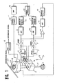
- an irradiation beam 21 radiated from a semiconductor laser 1 and passed through a beam splitter 2 is converged on a recording medium 20 by an objective lens 3 to form a light spot.
- the reflected light from the recording medium 20 is collected by the objective lens 3 to be a detecting beam 22.
- the detecting beam 22 is reflected by the beam splitter 2 and separated from the irradiation beam 21.
- the detecting beam 22 is provided with astigmatism by a cylindrical lens 4, and then forms a far field image of the light spot on a photodetector 5.
- the photodetector 5 is divided into four quadrants by two straight lines parallel to Z and X directions in the figure, and receives respective parts of the far field image incident on the four quadrants by photocells 5a, 5b, 5c and 5d respectively to output signals corresponding to the received light quantity.
- Delaying circuits 6 and 7 delay the output signals from photocells 5a and 5b so as to cancel the offset of the tangential phase difference.
- An adder 8 adds an output signal current from the delay circuit 6 and that from the photocell 5c, and converts the resultant current to a voltage.
- An adder 9 adds an output signal current from the delaying circuit 7 and that from the photocell 5d, and converts the resultant current to a voltage.
- a phase comparator 12 can detect tracking error by comparing phases of the output signals of the adder 8 and the adder 9.
- high frequency componets are extracted by means of high-pass filters 70 and 71 for removing low frequency noises from the recording medium, and shaped in waveform by means of waveform shapers 10 and 11 for making the phase comparison easy.
- the offset of the tangential phase difference is removed by the delaying circuits 6 and 7, thus providing a correct detection of tracking error even if the far field image is displaced on the photodetector 5.
- a low-pass filter 13 removes ripple component from the output signal of the phase comparator 12 to obtain a tracking error signal.
- a tracking control circuit 14 drives an actuator 18 in response to the tracking error signal to control the position of the objective lens 3. Tracking control is performed in this manner.
- the detecting beam 22 is provided with astigmatism, allowing a focussing error to be detected by a difference between the quantity of light incident on the photocells 5a and 5c and that incident on the photocells 5b and 5d.
- Such a focussing error detecting method is known as disclosed in U.S. Pat. No. 4,023,033.
- a differential amplifier 15 outputs a signal corresponding to a difference between the output signals of the adder 8 and the adder 9.
- a low-pass filter 16 removes ripple component from this output signal to obtain a focussing error signal.
- a focussing control circuit 17 drives the actuator 18 in response to the focussing error signal to control the position of the objective lens 3. Focussing control is performed in this manner. With such a manner, both of the focussing error and tracking error can be detected from the same two signals which are output from the photodetector 5: the former from the level difference, and the latter from the phase difference. Accordingly, the photodetector 5 can be composed of only four photocells and the adders 8 and 9 also be used in common for the two error detections.
- a preamplifier 19 amplifies a sum signal of all of the photocells from an injection current into the substrate of the photodetector 5 to obtain an information signal.
- the delaying circuits 6 and 7 are each composed of a low-pass filter having capacitor and resistor as shown in the figure, the frequency characteristic of the information signal will not be deteriorated.
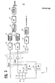
- Fig. 2 shows another embodiment of the invention provided with improved delaying circuits.
- the delaying circuits 6 and 7 are adapted such that the output signals of the photocells 5a and 5b are delayed for a specified time.
- the range of the phase depth of the pits on the recording medium is limited because a variation in the tangential phase difference causes a variation in the optimum value of the delaying time.
- the delaying time of the delaying circuits is adaptively controlled so as to obtain the effect of this invention even if the phase depth of the pits varies.
- Variable delaying circuits 30 and 31 are adapted such that the delaying time is changed by means of a delaying time controller 44.
- the delaying time controller 44 controls the delaying time as follows.
- Buffer amplifiers 32 and 33 convert the respective signal currents from the variable delaying circuits 30 and 31 into voltages.
- Buffer amplifiers 34 and 35 directly convert the respective signal currents from the photocells 5c and 5d into voltages.
- Output signals from the buffer amplifiers 32 and 33 are added to each other by an adder 38, and output signals from the buffer amplifiers 34 and 35 are added to each other by an adder 39.
- a phase difference remains in output signals from the adders 38 and 39.
- this phase difference of the output signals from the adders 38 and 39 detected by means of a phase comparator 42 corresponds to an error in the delaying time of the variable delaying circuits 30 and 31.
- High pass filters 72 and 73, and waveform shapers 40 and 41 function similarly to the high pass filters 70 and 71, and the waveform shapers 10 and 11 in Fig. 1.
- An integrator 43 integrates a signal corresponding to the error in the delaying time from the phase comparator 42.
- the delaying time controller 44 changes the relaying time of the variable delaying circuits 30 and 31. In this manner, the variable delaying circuits 30 and 31 are controlled so as to precisely cancel the tangential phase difference.
- An adder 36 adds the signal which is outputted from the photocell 5a and delayed by the delaying circuit 10 to the output signal from the photocell 5c.
- An adder 37 adds the signal which is outputted from the photocell 5b and delayed by the delaying circuit 31 to the ouput signal from the photocell 5d. Tracking error is detected from a phase difference between output signals from the adders 36 and 37 similarly to the case in Fig. 1
- the delaying time of the circuits 30 and 31 is designed to be changed discretely. If a sufficient matching of the delaying time is provided, the delaying circuits may be adapted such that the delaying time can be continuously changed.
- the tangential phase difference is precisely canceled in the above embodiment, it is not always necessary to precisely cancel the tangential phase difference.
- the tangential phase difference may be reduced to such an extent that the unstability of tracking control is eliminated.
- the offset of the tracking error signal resulting from the movement of the far field image on the photodetector 5 according to the movement of the objective lens for tracking often causes the tracking control to be in unstable condition as previously described. Accordingly the delaying time of the variable delaying circuits 30 and 31 may be adjusted so as to excessively cancel the offset of the tangential phase difference.
- the offset of the tracking error signal developing when the objective lens 3 is biased for tracking control is placed in a direction of negative feedback so as to cancel the bias of the objective lens 3.
- the tracking control system and the carriage will not run away.
- F ig. 3 shows a block diagram of a major part of still another embodiment of the invention.
- a delaying circuit is provided to cancel the tangential phase difference, while this Fig. 3 embodiment removes the influence of the tangential phase difference by a different manner. That is, this embodiment detects a tracking error by only the phase difference between the quantity change of light incident on the first quadrant and that of light incident on the second quadrant.
- Low-pass filters 60 and 61 remove such high frequency components as to pass through the high-pass filters 70 and 71 from the output signals of the third quadrant photocell 5c and the fourth quadrant photocell 5d respectively.
- the adder 8 adds an output signal current from the low-pass-filter, 60 and an output signal current from the first quadrant photocell 5a, and converts the sum signal current into a voltage.
- the adder 9 adds an output signal current from the low-pass filter 61 and an output signal current from the second quadrant photocell 5b, and converts the sum signal current into a voltage.
- Output signals from the adders 8 and 9 are passed through the high-pass filters 70 and 71 so that low frequency components are removed, and then are shaped in waveforms by the waveform shapers 10 and 11.
- the phase difference between output signals of the waveform shapers 10 and 11 substantially becomes the same as the phase difference between the quantity change of light incident on the first quadrant and that of light incident on the second quadrant. This is because the signal components corresponding to the quantities of lights incident on the third and fourth quadrants are almost removed by the low-pass filters 60 and 61, and by the high-pass filters 70 and 71. Thus, the phase difference corresponding to the tracking error can be detected from the output signals of the waveform shapers 10 and 11 by the phase comparator 12.
- the output signal of the adder 8 contains a sum of low frequency components of the output signals from the photocells 5a and 5c
- the output signal of the adder 9 contains a sum of low frequency components of the output signals from the photocells 5b and 5d.
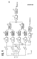
- Fig. 4 shows a block diagram of a major part of yet another embodiment of the invention.
- buffer amplifiers 32, 33, 34 and 35 convert the output signal currents from the photocells 5a, 5b, 5c and 5d into voltages.
- Output signals from the buffer amplifiers 32 and 33 are passed through high pass filters 74 and 75 so that low frequency components are removed, shaped in waveform by waveform shapers 50 and 51, and then compared of their phases by -a phase comparator 54. In this manner., tracking error is detected similarly to the case in Fig. 3.
- tracking error is similarly detected also by buffer amplifiers 34 and 35, high-pass filters 76 and 77, and a phase comparator 55.
- a more stable and less noisy tracking error signal than the case in Fig. 3 can be obtained.
- the tracking error is independently detected by the phase difference between the quantity changes of lights incident on the first and second quadrants and by the phase difference between the quantity changes of lights incident on the third and fourth quadrants,- the influence of the tangential phase difference can be eliminated. Therefore, the variation in the offset of tracking error detection can be made small even if the objective lens is displaced for tracking control.
- the present invention specifically provides an apparatus to reduce the variation in the offset of tracking error developing when the objective lens is displaced due to eccentricity and the like of a recording medium for tracking error detection by the phase difference tracking method, on the basis of a discovery that the variation results from the tangential phase difference.
Landscapes
- Optical Recording Or Reproduction (AREA)
Applications Claiming Priority (2)
| Application Number | Priority Date | Filing Date | Title |
|---|---|---|---|
| JP61006711A JPH063648B2 (ja) | 1986-01-16 | 1986-01-16 | 光学的情報再生装置 |
| JP6711/86 | 1986-01-16 |
Publications (3)
| Publication Number | Publication Date |
|---|---|
| EP0238162A2 true EP0238162A2 (de) | 1987-09-23 |
| EP0238162A3 EP0238162A3 (en) | 1988-06-22 |
| EP0238162B1 EP0238162B1 (de) | 1992-03-18 |
Family
ID=11645868
Family Applications (1)
| Application Number | Title | Priority Date | Filing Date |
|---|---|---|---|
| EP87300310A Expired - Lifetime EP0238162B1 (de) | 1986-01-16 | 1987-01-15 | Optisches Informationswiedergabegerät |
Country Status (5)
| Country | Link |
|---|---|
| US (1) | US4785441A (de) |
| EP (1) | EP0238162B1 (de) |
| JP (1) | JPH063648B2 (de) |
| KR (1) | KR900004620B1 (de) |
| DE (1) | DE3777426D1 (de) |
Cited By (5)
| Publication number | Priority date | Publication date | Assignee | Title |
|---|---|---|---|---|
| EP0803865A1 (de) * | 1996-04-22 | 1997-10-29 | Kabushiki Kaisha Toshiba | Schaltung zur Erzeugung eines Spurfolgefehlersignals |
| EP0895227A1 (de) * | 1997-07-31 | 1999-02-03 | THOMSON multimedia | Spurfolgesystem für optische Speichermedien |
| EP0822542A3 (de) * | 1996-07-31 | 1999-11-10 | Deutsche Thomson-Brandt Gmbh | Gerät zum Lesen und/oder Beschreiben optischer Aufzeichnungsträger |
| EP0895228A3 (de) * | 1997-07-31 | 1999-11-24 | THOMSON multimedia S.A. | Spurfolgesystem für optische Speichermedien |
| EP0930612A3 (de) * | 1998-01-16 | 2000-05-03 | Mitsubishi Denki Kabushiki Kaisha | Verfahren und Vorrichtung zur Wiedergabe von optischen Informationen |
Families Citing this family (26)
| Publication number | Priority date | Publication date | Assignee | Title |
|---|---|---|---|---|
| JP2614482B2 (ja) * | 1988-03-11 | 1997-05-28 | 三洋電機株式会社 | 光学式デイスクプレーヤの信号再生回路 |
| US5138594A (en) * | 1990-04-20 | 1992-08-11 | International Business Machines Corporation | Reducing amplitude variations of optical disk readback signals and increasing reliability of track-crossing counts |
| JPH07296395A (ja) * | 1994-04-27 | 1995-11-10 | Victor Co Of Japan Ltd | 情報再生装置のトラッキング信号検出方法 |
| JP3336778B2 (ja) * | 1994-11-25 | 2002-10-21 | 松下電器産業株式会社 | トラッキング誤差検出装置 |
| TW364992B (en) * | 1996-04-25 | 1999-07-21 | Toshiba Corp | Optic data regeneration apparatus and control method thereof |
| DE19627383A1 (de) * | 1996-07-06 | 1998-01-08 | Thomson Brandt Gmbh | Gerät zum Lesen oder Beschreiben optischer Aufzeichnungsträger |
| US5914925A (en) * | 1997-01-10 | 1999-06-22 | Eastman Kodak Company | DRDW differential phase tracking method and apparatus |
| TW449736B (en) | 1997-04-14 | 2001-08-11 | Matsushita Electric Industrial Co Ltd | Optical disk drive apparatus |
| DE19723542A1 (de) | 1997-06-05 | 1998-12-10 | Thomson Brandt Gmbh | Gerät zum Lesen und/oder Beschreiben optischer Aufzeichnungsträger |
| US6088388A (en) * | 1997-09-16 | 2000-07-11 | Tektronix, Inc. | Digital fir filters for compensation of nyquist slope in pseudo-synchronous demodulators |
| TW412738B (en) | 1998-03-09 | 2000-11-21 | Koninkl Philips Electronics Nv | Optical read/write apparatus |
| KR100524902B1 (ko) * | 1998-06-12 | 2005-12-21 | 삼성전자주식회사 | 불량 파형 검출 기능을 갖는 트래킹 에러 검출장치 |
| EP1034537A2 (de) * | 1998-06-15 | 2000-09-13 | Koninklijke Philips Electronics N.V. | Anordnung zum abtasten eines optischen aufzeichnungsträgers |
| US6781104B1 (en) | 1998-06-16 | 2004-08-24 | Koninklijke Philips Electronics N.V. | Device for scanning an optical record carrier |
| DE19852291A1 (de) * | 1998-11-13 | 2000-05-18 | Thomson Brandt Gmbh | Gerät zum Lesen und/oder Beschreiben optischer Aufzeichnungsträger |
| JP3439393B2 (ja) * | 1999-08-30 | 2003-08-25 | 松下電器産業株式会社 | トラッキング誤差検出装置 |
| JP4578656B2 (ja) * | 1999-09-16 | 2010-11-10 | 三星電子株式会社 | 光記録再生機器用エラー信号検出装置 |
| JP3968984B2 (ja) * | 2000-10-05 | 2007-08-29 | 三菱電機株式会社 | 光ディスク再生装置およびディスク種別判別方法 |
| KR100396544B1 (ko) * | 2000-11-17 | 2003-09-02 | 삼성전자주식회사 | 광기록재생기기용 에러신호 검출장치 |
| FR2837972B1 (fr) * | 2002-04-02 | 2006-07-21 | Thales Sa | Procede d'asservissement radial pour un dispositif de reproduction d'informations d'un disque optique et dispositif de reproduction mettant en oeuvre ce procede |
| JP2004259403A (ja) * | 2003-02-27 | 2004-09-16 | Toshiba Corp | ディスク装置及び信号処理方法 |
| TWI248610B (en) * | 2003-04-07 | 2006-02-01 | Mediatek Inc | Method and related apparatus for deriving a tracking error signal |
| US7512043B2 (en) * | 2004-07-08 | 2009-03-31 | Realtek Semiconductor Corp. | Apparatus and method for generating a tracking error signal in an optical disc drive |
| TWI258740B (en) * | 2004-07-08 | 2006-07-21 | Realtek Semiconductor Corp | Apparatus and method for generating a tracking error signal in an optical disc drive |
| US7583569B2 (en) * | 2004-07-08 | 2009-09-01 | Realtek Semiconductor Corp. | Apparatus and related method for generating a tracking error signal in an optical disc drive |
| US7633842B2 (en) * | 2004-07-08 | 2009-12-15 | Realtek Semiconductor Corp. | Apparatus for generating tracking error signal in optical disc drive |
Family Cites Families (6)
| Publication number | Priority date | Publication date | Assignee | Title |
|---|---|---|---|---|
| FR2271590B1 (de) * | 1974-01-15 | 1978-12-01 | Thomson Brandt | |
| US4057833A (en) * | 1974-10-03 | 1977-11-08 | U.S. Philips Corporation | Centering detection system for an apparatus for playing optically readable record carriers |
| FR2325987A1 (fr) * | 1975-09-29 | 1977-04-22 | Thomson Brandt | Dispositif de lecture optique d'un enregistrement |
| NL8000122A (nl) * | 1980-01-09 | 1981-08-03 | Philips Nv | Schijfvormige, optisch uitleesbare registratiedrager als opslagmedium voor datainformatie, inrichting voor het vervaardigen van zo'n registratiedrager, inrichting voor het optekenen en/of weergeven van datainformatie in c.q. van zo'n registratiedrager. |
| NL8103505A (nl) * | 1981-07-24 | 1983-02-16 | Philips Nv | Inrichting voor het puntsgewijs aftasten van een voorwerp. |
| JPS5891538A (ja) * | 1981-11-25 | 1983-05-31 | Hitachi Ltd | 光デイスクトラツク追跡装置 |
-
1986
- 1986-01-16 JP JP61006711A patent/JPH063648B2/ja not_active Expired - Lifetime
-
1987
- 1987-01-15 KR KR1019870000259A patent/KR900004620B1/ko not_active Expired
- 1987-01-15 EP EP87300310A patent/EP0238162B1/de not_active Expired - Lifetime
- 1987-01-15 DE DE8787300310T patent/DE3777426D1/de not_active Expired - Lifetime
- 1987-01-16 US US07/004,139 patent/US4785441A/en not_active Expired - Lifetime
Cited By (8)
| Publication number | Priority date | Publication date | Assignee | Title |
|---|---|---|---|---|
| EP0803865A1 (de) * | 1996-04-22 | 1997-10-29 | Kabushiki Kaisha Toshiba | Schaltung zur Erzeugung eines Spurfolgefehlersignals |
| US5859816A (en) * | 1996-04-22 | 1999-01-12 | Kabushiki Kaisha Toshiba | Tracking error signal generating circuit |
| EP0822542A3 (de) * | 1996-07-31 | 1999-11-10 | Deutsche Thomson-Brandt Gmbh | Gerät zum Lesen und/oder Beschreiben optischer Aufzeichnungsträger |
| EP0895227A1 (de) * | 1997-07-31 | 1999-02-03 | THOMSON multimedia | Spurfolgesystem für optische Speichermedien |
| EP0895228A3 (de) * | 1997-07-31 | 1999-11-24 | THOMSON multimedia S.A. | Spurfolgesystem für optische Speichermedien |
| US6205094B1 (en) | 1997-07-31 | 2001-03-20 | Thomson Licensing S.A. | Tracking system for optical storage media |
| EP0930612A3 (de) * | 1998-01-16 | 2000-05-03 | Mitsubishi Denki Kabushiki Kaisha | Verfahren und Vorrichtung zur Wiedergabe von optischen Informationen |
| US6339567B1 (en) | 1998-01-16 | 2002-01-15 | Mitsubishi Denki Kabushiki Kaisha | Method of and apparatus for optical information reproduction |
Also Published As
| Publication number | Publication date |
|---|---|
| US4785441A (en) | 1988-11-15 |
| KR870007491A (ko) | 1987-08-19 |
| EP0238162B1 (de) | 1992-03-18 |
| KR900004620B1 (ko) | 1990-06-30 |
| EP0238162A3 (en) | 1988-06-22 |
| JPH063648B2 (ja) | 1994-01-12 |
| DE3777426D1 (de) | 1992-04-23 |
| JPS62165737A (ja) | 1987-07-22 |
Similar Documents
| Publication | Publication Date | Title |
|---|---|---|
| US4785441A (en) | Tracking error correction apparatus utilizing phase difference information derived from four photocells | |
| JP2734054B2 (ja) | 光ディスク装置のトラッキングエラー検出装置及びトラッキングエラー検出方法 | |
| KR100210543B1 (ko) | 트랙킹 에라 신호 발생기 | |
| US4815060A (en) | Optical pickup device with tracking and focusing utilizing a photodetector having four regions | |
| KR100302447B1 (ko) | 광학식기록재생장치 | |
| JPS61188745A (ja) | フオ−カスサ−ボ制御方式 | |
| JPH0664746B2 (ja) | 光スポット位置検出装置 | |
| JPH04313818A (ja) | アクチュエータ位置検出装置、アクチュエータ位置制御装置及びトラックサーチ制御装置 | |
| US5399849A (en) | Focusing control apparatus for an optical disk system employing a gain adjusted and phase compensated error signal | |
| JP4284725B2 (ja) | 光学記録媒体からの読み出し又は該媒体への書き込みのための装置 | |
| US5471446A (en) | Optical disk player having beam correction means | |
| JP2001155352A (ja) | 光ディスク記録/再生装置のレーザースポット移動方向判別のための方向判別信号発生方法及びこれを用いたレーザースポット移動方向判断方法そしてこれに適した装置 | |
| JPH10112042A (ja) | 光学的情報再生装置 | |
| JP2640529B2 (ja) | 光ディスクプレーヤ | |
| JPS6252735A (ja) | 光学式情報記録再生装置 | |
| JPH0721588A (ja) | 光記録媒体及び光記録媒体の再生装置 | |
| KR100614345B1 (ko) | 광디스크 장치의 서보 제어 특성 설정 방법 | |
| JP3011491B2 (ja) | トラッキングエラー検出装置 | |
| JP2943782B2 (ja) | 光ディスク装置のトラッキングエラー検出装置 | |
| US5483514A (en) | Optical information recording and/or reproducing apparatus | |
| JPH08255360A (ja) | 光ディスク装置 | |
| JPH08329479A (ja) | 位置検出器及び位置制御装置 | |
| JPH031751B2 (de) | ||
| JPS6185674A (ja) | デイスク装置の読出し信号補正装置 | |
| KR200155038Y1 (ko) | 디스크 기록 재생장치의 포커스 제어장치 |
Legal Events
| Date | Code | Title | Description |
|---|---|---|---|
| PUAI | Public reference made under article 153(3) epc to a published international application that has entered the european phase |
Free format text: ORIGINAL CODE: 0009012 |
|
| AK | Designated contracting states |
Kind code of ref document: A2 Designated state(s): DE FR GB NL |
|
| PUAL | Search report despatched |
Free format text: ORIGINAL CODE: 0009013 |
|
| AK | Designated contracting states |
Kind code of ref document: A3 Designated state(s): DE FR GB NL |
|
| RHK1 | Main classification (correction) |
Ipc: G11B 7/095 |
|
| 17P | Request for examination filed |
Effective date: 19881212 |
|
| 17Q | First examination report despatched |
Effective date: 19900327 |
|
| GRAA | (expected) grant |
Free format text: ORIGINAL CODE: 0009210 |
|
| AK | Designated contracting states |
Kind code of ref document: B1 Designated state(s): DE FR GB NL |
|
| REF | Corresponds to: |
Ref document number: 3777426 Country of ref document: DE Date of ref document: 19920423 |
|
| ET | Fr: translation filed | ||
| PLBE | No opposition filed within time limit |
Free format text: ORIGINAL CODE: 0009261 |
|
| STAA | Information on the status of an ep patent application or granted ep patent |
Free format text: STATUS: NO OPPOSITION FILED WITHIN TIME LIMIT |
|
| 26N | No opposition filed | ||
| REG | Reference to a national code |
Ref country code: GB Ref legal event code: 746 Effective date: 19950224 |
|
| REG | Reference to a national code |
Ref country code: FR Ref legal event code: D6 |
|
| REG | Reference to a national code |
Ref country code: GB Ref legal event code: IF02 |
|
| PGFP | Annual fee paid to national office [announced via postgrant information from national office to epo] |
Ref country code: FR Payment date: 20060110 Year of fee payment: 20 |
|
| PGFP | Annual fee paid to national office [announced via postgrant information from national office to epo] |
Ref country code: GB Payment date: 20060111 Year of fee payment: 20 |
|
| PGFP | Annual fee paid to national office [announced via postgrant information from national office to epo] |
Ref country code: DE Payment date: 20060112 Year of fee payment: 20 |
|
| PGFP | Annual fee paid to national office [announced via postgrant information from national office to epo] |
Ref country code: NL Payment date: 20060115 Year of fee payment: 20 |
|
| PG25 | Lapsed in a contracting state [announced via postgrant information from national office to epo] |
Ref country code: GB Free format text: LAPSE BECAUSE OF EXPIRATION OF PROTECTION Effective date: 20070114 |
|
| PG25 | Lapsed in a contracting state [announced via postgrant information from national office to epo] |
Ref country code: NL Free format text: LAPSE BECAUSE OF EXPIRATION OF PROTECTION Effective date: 20070115 |
|
| REG | Reference to a national code |
Ref country code: GB Ref legal event code: PE20 |
|
| NLV7 | Nl: ceased due to reaching the maximum lifetime of a patent |
Effective date: 20070115 |