EP0238287B1 - Elektro-optische Vorrichtung mit ferroelektrischem Flüssigkristall - Google Patents
Elektro-optische Vorrichtung mit ferroelektrischem Flüssigkristall Download PDFInfo
- Publication number
- EP0238287B1 EP0238287B1 EP87302232A EP87302232A EP0238287B1 EP 0238287 B1 EP0238287 B1 EP 0238287B1 EP 87302232 A EP87302232 A EP 87302232A EP 87302232 A EP87302232 A EP 87302232A EP 0238287 B1 EP0238287 B1 EP 0238287B1
- Authority
- EP
- European Patent Office
- Prior art keywords
- liquid crystal
- pulse
- ferro
- molecules
- portions
- Prior art date
- Legal status (The legal status is an assumption and is not a legal conclusion. Google has not performed a legal analysis and makes no representation as to the accuracy of the status listed.)
- Expired - Lifetime
Links
- 239000005262 ferroelectric liquid crystals (FLCs) Substances 0.000 title claims description 33
- 239000004973 liquid crystal related substance Substances 0.000 claims description 28
- 239000011159 matrix material Substances 0.000 claims description 12
- 238000000034 method Methods 0.000 claims description 4
- 239000000758 substrate Substances 0.000 claims description 4
- 238000010276 construction Methods 0.000 claims description 3
- 239000000463 material Substances 0.000 description 26
- 230000010287 polarization Effects 0.000 description 15
- 230000005540 biological transmission Effects 0.000 description 13
- 230000002269 spontaneous effect Effects 0.000 description 12
- 210000002858 crystal cell Anatomy 0.000 description 9
- 238000010586 diagram Methods 0.000 description 7
- 230000005684 electric field Effects 0.000 description 4
- 239000012528 membrane Substances 0.000 description 4
- 230000000694 effects Effects 0.000 description 2
- 238000005259 measurement Methods 0.000 description 2
- 239000004642 Polyimide Substances 0.000 description 1
- 239000004990 Smectic liquid crystal Substances 0.000 description 1
- 238000006243 chemical reaction Methods 0.000 description 1
- 230000001419 dependent effect Effects 0.000 description 1
- 239000011521 glass Substances 0.000 description 1
- 230000003287 optical effect Effects 0.000 description 1
- 229920001721 polyimide Polymers 0.000 description 1
Images


Classifications
-
- G—PHYSICS
- G09—EDUCATION; CRYPTOGRAPHY; DISPLAY; ADVERTISING; SEALS
- G09G—ARRANGEMENTS OR CIRCUITS FOR CONTROL OF INDICATING DEVICES USING STATIC MEANS TO PRESENT VARIABLE INFORMATION
- G09G3/00—Control arrangements or circuits, of interest only in connection with visual indicators other than cathode-ray tubes
- G09G3/20—Control arrangements or circuits, of interest only in connection with visual indicators other than cathode-ray tubes for presentation of an assembly of a number of characters, e.g. a page, by composing the assembly by combination of individual elements arranged in a matrix no fixed position being assigned to or needed to be assigned to the individual characters or partial characters
- G09G3/34—Control arrangements or circuits, of interest only in connection with visual indicators other than cathode-ray tubes for presentation of an assembly of a number of characters, e.g. a page, by composing the assembly by combination of individual elements arranged in a matrix no fixed position being assigned to or needed to be assigned to the individual characters or partial characters by control of light from an independent source
- G09G3/36—Control arrangements or circuits, of interest only in connection with visual indicators other than cathode-ray tubes for presentation of an assembly of a number of characters, e.g. a page, by composing the assembly by combination of individual elements arranged in a matrix no fixed position being assigned to or needed to be assigned to the individual characters or partial characters by control of light from an independent source using liquid crystals
- G09G3/3611—Control of matrices with row and column drivers
- G09G3/3685—Details of drivers for data electrodes
- G09G3/3692—Details of drivers for data electrodes suitable for passive matrices only
-
- G—PHYSICS
- G09—EDUCATION; CRYPTOGRAPHY; DISPLAY; ADVERTISING; SEALS
- G09G—ARRANGEMENTS OR CIRCUITS FOR CONTROL OF INDICATING DEVICES USING STATIC MEANS TO PRESENT VARIABLE INFORMATION
- G09G3/00—Control arrangements or circuits, of interest only in connection with visual indicators other than cathode-ray tubes
- G09G3/20—Control arrangements or circuits, of interest only in connection with visual indicators other than cathode-ray tubes for presentation of an assembly of a number of characters, e.g. a page, by composing the assembly by combination of individual elements arranged in a matrix no fixed position being assigned to or needed to be assigned to the individual characters or partial characters
- G09G3/34—Control arrangements or circuits, of interest only in connection with visual indicators other than cathode-ray tubes for presentation of an assembly of a number of characters, e.g. a page, by composing the assembly by combination of individual elements arranged in a matrix no fixed position being assigned to or needed to be assigned to the individual characters or partial characters by control of light from an independent source
- G09G3/36—Control arrangements or circuits, of interest only in connection with visual indicators other than cathode-ray tubes for presentation of an assembly of a number of characters, e.g. a page, by composing the assembly by combination of individual elements arranged in a matrix no fixed position being assigned to or needed to be assigned to the individual characters or partial characters by control of light from an independent source using liquid crystals
- G09G3/3611—Control of matrices with row and column drivers
- G09G3/3622—Control of matrices with row and column drivers using a passive matrix
- G09G3/3629—Control of matrices with row and column drivers using a passive matrix using liquid crystals having memory effects, e.g. ferroelectric liquid crystals
-
- G—PHYSICS
- G09—EDUCATION; CRYPTOGRAPHY; DISPLAY; ADVERTISING; SEALS
- G09G—ARRANGEMENTS OR CIRCUITS FOR CONTROL OF INDICATING DEVICES USING STATIC MEANS TO PRESENT VARIABLE INFORMATION
- G09G3/00—Control arrangements or circuits, of interest only in connection with visual indicators other than cathode-ray tubes
- G09G3/20—Control arrangements or circuits, of interest only in connection with visual indicators other than cathode-ray tubes for presentation of an assembly of a number of characters, e.g. a page, by composing the assembly by combination of individual elements arranged in a matrix no fixed position being assigned to or needed to be assigned to the individual characters or partial characters
- G09G3/34—Control arrangements or circuits, of interest only in connection with visual indicators other than cathode-ray tubes for presentation of an assembly of a number of characters, e.g. a page, by composing the assembly by combination of individual elements arranged in a matrix no fixed position being assigned to or needed to be assigned to the individual characters or partial characters by control of light from an independent source
- G09G3/36—Control arrangements or circuits, of interest only in connection with visual indicators other than cathode-ray tubes for presentation of an assembly of a number of characters, e.g. a page, by composing the assembly by combination of individual elements arranged in a matrix no fixed position being assigned to or needed to be assigned to the individual characters or partial characters by control of light from an independent source using liquid crystals
- G09G3/3611—Control of matrices with row and column drivers
- G09G3/3674—Details of drivers for scan electrodes
- G09G3/3681—Details of drivers for scan electrodes suitable for passive matrices only
-
- G—PHYSICS
- G09—EDUCATION; CRYPTOGRAPHY; DISPLAY; ADVERTISING; SEALS
- G09G—ARRANGEMENTS OR CIRCUITS FOR CONTROL OF INDICATING DEVICES USING STATIC MEANS TO PRESENT VARIABLE INFORMATION
- G09G2310/00—Command of the display device
- G09G2310/06—Details of flat display driving waveforms
Definitions
- This invention relates to ferro-electric liquid crystal electro-optical devices eg. display devices , electro-optical shutters for printers or the like, for effecting electro-optical conversion by utilizing spontaneous polarization of a ferro-electric liquid crystal material and its negative dielectric anisotropy.
- ferro-electric liquid crystal electro-optical devices eg. display devices , electro-optical shutters for printers or the like, for effecting electro-optical conversion by utilizing spontaneous polarization of a ferro-electric liquid crystal material and its negative dielectric anisotropy.
- Ferro-electric liquid crystal electro-optical devices which utilize the spontaneous polarization of ferro-electric liquid crystal material and its negative dielectric anisotropy are known and are, for example, disclosed in Japanese Laid-Open Patent Application No. 176097/1985.
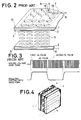
- Figure 2 of the accompanying drawings is a perspective view of a conventional ferro-electric liquid crystal cell.
- a pair of transparent glass substrates 1,1 are arranged to face each other.
- An alignment membrane 2,2 is oriented aniaxially and horizontally, and is disposed on an inner flat surface of the substrate 1,1.
- a rubbed film of polyimide, for example, is used for each of the alignment membranes. The rubbing direction of the pair of alignment membranes is substantially parallel.
- Reference numeral 3 represents a ferro-electric liquid crystal material such as a chiral smectic liquid crystal material (which will hereinafter be referred to as "SmC* material").
- the liquid crystal material has spontaneous polarization in a direction orthogonal to the major axis of the liquid crystal molecule (hereinafter referred to as the "molecular axis").
- those liquid crystal materials which have negative dielectric anisotropy ⁇ above at least a predetermined frequency are particularly useful.
- ⁇ below 0 ( ⁇ ⁇ 0) means that dielectric polarization occurs in a direction orthogonal to the molecular axis due to an external electric field having a predetermined frequency range.
- the molecules of SmC* material 3 are sandwiched between the substrates 1,1 exhibit horizontal alignment due to the influence of the alignment membranes 2,2 as shown in Figure 2 and form a layer.
- a pair of electrodes 4,5 are arranged to face each other in order to clamp the SmC* material 3 between them and to apply a driving voltage thereto.
- FIG 3 is a driving waveform diagram of a conventional liquid crystal cell.
- a first DC pulse having positive polarity is applied between the electrodes 4,5.
- the electrode 4 is kept at ground potential.
- the liquid crystal molecules are aligned in such a fashion that spontaneous polarization 6 of each liquid crystal molecule is arranged perpendicular to the electrode 4 (see Figure 2).
- This is a first stable state 7, in which the molecular axis is inclined by + ⁇ with respect to a normal 8 to the layer of SmC* material.
- dielectric polarization occurs in a direction perpendicular to the molecular long axis because the liquid crystal molecule has negative dielectric anisotropy, and the first stable state is maintained and fixed by dielectric torque.
- reference numeral 10,10 represents a pair of polarizers whose polarization axes cross each other at right angles. They clamp the SmC* material 3 and optically discriminate between the liquid crystal domains in the second stable state by utilizing birefringence.
- the first stable state is discriminated as a light cut-off state (hereinafter referred to as "black”) and the second stable state, as a light transmission state (hereinafter referred to as "white").
- the electrode arrangement of the liquid crystal cell is of a matrix structure type such as shown in Figure 4 and the scanning or segment electrodes 4 and the signal or common electrodes 5 are opposed.
- this reference does not disclose a driving waveform and a driving circuit for actually effecting line sequential driving. It is not possible to effect matrix driving using the waveform shown in Figure 3.
- the present invention seeks to provide a ferro-electric liquid crystal electro-optical device which has a drive circuit for matrix-driving, which uses spontaneous polarization of a ferro-electric liquid crystal material and its negative dielectric anisotropy, and which can write both white and black by one line sequential scanning.
- a ferro-electric liquid crystal electro-optical device which uses switching between bi-stable of ferro-electric liquid crystal molecules, including driving means for changing the states of the molecules between stable states by applying a selected signal having first and second portions, entirely of respective opposite polarities, one of the first and second portions consisting of a DC pulse of a polarity to change the state of the molecules from one to another state, and the other of the first and second portions consisting of a chopped pulse of opposite polarity ineffective to change the stable state of the molecules, the chopped pulse having a high frequency under which the ferro-electric liquid crystal molecules exhibit negative dielectric anisotropy.
- the invention also provides a method of operating a ferro-electric liquid crystal electro-optical device, including the steps of changing the state of the liquid crystal molecules by applying a selected signal having first and second portions, entirely of respective opposite polarities, one of the first and second portions consisting of a DC pulse of a polarity to change the state of the molecules from one to another stable state, and the other of the first and second portions consisting of a chopped pulse of opposite polarity ineffective to change the stable state of the molecules, the chopped pulse having a high frequency under which the ferro-electric liquid crystal molecules exhibit negative dielectric anisotropy.
- the invention also extends to a method of operating a ferro-electric liquid crystal electro-optical device of dot-matrix form, comprising a plurality of segment electrodes and a plurality of common electrodes defining a plurality of display pixels characterised in that in operation, a non-selection alternating voltage of high frequency under which the liquid crystal molecules exhibit negative dielectric anisotropy is applied to the common electrodes other than a selected common electrode a selection signal having first and second portions is applied to the selected common electrode the portions comprising DC pulses of opposite polarity and of an amplitude to change the state of the liquid crystal molecules between stable states, and signal pulses are applied to the segment electrodes each having first and second portions, corresponding in time to the first and second portions of the selection signal, one portion being a chopped pulse of the same high frequency and the other portion having zero level potential, the switching DC pulse being concurrent with the zero level potential portion, whereby a selected voltage effecting either one or the other of the stable states is applied to the display pixels on the selected common electrode.
- the present invention produces an impressed voltage for producing each stable state by the combination of a chopped pulse to which the liquid crystal molecules are not responsive and a DC pulse to which they are responsive, and arranges these DC pulses so that their phases do not overlap with each other between the impressed voltage for producing the first stable state and the impressed voltage for producing the second stable state. Therefore, when line sequential driving is carried out in a ferro-electric liquid crystal electro-optical device having a matrix electrode arrangement, the first stable state and the second stable state can be written simultaneously into each matrix pixel by one line sequential scanning operation.
- Figure 1(C) shows a matrix electrode construction of a liquid crystal cell.
- Two scanning or segment electrodes S1, S2 and two signal or common electrodes C1, C2 are arranged in such a manner as to form four matrix pixels (hereinafter referred to as "dots") D1 to D4.
- the rest of the construction of the liquid crystal cell is the same as shown in Figures 2 and 4.
- Figure 1(A) shows the waveform applied to each dot.
- This example shows the waveform for selecting the common electrode C1 by line sequential scanning and for writing simultaneously white and black to the dots D1 and D2 on the common electrode C1.
- a waveform which keeps the previous state is applied to the dots D3 and D4 on the non-selected common electrode C2
- a chopped positive pulse is applied to the dot D1 in a first half period of the selected period and a negative DC pulse in a second half period.
- the molecules of SmC* material do not respond to the chopped pulses but do to the negative DC pulses so that white (second stable state) is written into the dot D1.
- a positive DC pulse is applied to the dot D2 in the first half period of the selection period and a negative chopped pulse in the second half period.
- the molecules of SmC* material respond to the positive DC pulse in the first half period and black (first stable state) is written into the dot D2. They do not respond to the chopped pulse in the second half period.
- the selection period is divided into two half periods so that the first and second half periods are utilized for writing black and white on a time division basis, respectively, and white and black are written simultaneously by one scanning operation.
- the invention utilizes the phenomenon that molecules of the SmC* material do not respond to the chopped pulse, and the explanation of this phenomenon will be given below.
- the AC pulses applied to the unselected dots D3 and D4 and the state already written into the dots D3 and D4 is maintained by the dielectric torque based upon ⁇ ⁇ 0.
- Figure 1(B) shows the waveforms applied to the segment and common electrodes in order to generate the driving waveforms to be applied to the dots D1 to D4 shown in Figure 1(A).
- Waveform (a) represents a common selection signal applied to the common electrode C1
- waveform (b) is a common non-selection signal applied to the common electrode C2
- waveform (c) is a white write signal applied to the segment electrode S1
- waveform (d) is a black write signal applied to the segment electrode S2.
- a circuit for generating these common and segment signals will be described below.
- Waveform (a) consists of DC pulses having a positive polarity and a peak value +V and DC pulses having a negative polarity and a peak value -V with a selection period (3 msec). The display state changes from black to white.
- Waveform (b) consists of chopped pulses having a peak value of +2V in the first half of the selection period and chopped pulses having a peak value -2V in the second half.
- Figure 6 is a diagram obtained by examining the contrast ratio when black changes to white during the selection period at each voltage level while the waveforms (a) and (b) are applied with a varying voltage V.
- a large contrast ratio can be obtained at about 30 V or more.
- the molecules of SmC* material shift completely from the first stable state to the second stable state at a threshold value of at least 30 V.
- the change of the contrast is small even when a pulse having an amplitude of 60 V is applied, and it will be appreciated that molecules of the SmC* material do not completely shift from the first stable state to th second stable state.
- the properties contributing to the reversion mechanism of the molecules of the SmC* material are believed to be spontaneous polarization and dielectric torque.
- the spontaneous polarization torque always acts in such a fashion that the spontaneous polarization is in parallel with the direction of electric field, irrespective of the polarity of ⁇ .
- the dielectric torque act in such a fashion that the long axis of molecules are perpendicular to the electric field in the case of SmC* material having ⁇ ⁇ 0.
- the spontaneous polarization torque which acts in such a fashion that at the initial state where the molecules are about to shift from the first stable state to the second stable state, the long axis of molecules is in parallel with the electric field
- the dielectric torque acts in opposite directions to each other. Therefore, where ⁇ ⁇ 0, response is believed to be slower than where ⁇ > 0.
- This dielectric torque is proportional to an effective voltage (rms value of voltage).
- the effective voltage of the chopped pulse is 2 V1 while that of the DC pulse is V1 and the former is greater by a factor of 2 than the latter and acts more strongly by a factor of 2 than the latter. Therefore, response of the chopped pulse is slower than that of the DC pulse and when measurement is made with a predetermined pulse width such as shown in Figure 6, the molecules cannot completely shift from the first stable state to the second stable state and hence, the contrast ratio remains small.
- the SmC* material used for measurement was Type 3234 of Merck Co having ⁇ of -2.4.
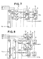
- Figure 7 shows a common (or strobe) electrode driving circuit for generating the common selection signal (waveform (a)) and the common non-selection signal (waveform (b)) shown in Fig 1(B).
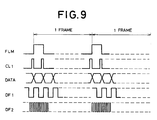
- the necessary voltage levels are +V1 and -V1 and the necessary signals for generating the AC pulses at a signal DF1 for halving the selection period into the first half and the second half and a signal DF2 for generating the necessary high frequency for holding the stable state (see the time chart of Figure 9).
- the signal DF2 is also used for chopping.
- the drive circuit of Figure 7 comprises a shift register 11, which receives a signal FLM for designating the selection period and a common shift clock CL1 for distributing line-sequentially the signal FLM to each common electrode.
- the output of the shift register 11 is connected to a gate group 12.
- the gate group 12 receives the signals DF1 and DF2 and its output controls transmission gates 13 and 14.
- the input of each transmission gate 13 is at +V1 potential and its output is applied to a respective common electrode C1, C2.
- the input of each transmission gate 14 is at -V1 potential, and its output is applied to respective common electrode C1, C2.
- the gate group 12 When the output of the shift register 12 is HIGH, the gate group 12 receives the signal DF1 and renders the transmission gates 13 conductive in the first half period and the transmission gate 14 conductive in the second half period. As a result, the common selection signal represented by waveform (a) in Figure 1(B) appears at the output of the common electrode C1. When the output of the shift register 12 is LOW, on the other hand, the gate group 12 receives the signal DF2 and outputs the AC pulse oscillating between +V1 and -V1 in synchronism with the signal DF2 to the common electrode C2. This is the common non-selection signal represented by waveform (b) in Figure 1(B).
- Figure 8 shows a signal drive circuit for generating the white write pulses (waveform (c)) and the black write pulses (waveform (d)) to be applied to the segment electrodes S1, S2.
- the signals for ON-OFF control of each transmission gate are the signals DF1 and DF2.
- a shift register 19 receives a serial video data DATA which is read and stored by a high speed clock CL2.
- a latch circuit 20 latches the video data paralleled by the shift register 19, in synchronism with the clock CL1, and outputs white or black information in accordance with the line sequential timing (clock CL1).
- a gate 21 controlled by the output of the latch circuit 20, receives the signals DF1 and DF2 as the input signal and produces the output which makes ON-OFF control to each transmission gate. As described already, the output of each transmission gate is applied to each segment electrode.
- the gate 21 When data appearing at output terminal 01 of the latch circuit 20 is white (or HIGH), the gate 21 turns ON the transmission gate 17 and outputs a high frequency signal, which is obtained by alternately turning ON and OFF the transmission gate 15 and 16 by the signal DF2 and which oscillates between +V1 and -V1, to the segment electrode S1 in the first half of the selection period and turns ON the transmission gate 18 and outputs the 0 level potential in the second half of the selection period.
- the white write signal represented by waveform (c) in Figure 1(B) can be obtained at the segment electrode S1.
- the gate 21 When the data appearing at output terminal 02 of the latch circuit 20 is black (or LOW), the gate 21 similarly outputs the 0 level potential to the segment electrode S2 in the first half of the selection period and a high frequency oscillating signal between +V1 and -V1 in the second half.
- the black write signal represented by waveform (d) in Figure 1(B) can be obtained.
- Figure 10 shows an embodiment of a common (strobe) electrode drive circuit generating non-selecting pulses (waveform (b)) as shown in Figure 1(B) having a desired amplitude.
- the dielectric torque given to ferro-electric liquid crystal molecules depends on amplitude of applied voltage, applied time and dielectric anisotropy value of the liquid crystal material. Larger amplitude of applied voltage, longer applied time or larger absolute value of dielectric anisotropy generates stronger dielectric torque.
- the ⁇ varies according to the kind of SmC* material, ambient temperature etc. Therefore, in order to give necessary torque to the ferro-electric liquid crystal molecules for obtaining high contrast, it is necessary to control the amplitude of the non-selecting signal (waveform (b)).
- Vx by setting Vx to a proper value, it is possible to obtain non-selecting signal (waveform (b)) with a desired amplitude.
- a matrix electro-optical device for writing two black and white optical states by utilizing spontaneous polarization of molecules of SmC* material and their negative dielectric anisotropy divides the selection period into two halves on the time division basis for line sequential scanning and uses the first half for a first stable state and the second half for a second stable state. Therefore, according to the present invention, it is possible to rewrite the picture in one frame and to operate at a high speed. Therefore, the present invention is suitable for displaying moving pictures.
Landscapes
- Engineering & Computer Science (AREA)
- Chemical & Material Sciences (AREA)
- Crystallography & Structural Chemistry (AREA)
- Physics & Mathematics (AREA)
- Computer Hardware Design (AREA)
- General Physics & Mathematics (AREA)
- Theoretical Computer Science (AREA)
- Liquid Crystal Display Device Control (AREA)
- Liquid Crystal (AREA)
Claims (12)
- Ferroelektrische elektrooptische Flüssigkristallanordnung, bei der eine Umschaltung zwischen bistabilen Zuständen von ferroelektrischen Flüssigkristallmolekülen (3) erfolgt, mit Treibermitteln zur Änderung der Molekülzustände zwischen stabilen Zuständen (7, 9) durch Anlegen eines ausgewählten Signals mit einem ersten und einem zweiten Signalanteil, die insgesamt jeweils entgegengesetzte Polarität besitzen, einer der beiden Signalanteile aus einem DC-Impuls mit einer Polarität zur Änderung des Molekülzustandes von einem stabilen Zustand in den anderen besteht, der andere der beiden Signalanteile aus einem zerhackten Impuls mit der entgegengesetzten für eine Änderung des stabilen Molekülzustandes unwirksamen Polarität besteht und der zerhackte Impuls eine hohe Frequenz besitzt, unterhalb der die ferroelektrischen Flüssigkristallmoleküle eine negative dielektrische Anisotropie zeigen.
- Anordnung nach Anspruch 1, dadurch gekennzeichnet, daß die Treibermittel so ausgebildet sind, daß eine erste ausgewählte Spannung, die aus dem vom DC-Impuls gefolgten zerhackten Impuls besteht, zur Realisierung eines stabilen Zustandes und eine zweite ausgewählte Spannung, die aus dem vom zerhackten Impuls gefolgten DC-Impuls besteht, zur Realisierung des anderen stabilen Zustandes angelegt wird.
- Anordnung nach Anspruch 2, dadurch gekennzeichnet, daß der zerhackte Impuls und der DC-Impuls der ersten ausgewählten Spannung gegenüber dem zerhackten Impuls und dem DC-Impuls der zweiten ausgewählten Spannung entgegengesetzte Polaritäten besitzen.
- Anordnung nach Anspruch 1, 2 oder 3, dadurch gekennzeichnet, daß die Treibermittel so ausgebildet sind, daß der zerhackte Impuls die doppelte Amplitude wie der DC-Impuls besitzt.
- Anordnung nach den vorhergehenden Ansprüchen, gekennzeichnet durch eine Punktmatrixausbildung umfassend eine Vielzahl von Abtastelektroden (S1, S2) und eine Vielzahl von Signalelektroden (C1, C2), welche eine Vielzahl von Anzeigebildpunkten (D1, D2, D3, D4) definieren.
- Anordnung nach Anspruch 5, dadurch gekennzeichnet, daß im Betrieb an jeden der Anzeigebildpunkte (D1, D2) auf einer ausgewählten Abtastzeile (C1) eine ausgewählte Spannung angelegt wird, welche entweder den einen oder den anderen stabilen Zustand der Flüssigkristallmoleküle bewirkt.
- Anordnung nach Anspruch 5 oder 6, dadurch gekennzeichnet, daß die Treibermittel so ausgebildet sind, daß an jede der Anzeigebildpunkte (D3, D4) einer nicht ausgewählten Abtastzeile (C2) eine nicht auswählende hochfrequente Spannung ohne DC-Komponente angelegt wird.
- Anordnung nach Anspruch 7, dadurch gekennzeichnet, daß die Treibermittel eine gemeinsame Quelle (DF2) für die hochfrequente nicht auswählende Spannung und den zerhackten Impuls besitzen.
- Anordnung nach den Ansprüchen 5 bis 8, dadurch gekennzeichnet, daß die Treibermittel so ausgebildet sind, daß die Amplitude einer nicht auswählenden Spannung, die an jede der Anzeigebildpunkte (D3, D4) auf einer nicht ausgewählten Abtastzeile (C2) angelegt wird, geändert wird.
- Anordnung nach Anspruch 9, dadurch gekennzeichnet, daß die Treibermittel so ausgebildet sind, daß im Betrieb die Amplitude der nicht auswählenden Spannung so eingestellt wird, daß die Flüssigkristallmoleküle (3) im wesentlichen parallel zu Substraten (1) liegen, zwischen denen sie sich befinden.
- Verfahren zum Betrieb einer ferroelektrischen elektrooptischen Flüssigkristallanordnung, bei dem die Zustände der Flüssigkristallmoleküle durch Anlegen eines ausgewählten Signale mit einem ersten und zweiten Signalanteil geändert werden, die insgesamt jeweils entgegengesetzte Polarität besitzen, einer der beiden Signalanteile aus einem DC-Impuls mit einer Polarität zur Änderung des Molekülzustandes von einem stabilen Zustand in den anderen besteht, der andere der beiden Signalanteile aus einem zerhackten Impuls mit der entgegengesetzten für eine Änderung des stabilen Molekülzustandes unwirksamen Polarität besteht und der zerhackte Impuls eine hohe Frequenz besitzt, unterhalb der die ferroelektroelektrischen Flüssigkristallmoleküle eine negative dielektrische Anisotropie zeigen.
- Verfahren zum Betrieb einer ferroelektrischen elektrooptischen Flüssigkristallanordnung mit Punktmatrixform umfassend eine Vielzahl von Segmentelektroden (S1, S2) und eine Vielzahl von gemeinsamen Elektroden (C1, C2), die eine Vielzahl von Anzeigebildpunkten (D1, D2, D3, D4) definieren, dadurch gekennzeichnet, daß im Betrieb eine nicht auswählende Wechselspannung hoher Frequenz, unterhalb der die Flüssigkristallmoleküle eine negative dielektrische Anisotropie zeigen, an die von einer ausgewählten gemeinsamen Elektrode (C2) verschiedenen gemeinsamen Elektroden (C2) angelegt wird, an die ausgewählte gemeinsame Elektrode (C1) ein Auswahlsignal mit einem ersten und zweiten Signalanteil angelegt wird, wobei die Signalanteile DC-Impulse entgegengesetzter Polarität und mit einer Amplitude zur Änderung des Zustandes der Flüssigkristallmoleküle zwischen stabilen Zuständen umfassen, und an die Segmentelektroden (S1, S2) Signalimpulse mit jeweils einem ersten und einem zweiten, dem ersten und zweiten Signalanteil des Auswahlsignals zeitlich entsprechenden Signalanteil angelegt werden, von denen ein Signalanteil ein zerhackter Impuls der gleichen hohen Frequenz ist und der andere Signalanteil Null-Potential besitzt und der Schalt-DC-Impuls mit dem Null-Potential-Signalanteil zusammenfällt, wodurch eine ausgewählte den einen oder anderen stabilen Zustand bewirkende Spannung an die Anzeigebildpunkte (D1, D2) auf der ausgewählten gemeinsamen Elektrode (C1) angelegt wird.
Applications Claiming Priority (2)
| Application Number | Priority Date | Filing Date | Title |
|---|---|---|---|
| JP61058594A JP2849740B2 (ja) | 1986-03-17 | 1986-03-17 | 強誘電性液晶電気光学装置 |
| JP58594/86 | 1986-03-17 |
Publications (3)
| Publication Number | Publication Date |
|---|---|
| EP0238287A2 EP0238287A2 (de) | 1987-09-23 |
| EP0238287A3 EP0238287A3 (en) | 1989-11-29 |
| EP0238287B1 true EP0238287B1 (de) | 1994-06-08 |
Family
ID=13088815
Family Applications (1)
| Application Number | Title | Priority Date | Filing Date |
|---|---|---|---|
| EP87302232A Expired - Lifetime EP0238287B1 (de) | 1986-03-17 | 1987-03-16 | Elektro-optische Vorrichtung mit ferroelektrischem Flüssigkristall |
Country Status (4)
| Country | Link |
|---|---|
| US (1) | US4793693A (de) |
| EP (1) | EP0238287B1 (de) |
| JP (1) | JP2849740B2 (de) |
| DE (1) | DE3789982T2 (de) |
Families Citing this family (11)
| Publication number | Priority date | Publication date | Assignee | Title |
|---|---|---|---|---|
| US4915477A (en) * | 1987-10-12 | 1990-04-10 | Seiko Epson Corporation | Method for driving an electro-optical device wherein erasing data stored in each pixel by providing each scan line and data line with an erasing signal |
| DE68929032T2 (de) * | 1988-03-24 | 2000-03-30 | Denso Corp., Kariya | Elektrooptische Einrichtung mit einem ferroelektrischen Flüssigkristall und Methode zu deren Herstellung |
| EP0864911A3 (de) * | 1988-03-24 | 1999-11-03 | Denso Corporation | Elektrooptische Einrichtung mit einem ferroelektrischen Flüssigkristall und Methode zu deren Herstellung |
| JP2640259B2 (ja) * | 1988-12-20 | 1997-08-13 | キヤノン株式会社 | 強誘電性液晶素子 |
| JPH02232623A (ja) * | 1989-03-07 | 1990-09-14 | Stanley Electric Co Ltd | 液晶シャッタの駆動装置 |
| US5798814A (en) * | 1990-08-28 | 1998-08-25 | Semiconductor Energy Laboratory Co., Ltd. | Method of driving a ferroelectric liquid crystal optical device |
| EP0599621B1 (de) * | 1992-11-25 | 1997-09-03 | Sharp Kabushiki Kaisha | Steuervorrichtung für ein Anzeigegerät, die die Spannungseinstellung verbessert |
| JP2806718B2 (ja) * | 1992-11-25 | 1998-09-30 | シャープ株式会社 | 表示装置の駆動方法及び駆動回路 |
| GB9309502D0 (en) * | 1993-05-08 | 1993-06-23 | Secr Defence | Addressing ferroelectric liquid crystal displays |
| US5933213A (en) * | 1995-09-26 | 1999-08-03 | Imation Corp. | Apparatus and method for imparting a succession of predetermined latent images on a strip of unexposed light sensitive film |
| GB9526270D0 (en) * | 1995-12-21 | 1996-02-21 | Secr Defence | Multiplex addressing of ferroelectric liquid crystal displays |
Family Cites Families (4)
| Publication number | Priority date | Publication date | Assignee | Title |
|---|---|---|---|---|
| AU584867B2 (en) * | 1983-12-09 | 1989-06-08 | Seiko Instruments & Electronics Ltd. | A liquid crystal display device |
| US4701026A (en) * | 1984-06-11 | 1987-10-20 | Seiko Epson Kabushiki Kaisha | Method and circuits for driving a liquid crystal display device |
| JPS61246721A (ja) * | 1985-04-25 | 1986-11-04 | Asahi Glass Co Ltd | 液晶電気光学素子の駆動法 |
| US4707078A (en) * | 1985-04-26 | 1987-11-17 | American Telephone And Telegraph Company, At&T Bell Laboratories | Ferroelectric liquid crystal devices using field-stabilized states |
-
1986
- 1986-03-17 JP JP61058594A patent/JP2849740B2/ja not_active Expired - Fee Related
-
1987
- 1987-03-02 US US07/020,694 patent/US4793693A/en not_active Expired - Lifetime
- 1987-03-16 DE DE3789982T patent/DE3789982T2/de not_active Expired - Fee Related
- 1987-03-16 EP EP87302232A patent/EP0238287B1/de not_active Expired - Lifetime
Also Published As
| Publication number | Publication date |
|---|---|
| EP0238287A3 (en) | 1989-11-29 |
| DE3789982T2 (de) | 1994-09-22 |
| JP2849740B2 (ja) | 1999-01-27 |
| EP0238287A2 (de) | 1987-09-23 |
| DE3789982D1 (de) | 1994-07-14 |
| US4793693A (en) | 1988-12-27 |
| JPS62215242A (ja) | 1987-09-21 |
Similar Documents
| Publication | Publication Date | Title |
|---|---|---|
| US5691740A (en) | Liquid crystal apparatus and driving method | |
| US4844590A (en) | Method and apparatus for driving ferroelectric liquid crystal device | |
| JPH01134346A (ja) | 強誘電性液晶表示装置及びその駆動方法並びに駆動波形発生方法 | |
| US4925277A (en) | Method and apparatus for driving optical modulation device | |
| EP0238287B1 (de) | Elektro-optische Vorrichtung mit ferroelektrischem Flüssigkristall | |
| US6094184A (en) | Driving method and driving circuit for ferroelectric liquid crystal display element | |
| WO1996035976A1 (en) | Method of driving antiferroelectric liquid crystal display and apparatus therefor | |
| US5436743A (en) | Method for driving optical modulation device | |
| US4927243A (en) | Method and apparatus for driving optical modulation device | |
| KR940010748A (ko) | 강 유전성 액정 패널의 구동 방법 | |
| JP2637517B2 (ja) | 液晶装置 | |
| US5841419A (en) | Control method for ferroelectric liquid crystal matrix display | |
| JP2673805B2 (ja) | 強誘電性液晶電気光学装置 | |
| JP2628157B2 (ja) | 強誘電性液晶電気光学装置 | |
| WO1994027275A1 (en) | Addressing ferroelectric liquid crystal displays | |
| JP2575196B2 (ja) | 表示装置の駆動法 | |
| KR100326453B1 (ko) | 강유전성액정표시장치의구동방법 | |
| JPS63259516A (ja) | マトリクス型液晶表示体駆動方法 | |
| JPS6256936A (ja) | 液晶マトリツクス表示パネルの駆動法 | |
| JPH07109457B2 (ja) | 液晶装置 | |
| JPH0279816A (ja) | アトリクス形強誘電性液晶パネルの駆動法 | |
| JPS63192021A (ja) | 強誘電性液晶電気光学装置 | |
| JPS62133426A (ja) | 液晶装置 | |
| JPH06214215A (ja) | 反強誘電性液晶ディスプレイの駆動方法 | |
| JPH07128641A (ja) | 液晶表示装置 |
Legal Events
| Date | Code | Title | Description |
|---|---|---|---|
| PUAI | Public reference made under article 153(3) epc to a published international application that has entered the european phase |
Free format text: ORIGINAL CODE: 0009012 |
|
| AK | Designated contracting states |
Kind code of ref document: A2 Designated state(s): CH DE FR GB IT LI SE |
|
| PUAL | Search report despatched |
Free format text: ORIGINAL CODE: 0009013 |
|
| AK | Designated contracting states |
Kind code of ref document: A3 Designated state(s): CH DE FR GB IT LI SE |
|
| 17P | Request for examination filed |
Effective date: 19900517 |
|
| 17Q | First examination report despatched |
Effective date: 19920826 |
|
| GRAA | (expected) grant |
Free format text: ORIGINAL CODE: 0009210 |
|
| AK | Designated contracting states |
Kind code of ref document: B1 Designated state(s): CH DE FR GB IT LI SE |
|
| PG25 | Lapsed in a contracting state [announced via postgrant information from national office to epo] |
Ref country code: LI Effective date: 19940608 Ref country code: CH Effective date: 19940608 |
|
| ITF | It: translation for a ep patent filed | ||
| REF | Corresponds to: |
Ref document number: 3789982 Country of ref document: DE Date of ref document: 19940714 |
|
| ET | Fr: translation filed | ||
| PG25 | Lapsed in a contracting state [announced via postgrant information from national office to epo] |
Ref country code: SE Effective date: 19940908 |
|
| REG | Reference to a national code |
Ref country code: CH Ref legal event code: PL |
|
| REG | Reference to a national code |
Ref country code: GB Ref legal event code: 746 Effective date: 19941129 |
|
| PLBE | No opposition filed within time limit |
Free format text: ORIGINAL CODE: 0009261 |
|
| STAA | Information on the status of an ep patent application or granted ep patent |
Free format text: STATUS: NO OPPOSITION FILED WITHIN TIME LIMIT |
|
| REG | Reference to a national code |
Ref country code: FR Ref legal event code: D6 |
|
| 26N | No opposition filed | ||
| REG | Reference to a national code |
Ref country code: FR Ref legal event code: D9 Free format text: CORRECTION |
|
| REG | Reference to a national code |
Ref country code: GB Ref legal event code: IF02 |
|
| PGFP | Annual fee paid to national office [announced via postgrant information from national office to epo] |
Ref country code: FR Payment date: 20050308 Year of fee payment: 19 |
|
| PGFP | Annual fee paid to national office [announced via postgrant information from national office to epo] |
Ref country code: DE Payment date: 20050310 Year of fee payment: 19 |
|
| PGFP | Annual fee paid to national office [announced via postgrant information from national office to epo] |
Ref country code: GB Payment date: 20050316 Year of fee payment: 19 |
|
| PG25 | Lapsed in a contracting state [announced via postgrant information from national office to epo] |
Ref country code: GB Free format text: LAPSE BECAUSE OF NON-PAYMENT OF DUE FEES Effective date: 20060316 |
|
| PGFP | Annual fee paid to national office [announced via postgrant information from national office to epo] |
Ref country code: IT Payment date: 20060331 Year of fee payment: 20 |
|
| PG25 | Lapsed in a contracting state [announced via postgrant information from national office to epo] |
Ref country code: DE Free format text: LAPSE BECAUSE OF NON-PAYMENT OF DUE FEES Effective date: 20061003 |
|
| GBPC | Gb: european patent ceased through non-payment of renewal fee |
Effective date: 20060316 |
|
| REG | Reference to a national code |
Ref country code: FR Ref legal event code: ST Effective date: 20061130 |
|
| PG25 | Lapsed in a contracting state [announced via postgrant information from national office to epo] |
Ref country code: FR Free format text: LAPSE BECAUSE OF NON-PAYMENT OF DUE FEES Effective date: 20060331 |