EP0238759A2 - Procédé pour inscrire de l'information optique - Google Patents
Procédé pour inscrire de l'information optique Download PDFInfo
- Publication number
- EP0238759A2 EP0238759A2 EP86309977A EP86309977A EP0238759A2 EP 0238759 A2 EP0238759 A2 EP 0238759A2 EP 86309977 A EP86309977 A EP 86309977A EP 86309977 A EP86309977 A EP 86309977A EP 0238759 A2 EP0238759 A2 EP 0238759A2
- Authority
- EP
- European Patent Office
- Prior art keywords
- donor
- molecules
- thin film
- thin
- acceptor molecules
- Prior art date
- Legal status (The legal status is an assumption and is not a legal conclusion. Google has not performed a legal analysis and makes no representation as to the accuracy of the status listed.)
- Granted
Links
Images




Classifications
-
- G—PHYSICS
- G11—INFORMATION STORAGE
- G11B—INFORMATION STORAGE BASED ON RELATIVE MOVEMENT BETWEEN RECORD CARRIER AND TRANSDUCER
- G11B7/00—Recording or reproducing by optical means, e.g. recording using a thermal beam of optical radiation by modifying optical properties or the physical structure, reproducing using an optical beam at lower power by sensing optical properties; Record carriers therefor
- G11B7/004—Recording, reproducing or erasing methods; Read, write or erase circuits therefor
- G11B7/0045—Recording
-
- G—PHYSICS
- G11—INFORMATION STORAGE
- G11B—INFORMATION STORAGE BASED ON RELATIVE MOVEMENT BETWEEN RECORD CARRIER AND TRANSDUCER
- G11B7/00—Recording or reproducing by optical means, e.g. recording using a thermal beam of optical radiation by modifying optical properties or the physical structure, reproducing using an optical beam at lower power by sensing optical properties; Record carriers therefor
- G11B7/24—Record carriers characterised by shape, structure or physical properties, or by the selection of the material
- G11B7/241—Record carriers characterised by shape, structure or physical properties, or by the selection of the material characterised by the selection of the material
- G11B7/242—Record carriers characterised by shape, structure or physical properties, or by the selection of the material characterised by the selection of the material of recording layers
- G11B7/244—Record carriers characterised by shape, structure or physical properties, or by the selection of the material characterised by the selection of the material of recording layers comprising organic materials only
-
- G—PHYSICS
- G11—INFORMATION STORAGE
- G11B—INFORMATION STORAGE BASED ON RELATIVE MOVEMENT BETWEEN RECORD CARRIER AND TRANSDUCER
- G11B7/00—Recording or reproducing by optical means, e.g. recording using a thermal beam of optical radiation by modifying optical properties or the physical structure, reproducing using an optical beam at lower power by sensing optical properties; Record carriers therefor
- G11B7/24—Record carriers characterised by shape, structure or physical properties, or by the selection of the material
- G11B7/241—Record carriers characterised by shape, structure or physical properties, or by the selection of the material characterised by the selection of the material
- G11B7/242—Record carriers characterised by shape, structure or physical properties, or by the selection of the material characterised by the selection of the material of recording layers
- G11B7/244—Record carriers characterised by shape, structure or physical properties, or by the selection of the material characterised by the selection of the material of recording layers comprising organic materials only
- G11B7/246—Record carriers characterised by shape, structure or physical properties, or by the selection of the material characterised by the selection of the material of recording layers comprising organic materials only containing dyes
- G11B7/248—Record carriers characterised by shape, structure or physical properties, or by the selection of the material characterised by the selection of the material of recording layers comprising organic materials only containing dyes porphines; azaporphines, e.g. phthalocyanines
-
- G—PHYSICS
- G11—INFORMATION STORAGE
- G11B—INFORMATION STORAGE BASED ON RELATIVE MOVEMENT BETWEEN RECORD CARRIER AND TRANSDUCER
- G11B7/00—Recording or reproducing by optical means, e.g. recording using a thermal beam of optical radiation by modifying optical properties or the physical structure, reproducing using an optical beam at lower power by sensing optical properties; Record carriers therefor
- G11B7/24—Record carriers characterised by shape, structure or physical properties, or by the selection of the material
- G11B7/241—Record carriers characterised by shape, structure or physical properties, or by the selection of the material characterised by the selection of the material
- G11B7/252—Record carriers characterised by shape, structure or physical properties, or by the selection of the material characterised by the selection of the material of layers other than recording layers
- G11B7/253—Record carriers characterised by shape, structure or physical properties, or by the selection of the material characterised by the selection of the material of layers other than recording layers of substrates
- G11B7/2531—Record carriers characterised by shape, structure or physical properties, or by the selection of the material characterised by the selection of the material of layers other than recording layers of substrates comprising glass
Definitions
- the present invention relates to an optical recording device using an organic thin film and, more particularly, to an optical recording device which utilizes a charge transfer phenomena between donor molecules (electron donative molecules) and acceptor molecules (electron acceptive molecules) and an information writing method thereof.
- the conventional recording system has various drawbacks.
- most of the conventional optical recording systems use "heat-mode" recording media, whether organic or inorganic.
- recording is performed by utilizing the fact that a recording medium melts or evaporates due to thermal energy caused by absorbed photons.
- Information is read by detecting a difference in optical reflection or absorption intensity at a recording site.
- an optical energy density must be very high to accomplish a recording.
- a signal having a predetermined detection level is to be obtained by using an inorganic chalcogenide series recording medium, e.g., Te and its analogues
- the energy density of a recording light must be at least 3 to 100 mJ/cm 2.
- a sufficiently high recording speed cannot be obtained at a finate power of light source such as semiconductor laser diode.
- Another recording system is based on photon-mode recording such as a photochromic phenomenon utilizing a change cause by absorbed photons in the molecular structure of an organic molecule.
- photon-mode recording such as a photochromic phenomenon utilizing a change cause by absorbed photons in the molecular structure of an organic molecule.
- the characteristics of the recording site such as isomerization and bond cleavage are unstable and tend to change over time.
- Still another new optical data storage system utilizes photochemical hole-buming. Since this system utilizes tautomerism of proton transfer in an organic molecule, such as porphyrin and phthalocyanine (in rigid matrices), both the conversion efficiency and speed are low and small, and its noise level cannot be decreased unless at low temperature less than 100°K. For these reasons, a high-density recording system of 10' bitslcm 2 or higher is difficult to provide, despite great potential demand for it.
- a critical defect of the conventional optical recording device is that, once information is written, it cannot be erased to allow new information to be rewritten.
- Optical magnetic disks as erasable recording media have been developed in order to eliminate this defect. Since this system reads a magnetizing direction due to a magnetic Kerr effect as a recorded signal, however, a high S/N ratio inevitably cannot be obtained, an expensive optical system to detect the signals with high resolution is required for reading, and an expensive rare earth elements must be used in order to obtain the efficient Kerr rotation. For these reasons, this system is limited only to a special application and thus lacks versatility.
- Recent developments in understanding the structure, properties and synthesis of organic materials may realize a new functional element that uses such a well-characterized organic material.
- a technique has advanced for ordering organic molecules in condensed phases and stacking their layers with the thickness of 10 A or lower, which is represented by the Langmuir-Blodgett process (to be referred to as the LB process hereinafter), a monolayer of organic material can be easily formed and built-up as a controlled layer structure. This may allow development of a new functional element by making use of the optical and electrical properties of organic molecules in controlled state.
- Roberts et al. at Durhram University in the U.K., report a semiconductor device, such as a MIS type FET and a MIS type tight-emitting element, which uses an organic thin film of the thickness below 100 ⁇ , formed by the LB process, as an insulating film on semiconductors.
- a semiconductor device such as a MIS type FET and a MIS type tight-emitting element, which uses an organic thin film of the thickness below 100 ⁇ , formed by the LB process, as an insulating film on semiconductors.
- an organic thin film obtained by the LB process is expected to serve as an optical recording medium because of its good optical response characteristics of organic molecules and the characterized film structures, it has not yet been put into practical use.
- An optical recording medium used in the present invention is made of a thin organic film containing organic molecules, i.e., donor molecules which have a high ionization potential, and organic molecules, i.e., acceptor molecules, which have a large electron affinity.
- organic molecules i.e., donor molecules which have a high ionization potential
- acceptor molecules organic molecules, i.e., acceptor molecules, which have a large electron affinity.
- the principle of the information recording of the present invention utilizes a change in optical or electrical properties of a film at a recording site due to a charge transfer phenomenon between the donor and acceptor molecules within the thin organic film caused by absorbed photon.
- an information-writing method of an optical recording device wherein light selectively irradiates a surface of a recording medium consisted of a layered structure of donor and acceptor molecules while a voltage is applied through electrodes formed on two surfaces of the film, monolayered donor molecules are thus selectively and effectively excited to cause electron transfer to the adjacent monolayer of acceptor molecules, and a change in optical and/or electrical characteristics due to the charge transfer between both the molecules in the layered structure of the film caused thereby is recorded as information.
- AE Ip(D o ) - E A (A o )
- Ip(D o ) and E A (A o ) stand for ionization potential Ip of donor and electron affinity of acceptor.
- the stabilizing energy or absorption band shifted to longer wavelength due to the charge transfer formation is expressed as: where p is the constant representing the charge transfer ratio.
- an optical recording device which comprises a recording medium made of a thin organic film containing donor and acceptor molecules and records a change in optical characteristics caused by charge transfer between the donor and acceptor molecules, characterized in that the thin organic film contains a plurality of at least either the donor or acceptor molecules, and information writing and erasing are performed by light irradiation.
- the recording medium can have a stack-layered structure wherein, between a first thin film (monolayer of donor molecule) containing donor molecules and a second thin film (monolayer of acceptor molecule) containing acceptor molecules, a third thin film containing acceptor molecules of a type different from that of the acceptor molecules contained in the second thin film is present.
- a built-up substructure of each monolayers wherein, between a first thin film containing donor molecules and a second thin film containing acceptor molecules, a third thin film containing donor molecules of a type different from that of the donor molecules contained in the first thin film is present, is repeated to constitute a stack layer structure, thus providing a recording medium.
- Information writing is performed by irradiating light having a predetermined wavelength onto such a recording medium and changing the donor and acceptor molecules to an ionic state.
- Information erasing is performed by irradiating long-wavelength light or white light having a high intensity and returning the donor and acceptor molecules from the ionic to neutral state. An erasable recording device is thus provided.
- a thin film containing donor or acceptor molecules of a type different from that in the donor molecule film or the acceptor molecule film is provided, in order to improve the writing efficiency and to hold the ionic state, i.e., the writing condition, more stably. Since another insulating molecule film is provided between the donor and acceptor molecule films, the recording condition can be held more stably. Molecules which have changed from a neutral state to an ionic state can be returned to the neutral state by irradiating long-wavelength light or white light having a high intensity. This corresponds to the information erasing operation.
- information writing and erasing do not involve a large conformational change and a bond cleavege in a molecule. This is different from the conventional heat mode recording of or light recording of the photon mode which utilizes a change in extinction modulus or reflectance caused by the structural change of a molecule.
- High-quality information writing and erasing are thus enabled. Since a change in extinction modulus, reflectance, reflective index or the like due to the charge transfer is large, an expensive optical system is not required for light recording, an inexpensive organic material can be used as a material of the recording medium, and an inexpensive recording device can be provided. Also, when a change in extinction modulus, reflectance, refractive index or the like of the recording medium is optically read as information, reading with a high S/N ratio can be performed.
- an external electric field can be effectively used, as in the first embodiment. More specifically, when an external electric field is applied in a direction to enhance charge transfer, writing and erasing efficiency can be improved. When an external electric field is applied in a direction to interfere with charge transfer, information damage caused by repeated reading can be prevented. Furthermore, when electrodes for applying the external electric field are provided, an insulating molecule film is preferably also provided between the electrode and the thin organic film. This prevents charge transfer from the electrode to the thin organic film and improves the charge transfer efficiency between organic molecules and the holding performance of the recording condition.
- an optical recording device which comprises a thin organic film, containing donor and acceptor molecules, as a recording medium, and records a change in optical characteristics caused by charge transfer between the donor and acceptor molecules as information, wherein the optical recording device contains a plurality of types of at least either the donor or acceptor molecules, and two or more types of beams having different wavelengths are irradiated to cause charge transfer between the donor and acceptor molecules in different wavelength ranges, thereby recording information in a multiplex manner.
- charge transfer is caused between donor and acceptor molecules of a specific combination by excitation by light having a specific wavelength, and between donor and acceptor molecules of another combination by excitation by light having another wavelength.
- a light source suitable for information recording various types of gas lasers ranging from ultraviolet to range, a dye laser which is pumped by various methods, a semiconductor laser, and monochromatic light obtained by decomposing light from a white light source such as an Xe lamp, can be used.
- a light source can be arbitrarily selected as far as it corresponds to the wavelength, where the neutral state of the molecules constituting the recording medium layer have absorption bands.
- the absorption spectrum of the molecules is shifted to the long-wavelength range, molecules that exhibit absorption in the ultraviolet range in the neutral state now exhibit absorption extending to the visible range, and molecules that exhibit absorption in the visible range in the neutral state now exhibit absorption extending to the infrared range.
- the reflectivity and refractive index of the recording medium are also changed. Namely, information is recorded as a change in light transmittance or reflectivity.
- a plurality of combinations of donor and acceptor molecule films for charge transfer are provided. The respective combinations are excited by irradiating light having corresponding wavelengths, thus performing information recording in a multiplex manner.
- information can be recorded in a three-dimensional manner by, e.g., recording specific information in a specific layer with light having wavelength ⁇ l and another specific information in another specific layer with light having wavelength X2.
- high-density recording is enabled more effectively, compared to various types of conventional optical recording devices that perform information recording in a two-dimensional manner.
- Other advantages of the third embodiment are the same as those of the second embodiment described above.
- the thin organic film of the present invention is formed by the LB process.
- the thin organic film preferably has a super lattice structure having a plurality of stacked layers each consisting of donor and acceptor molecule films.
- the thickness of the donor or acceptor molecule film is preferably 5 to 500 A, and more preferably 5 to 100 A.
- a thin organic film (insulating molecule film) containing electrically inactive insulating molecules is preferably provided between the donor and acceptor molecule films.
- the insulating molecule here means an organic molecule having a small electron density of, e.g., non-localized 7 r-electron or un-paired n-electron.
- the following donor molecules can be used as the donor molecules used in the present invention.
- the present invention allows for the application of the derivatives of the donor type molecules indicated in items (1) to (7), which have a hydrophobic group with a structural formula (where n and p+q+l respectively represent larger numbers than 8), or a hydrophilic group with a structural formula of -COOH, -OH, SO 3 H, -COOR', -NH 2 , -N ⁇ (R') 3 Y - (Y denotes halogen ions), or have both said hydrophobic and hydrophilic groups.
- amine type donors are preferred, but fulvalene type donors and S-containing heterocyclic compound are more preferred.
- acceptor molecules include the following:
- the present invention allows for the application of the derivatives of the acceptor type molecules having the essential structural formula indicated in items (I) to (3), which have hydrophobic radicals represented by (where n and a total of p + q + l respectively denote a larger number than 8), or hydrophilic radicals represented by -COOH, -OH, -SO,H, -COOR', -NH 2 , -N ⁇ (R')3Y - (Y denotes halogen ions), or have both such hydrophobic and hydrophilic radicals.
- hydrophobic radicals represented by (where n and a total of p + q + l respectively denote a larger number than 8)
- hydrophilic radicals represented by -COOH, -OH, -SO,H, -COOR', -NH 2 , -N ⁇ (R')3Y - (Y denotes halogen ions), or have both such hydrophobic and hydrophilic radicals.
- quinone type donors are preferred and cyano compound type donors are more preferred.
- the above-mentioned insulating or inactive organic molecules include the undermentioned types.
- the subject polymerizable molecules may be represented, for example, by:
- the above-mentioned molecules (2) can be applied intact.
- the molecules which can not be fabricated into a film by themselves are applied when mixed with the insulating molecules (listed in item (I)) which can be independently formed into a film.
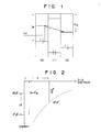
- Fig. I is an energy state diagram showing a state wherein insulating molecule film I having thickness a is provided between donor molecule film D, having an ionization potential lp, and acceptor molecule film A, having electron affinity E A .
- state D°A° wherein the respective molecules are neutral
- state D A° wherein donor molecules are selectively excited.
- state D A° part of the structure is returned to the ground state and its other part is shifted to state D + IA - , wherein charge transfer is caused.
- D + IA- indicates a state wherein donor and acceptor molecules have respectively been changed positive and negative ionic states, with insulating molecule film I sandwiched therebetween.
- the energy in state D + IA- must be lower than that in state D A°, i.e., must be satisfied.
- transition speed from state D * A° to D + IA - depends on the electron affinity and thickness of insulating molecule film 1.
- a third organic molecule film donor molecule film or acceptor molecule film
- the conversion efficiency becomes higher and more stable recording is possible.
- the process from state D 2 A° to D + IA - can be controlled by the direction and intensity of the extemal electric field. Therefore, memory damage during efficient writing and recording can be prevented by applying an extemal voltage.
- the relaxation process of the excitation undergoes a radiationless process or a fluorescence process (rate constant: Kr), to ground state G D , or a phosphorescence relaxation process (rate constant: Df), which returns to the ground state after intersystem crossing via the triplet state Eh.
- Kr fluorescence process
- Df phosphorescence relaxation process
- transition of the electron-hole pairs formed by the excitation from state Eh (rate constant: Ke) to state C r occurs at constant rate ⁇ (E), and electrons migrate to acceptor molecules nearby and holes migrate to donor molecules in the neutral state, as a result of the electric field (charge transfer state).
- This charge transfer state can be caused only by light excitation without applying an external electric field.
- relaxation quantum yield ⁇ thereof to the initial ground state (Go and G A ) occurs prior to other transitions, and the recording state is instantaneously extinguished by the following reaction scheme:
- the value of quantum yield is expressed as: when no bias is applied.
- electron-hole dissociation occurs at rate ⁇ (E), and the quantum yield for the relaxation to the initial state is thus considerably decreased as expressed as follows:
- an energy required for forming electron-hole pairs, i.e., precursors of charge transfer is about in voltage. Accordingly, in order to sufficiently increase the ratio of charge transfer and to raise the recording contrast, an organic thin film must have a very high threshold voltage of about 10 7 V/cm, which cannot be adopted from a practical point of view.
- Fig. 4 shows an arrangement of a recording medium according to a first embodiment of the present invention.
- 150- ⁇ thick NESA a transparent conductive electrode
- film 2 was formed on glass substrate I, and 500-A thick SiO 2 film 3 was formed on film 2.
- a NESA film/SiO 2 film was formed on a glass substrate, and the resultant substrate was placed in the water phase.
- the film-forming molecules were developed and the film was deposited onto the substrate at a rate of 70 ⁇ m/sec to build-up donor molecule film 4.
- insulating molecule film 5 of arachic acid was formed at a surface pressure of 25 dyne/cm, and a mixture film consisting of tetracyanoquinodimethane and stearic acid at a mixing molar ratio of I : I was formed as acceptor molecule film 6 thereon.
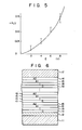
- Fig. 5 shows a result obtained by measuring the absorbance change ⁇ A CT for a wavelength of 850 nm at a recording portion by changing a bias voltage to be applied.
- the bias voltage when the bias voltage is increased, the absorption strength is considerably increased.
- a high-speed, highly efficient information recording can be performed.
- Fig. 6 shows an arrangement of a recording medium according to a second embodiment of the present invention.
- 150- ⁇ thick nesa film 12 was formed on glass substrate 11.
- a NESA (indium and tin oxide) film was formed on a glass substrate, and the resultant substrate was placed in the trough.
- the film-forming molecules were spreaded over the subphase and the film was build up at a dipping and pulling rate of 70 um/sec to form donor molecule film 13.
- insulating molecule film 14 of arachic acid was formed at a surface pressure of 25 dyne/cm, and a film consisting of the mixture of tetracyanoquinodimethane and stearic acid at a molar ratio of I : I was formed as acceptor molecule film 15.
- Acceptor molecule film 16 comprising a mixture film consisting of tetracyanoethylene and stearic acid that are acceptor molecules having a larger electron affinity than that of film 15, was formed thereon by the same procedures as described above. These operations were sequentially repeated a plurality of times to build up ten donor molecule films 13, insulating molecule films 14, and acceptor molecule films 15 and 16, respectively. The resultant structure was set in a vacuum deposition system to deposit Au electrode 17 in a vacuum of 3 x 10- 6 Torr.
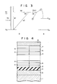
- Fig. 7 is an energy state diagram of a unit stack layer structure of a recording medium having the arrangement as described above.
- light having a predetermined wavelength is irradiated to excite donor molecule film D
- electrons formed therein migrate from insulating molecule film I to acceptor molecule film A 2 through acceptor molecule film A, and are set in an ionic state. This corresponds to a writing state. Since films I and A, are provided between film D and A z , the recording condition can be stably held and efficient writing can be performed.
- Fig. 8 shows a result obtained by measuring absorption strength ⁇ A CT for a wavelength 850 nm at a recording portion by changing a bias voltage to be applied.
- the absorption strength was measured at light output of 10 ⁇ W/mm 2 .
- the bias voltage is increased, the absorption strength is considerably increased.
- efficient information recording can be performed.
- the holding characteristics of information recorded as a difference in the light absorption characteristics in this manner were stable, and were not changed even when the recording medium was left to stand in air for a month.
- the absorption strength for a wavelength of 850 nm was decreased to 0.005.
- Fig. 9 shows the result of this experiment. It is seen from Fig. 9 that when reading is performed while applying a voltage exceeding 3 V, substantially no destruction occurs in the storage contents by a reading operation.
- a reversible information recording device capable of recording and erasing information by light irradiation can be obtained.
- this recording device a change in the light absorption rate which occurs as a result of the charge transfer phenomenon is significant. Therefore, this recording device does not require an expensive optical system.
- the recording medium of the recording device contains inexpensive organic molecules, the device has a good S/N ratio and excellent versatility. Between donor and acceptor molecules in the layered structure of films, which perform charge transfer, an acceptor molecule film using different acceptor molecules is provided, together with an insulating molecule film. Therefore, a recording device having a good writing efficiency and stable holding characteristics for recording conditions can be obtained. In particular, when an appropriate bias voltage is applied upon writing, erasing, and reading, more efficient writing/erasing characteristics and more stable holding characteristics for recording conditions can be obtained.
- Figs. 10 to 12 show arrangements of unit organic thin film stack layer structures according to other embodiments in correspondence with the energy state diagram of Fig. 7 of the embodiment described above.
- Fig. 10 shows a case wherein two types of donor molecule films and one type of acceptor molecule film are used. More specifically, between donor molecule film D, and acceptor molecule film A, donor molecule film D Z , which has ionization potential I p2 higher than ionization potential I pl , of film D 1 , is provided together with insulating molecule film I. With this stack layer structure, efficient writing and erasing characteristics, and stable characteristics for holding recording conditions can be obtained in accordance with the same principle as the embodiment described above.
- Fig. II shows a case wherein the insulating molecule film shown in Fig. 10 is omitted and two types of donor molecule films D, and D 2 and acceptor molecule film A are used.
- the electrons and holes migrate to film A and D,, respectively, as shown in Fig. II, thereby providing an ionic state, i.e., a writing state.
- an insulating molecule film is not used.
- the thickness and ionization potential of central film D 2 are appropriately selected, stable holding characteristics for recording conditions can be obtained.
- Fig. 12 shows a case of the same structure as Fig. II, wherein information can be written by optically exciting acceptor molecule film A.
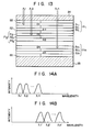
- Fig. 13 schematically shows an arrangement of an information recording medium according to a third embodiment of the present invention.
- Reference numeral 23 denotes a substrate, e.g., a glass substrate having a nesa film formed thereon.
- a super lattice film is formed on substrate 23 by the LB process, and electrode 24 is formed thereon. More specifically, the super lattice film is formed by stacking first, second,... and nth recording layers 21,, 21 2 ,... and 21 n through insulating molecule films 22.
- First layer 21, is formed by stacking donor molecule film 31,, containing first donor molecules D,, and acceptor molecule film 33 1 , containing first acceptor molecules A,, through insulating film 32,.
- Second layer 21 2 is formed by stacking donor molecule film 31 2 , containing second donor molecules D z , and acceptor molecule film 33 2 , containing second acceptor molecules A Z , through insulating film 32 2 . In this manner, a plurality of recording layers, having different light absorption characteristics by different combinations of donor and acceptor molecule films, are stacked.
- Figs. 14A and 14B show light absorption characteristics of this recording medium.
- Fig. 14A shows the characteristics of the recording medium in which no information has been recorded.
- the absorption peak of wavelength ⁇ l corresponds to the donor molecule film first layer 21,, that of wavelength ⁇ 2 corresponds to the donor molecule film of second layer 21 2 ,... and that of wavelength ⁇ n corresponds to the donor molecule film of nth layer 21 n .
- information is written in the recording medium having such absorption characteristics by using light having wavelength ⁇ l.
- charge transfer occurs between donor and acceptor molecule films 31, and 33, of first layer 21, where light irradiates, and the ionization state at this portion is held.
- a predetermined external electric field may be applied to the recording medium. This is effective since it promotes dissociation of electron-hole pairs formed by light excitation.
- the insulating molecule film in each recording layer serves to increase the writing efficiency and to hold the recording conditions.
- Fig. 15 shows an example of a practical information writing system.
- Reference numeral 35 denotes an incandescent light source; 36, a scan control system of light source 35; 37, a mirror; 38, a filter; and 39, a focusing lens.
- a wavelength is selected by filter 38 and information writing is performed in a predetermined recording layer of the recording medium in the above manner by using light having a predetermined wavelength. In this manner, information can be written in a recording medium in a three-dimensional manner and in a multiplex manner by using a plurality of wavelengths.
- Fig. 16 schematically shows a case wherein information is read from a recording medium in which information is written.
- a2 ... respectively denote information recording units of first recording layer 21,
- information recording of a higher density can be performed, compared to those of the conventional heat mode method.
- Information is optically read using wavelengths ⁇ l', ⁇ 2',..., and Xn' in Fig. 14B as reading wavelengths. More specifically, when the light source for light having wavelength ⁇ 1' is scan-controlled and a light absorption strength distribution by the recording medium is measured, information in first layer 21, can be read out. Similarly, when light having wavelength X2' is scanned, information in second layer 21 2 can be read out.
- Fig. 17 schematically shows an arrangement of a system for reading out information in this manner.
- the system of Fig. 17 is basically the saine as that of Fig. 15. Reading wavelengths are sequentially selected by filter 40 in the order of hi', ⁇ 2',..., and ⁇ n' and absorption strength distributions in the recording medium with the respective wavelengths are measured. Multiplex information can be read out in this manner.
- light transmitted through the recording medium is detected by photodetector 14.
- the substrate is designed as a reflecting substrate, light reflected by the substrate can be read out.
- a recording device wherein information is recorded in a considerably high density by using light having a plurality of wavelengths, can be obtained. Furthermore, since the information recording principle of the present invention utilizes charge transfer between molecules by the photon mode, when writing is performed using an external electric field as well, high-sensitive, high-contrast information recording can be performed.
- the present invention is not limited to the above embodiments.
- either the donor or acceptor molecule films of first, second,... recording layers 21" 21 Z ,... can be the same.
- An appropriate acceptor or donor molecule film can be provided in place of an insulating molecule film between the donor and acceptor molecule films of each recording layer. More specifically, between a first organic thin film containing donor molecules and a second organic thin film containing acceptor molecules, a third organic thin film containing acceptor molecules having a smaller electron affinity than that of the second organic thin film, or a third organic thin film containing donor molecules having a larger electron affinity than that of the first organic thin film, can be provided.
- the combination of different donor and acceptor molecule films need not be stacked as different layers, but can be an appropriate mixture film.
Landscapes
- Optical Record Carriers And Manufacture Thereof (AREA)
- Non-Silver Salt Photosensitive Materials And Non-Silver Salt Photography (AREA)
- Optical Recording Or Reproduction (AREA)
Applications Claiming Priority (6)
| Application Number | Priority Date | Filing Date | Title |
|---|---|---|---|
| JP66276/86 | 1986-03-25 | ||
| JP61066276A JPS62221593A (ja) | 1986-03-25 | 1986-03-25 | 光学的情報記録装置の情報書込み方法 |
| JP61129689A JPS62284785A (ja) | 1986-06-04 | 1986-06-04 | 光学的情報記録装置 |
| JP129692/86 | 1986-06-04 | ||
| JP129689/86 | 1986-06-04 | ||
| JP61129692A JP2509566B2 (ja) | 1986-06-04 | 1986-06-04 | 光学的情報記録装置 |
Publications (3)
| Publication Number | Publication Date |
|---|---|
| EP0238759A2 true EP0238759A2 (fr) | 1987-09-30 |
| EP0238759A3 EP0238759A3 (en) | 1989-02-08 |
| EP0238759B1 EP0238759B1 (fr) | 1992-03-11 |
Family
ID=27299076
Family Applications (1)
| Application Number | Title | Priority Date | Filing Date |
|---|---|---|---|
| EP86309977A Expired EP0238759B1 (fr) | 1986-03-25 | 1986-12-19 | Procédé pour inscrire de l'information optique |
Country Status (3)
| Country | Link |
|---|---|
| US (1) | US4819210A (fr) |
| EP (1) | EP0238759B1 (fr) |
| DE (1) | DE3684306D1 (fr) |
Cited By (7)
| Publication number | Priority date | Publication date | Assignee | Title |
|---|---|---|---|---|
| EP0407005A1 (fr) * | 1989-06-10 | 1991-01-09 | THORN EMI plc | Dispositif de vÀ©rification pour un système de sécurité |
| EP0363147A3 (fr) * | 1988-10-04 | 1991-07-17 | Canon Kabushiki Kaisha | Appareil et procédé d'enregistrement et de reproduction et milieu d'enregistrement pour le procédé d'enregistrement et de reproduction |
| EP0331477A3 (fr) * | 1988-03-02 | 1991-10-02 | Kabushiki Kaisha Toshiba | Film mince de colorant organique et élément en film mince organique |
| EP0820057A1 (fr) * | 1996-07-18 | 1998-01-21 | Fuji Photo Film Co., Ltd. | Médium pour l'enregistrement d'informations |
| EP0822544A1 (fr) * | 1996-07-29 | 1998-02-04 | Mitsui Toatsu Chemicals, Incorporated | Médium d'enregistrement optique |
| US6203876B1 (en) * | 1996-07-18 | 2001-03-20 | Fuji Photo Film Co., Ltd. | Information recording medium |
| CN112309440A (zh) * | 2020-10-21 | 2021-02-02 | 西北工业大学 | 基于铂-二维硒化铟-少层石墨肖特基二极管的光存储器件及存储方法 |
Families Citing this family (20)
| Publication number | Priority date | Publication date | Assignee | Title |
|---|---|---|---|---|
| US4907195A (en) * | 1984-09-14 | 1990-03-06 | Xerox Corporation | Method of and system for atomic scale recording of information |
| DE3790965T1 (de) * | 1987-06-10 | 1989-07-06 | Mitsubishi Electric Corp | Optisches aufzeichnungsmaterial |
| US5301145A (en) * | 1987-07-13 | 1994-04-05 | Sharp Kabushiki Kaisha | Method and apparatus for recording and reading information, and an information recording element |
| US5107483A (en) * | 1987-08-19 | 1992-04-21 | Mitsubishi Denki Kabushiki Kaisha | Frequency selective optical data record/regenerate apparatus |
| JP2671139B2 (ja) * | 1987-12-10 | 1997-10-29 | 富士写真フイルム株式会社 | 情報記録媒体,光情報記録方法および光情報記録再生方法 |
| US5024927A (en) * | 1988-10-06 | 1991-06-18 | Ricoh Company, Ltd. | Information recording medium |
| DE69011167T2 (de) * | 1989-03-31 | 1994-12-22 | Toshiba Kawasaki Kk | Anzeigeelement mit organischem Dünnschichtfilm. |
| EP0396943B1 (fr) * | 1989-04-18 | 1995-07-05 | Nippon Telegraph And Telephone Corporation | Milieu de mémoire optique et procédé de mémorisation |
| US5264876A (en) * | 1989-08-10 | 1993-11-23 | Canon Kabushiki Kaisha | Recording medium, method for preparing the same, recording and reproducing device, and recording, reproducing and erasing method by use of such recording medium |
| US5195082A (en) * | 1989-12-12 | 1993-03-16 | Optex Corporation | Optical disk structures for electron trapping optical memory media |
| US4999809A (en) * | 1990-03-09 | 1991-03-12 | Eastman Kodak Company | Photorefractive device and process for its use |
| US5182669A (en) * | 1990-06-04 | 1993-01-26 | Pioneer Electronic Corporation | High density optical disk and method of making |
| JP3150331B2 (ja) * | 1990-09-28 | 2001-03-26 | 株式会社東芝 | 有機薄膜素子 |
| US5410531A (en) * | 1991-03-28 | 1995-04-25 | Sanyo Electric Co., Ltd. | Noise reduction in a multiplex recorded optical information system |
| US5217792A (en) * | 1991-10-17 | 1993-06-08 | At&T Bell Laboratories | Stable polar optically nonlinear multilayer films and devices using the same |
| US5251198A (en) * | 1992-05-29 | 1993-10-05 | Strickler James H | Reading device for multi-layered optical information carrier |
| US5327373A (en) * | 1992-08-21 | 1994-07-05 | Board Of Regents, The University Of Texas System | Optoelectronic memories with photoconductive thin films |
| JP3477024B2 (ja) * | 1997-02-25 | 2003-12-10 | 株式会社東芝 | 記録媒体、記録方法、消去方法、再生方法、記録・再生方法、再生装置および記録・再生装置 |
| US6569705B2 (en) * | 2000-12-21 | 2003-05-27 | Intel Corporation | Metal structure for a phase-change memory device |
| DE10126578C2 (de) * | 2001-05-31 | 2003-06-18 | Infineon Technologies Ag | Verwendung von Molekül- bzw. Polymerschichten als Speicherelemente |
Family Cites Families (15)
| Publication number | Priority date | Publication date | Assignee | Title |
|---|---|---|---|---|
| US3801966A (en) * | 1971-08-18 | 1974-04-02 | Hitachi Ltd | Optical memory device |
| FR2266197A1 (en) * | 1974-03-25 | 1975-10-24 | Xerox Corp | Photoconducting material for electrophotographic image plates - consisting of homogeneous solid soln. of photogenerator in insulating polymer matrix |
| US3932025A (en) * | 1974-10-25 | 1976-01-13 | Xerox Corporation | Imaging system |
| US4101976A (en) * | 1977-02-14 | 1978-07-18 | International Business Machines Corporation | Frequency selective optical data storage system |
| US4394749A (en) * | 1979-06-08 | 1983-07-19 | Hitachi, Ltd. | Photoelectric device and method of producing the same |
| US4538252A (en) * | 1981-08-24 | 1985-08-27 | International Business Machines Corporation | Light induced capacitance changes in donor polymers (or small molecules) films and its use for information storage in video disks and the like |
| US4534015A (en) * | 1981-10-05 | 1985-08-06 | Qmc Industrial Research Limited | Information holding device |
| JPS58209594A (ja) * | 1982-05-31 | 1983-12-06 | Nippon Telegr & Teleph Corp <Ntt> | 光学的記録媒体 |
| US4574366A (en) * | 1983-02-07 | 1986-03-04 | The Johns Hopkins University | Optical storage and switching devices using organic charge transfer salts |
| GB2142494A (en) * | 1983-05-20 | 1985-01-16 | Rikagaku Kenkyusho | Methods of recording information in and reading information from a ferroelectric polymer material |
| NL8301956A (nl) * | 1983-06-02 | 1985-01-02 | Optical Storage Int | Optisch registratie element. |
| US4566086A (en) * | 1983-06-13 | 1986-01-21 | Ncr Corporation | Information storage system utilizing electrets |
| JPS60160036A (ja) * | 1984-01-28 | 1985-08-21 | Toshiba Corp | 光デイスク |
| US4663270A (en) * | 1984-04-25 | 1987-05-05 | The Johns Hopkins University | Multistate optical switching and memory using an amphoteric organic charge transfer material |
| JPH0671828B2 (ja) * | 1985-01-25 | 1994-09-14 | 株式会社日立製作所 | 情報記録用薄膜 |
-
1986
- 1986-12-19 EP EP86309977A patent/EP0238759B1/fr not_active Expired
- 1986-12-19 DE DE8686309977T patent/DE3684306D1/de not_active Expired - Lifetime
-
1988
- 1988-06-06 US US07/205,542 patent/US4819210A/en not_active Expired - Lifetime
Cited By (13)
| Publication number | Priority date | Publication date | Assignee | Title |
|---|---|---|---|---|
| EP0331477A3 (fr) * | 1988-03-02 | 1991-10-02 | Kabushiki Kaisha Toshiba | Film mince de colorant organique et élément en film mince organique |
| US5153680A (en) * | 1988-03-02 | 1992-10-06 | Kabushiki Kaisha Toshiba | Organic dye thin film and organic thin film element |
| EP0363147A3 (fr) * | 1988-10-04 | 1991-07-17 | Canon Kabushiki Kaisha | Appareil et procédé d'enregistrement et de reproduction et milieu d'enregistrement pour le procédé d'enregistrement et de reproduction |
| US5439777A (en) * | 1988-10-04 | 1995-08-08 | Canon Kabushiki Kaisha | Recording and reproducing apparatus and method for applying a pulse voltage and an electromagnetic wave |
| EP0407005A1 (fr) * | 1989-06-10 | 1991-01-09 | THORN EMI plc | Dispositif de vÀ©rification pour un système de sécurité |
| US6203876B1 (en) * | 1996-07-18 | 2001-03-20 | Fuji Photo Film Co., Ltd. | Information recording medium |
| EP0820057A1 (fr) * | 1996-07-18 | 1998-01-21 | Fuji Photo Film Co., Ltd. | Médium pour l'enregistrement d'informations |
| US5879772A (en) * | 1996-07-18 | 1999-03-09 | Fuji Photo Film Co., Ltd. | Information recording medium |
| EP0822544A1 (fr) * | 1996-07-29 | 1998-02-04 | Mitsui Toatsu Chemicals, Incorporated | Médium d'enregistrement optique |
| US6060606A (en) * | 1996-07-29 | 2000-05-09 | Mitsui Chemicals, Inc. | Dipyrromethene metal chelate compounds |
| US5948593A (en) * | 1996-07-29 | 1999-09-07 | Mitsui Chemicals, Inc. | Optical recording medium |
| CN112309440A (zh) * | 2020-10-21 | 2021-02-02 | 西北工业大学 | 基于铂-二维硒化铟-少层石墨肖特基二极管的光存储器件及存储方法 |
| CN112309440B (zh) * | 2020-10-21 | 2022-04-26 | 西北工业大学 | 基于铂-二维硒化铟-少层石墨肖特基二极管的光存储器件及存储方法 |
Also Published As
| Publication number | Publication date |
|---|---|
| US4819210A (en) | 1989-04-04 |
| EP0238759B1 (fr) | 1992-03-11 |
| DE3684306D1 (de) | 1992-04-16 |
| EP0238759A3 (en) | 1989-02-08 |
Similar Documents
| Publication | Publication Date | Title |
|---|---|---|
| EP0238759B1 (fr) | Procédé pour inscrire de l'information optique | |
| Dvornikov et al. | Two-photon three-dimensional optical storage memory | |
| US6280904B1 (en) | Photo-chemical generation of stable fluorescent derivatives of rhodamine B | |
| EP0218263B1 (fr) | Milieu d'enregistrement d'informations laser ayant une couche d'enregistrement | |
| Kuhn et al. | Monolayer assemblies | |
| JP4372048B2 (ja) | 屈折率変化素子 | |
| KR101098700B1 (ko) | 정보 기록 매체 및 그 제조 방법, 및 기록 재생 방법, 광학정보 기록 재생 장치 | |
| US6807138B1 (en) | Light drive | |
| Dvornikov et al. | Materials and systems for two photon 3-D ROM devices | |
| EP0396943B1 (fr) | Milieu de mémoire optique et procédé de mémorisation | |
| Żmija et al. | New organic photochromic materials and selected applications | |
| KR920006313B1 (ko) | 광정보기록매체 및 광기록방법 | |
| JP2509566B2 (ja) | 光学的情報記録装置 | |
| Barachevsky | Organic frequency: selective recording media | |
| Zhao et al. | Dynamic studies on laser-induced gratings in azobenzene-doped polymer film | |
| Zhang et al. | Diarylethene materials for photon-mode optical storage | |
| Nagamura et al. | Transient and Steady Photoelectric Responses of LB Films Containing Amphipathic Porphyrin and Redox Chromophores | |
| JPS62221593A (ja) | 光学的情報記録装置の情報書込み方法 | |
| JP2577633B2 (ja) | 光学記憶媒体 | |
| Ford et al. | Three-dimensional two-photon memory materials and systems | |
| KR20060036913A (ko) | 광 기록매체 | |
| JPS61117537A (ja) | 光記録媒体 | |
| JPH0443572B2 (fr) | ||
| Moerner | Laser light-induced physical processes in optical materials: Persistent spectral hole-burning | |
| JPH05139040A (ja) | Phb光記録媒体 |
Legal Events
| Date | Code | Title | Description |
|---|---|---|---|
| PUAI | Public reference made under article 153(3) epc to a published international application that has entered the european phase |
Free format text: ORIGINAL CODE: 0009012 |
|
| AK | Designated contracting states |
Kind code of ref document: A2 Designated state(s): DE FR GB NL |
|
| 17P | Request for examination filed |
Effective date: 19880204 |
|
| PUAL | Search report despatched |
Free format text: ORIGINAL CODE: 0009013 |
|
| AK | Designated contracting states |
Kind code of ref document: A3 Designated state(s): DE FR GB NL |
|
| 17Q | First examination report despatched |
Effective date: 19900824 |
|
| GRAA | (expected) grant |
Free format text: ORIGINAL CODE: 0009210 |
|
| AK | Designated contracting states |
Kind code of ref document: B1 Designated state(s): DE FR GB NL |
|
| PG25 | Lapsed in a contracting state [announced via postgrant information from national office to epo] |
Ref country code: NL Effective date: 19920311 |
|
| REF | Corresponds to: |
Ref document number: 3684306 Country of ref document: DE Date of ref document: 19920416 |
|
| ET | Fr: translation filed | ||
| NLV1 | Nl: lapsed or annulled due to failure to fulfill the requirements of art. 29p and 29m of the patents act | ||
| PLBE | No opposition filed within time limit |
Free format text: ORIGINAL CODE: 0009261 |
|
| STAA | Information on the status of an ep patent application or granted ep patent |
Free format text: STATUS: NO OPPOSITION FILED WITHIN TIME LIMIT |
|
| 26N | No opposition filed | ||
| REG | Reference to a national code |
Ref country code: GB Ref legal event code: IF02 |
|
| PGFP | Annual fee paid to national office [announced via postgrant information from national office to epo] |
Ref country code: FR Payment date: 20051208 Year of fee payment: 20 |
|
| PGFP | Annual fee paid to national office [announced via postgrant information from national office to epo] |
Ref country code: GB Payment date: 20051214 Year of fee payment: 20 |
|
| PGFP | Annual fee paid to national office [announced via postgrant information from national office to epo] |
Ref country code: DE Payment date: 20051215 Year of fee payment: 20 |
|
| PG25 | Lapsed in a contracting state [announced via postgrant information from national office to epo] |
Ref country code: GB Free format text: LAPSE BECAUSE OF EXPIRATION OF PROTECTION Effective date: 20061218 |
|
| REG | Reference to a national code |
Ref country code: GB Ref legal event code: PE20 |