EP0240070A2 - Procédé pour la fabrication de dispositifs à semi-conducteur - Google Patents
Procédé pour la fabrication de dispositifs à semi-conducteur Download PDFInfo
- Publication number
- EP0240070A2 EP0240070A2 EP87200532A EP87200532A EP0240070A2 EP 0240070 A2 EP0240070 A2 EP 0240070A2 EP 87200532 A EP87200532 A EP 87200532A EP 87200532 A EP87200532 A EP 87200532A EP 0240070 A2 EP0240070 A2 EP 0240070A2
- Authority
- EP
- European Patent Office
- Prior art keywords
- layer
- adhesive layer
- metallization layers
- passivation layer
- metallization
- Prior art date
- Legal status (The legal status is an assumption and is not a legal conclusion. Google has not performed a legal analysis and makes no representation as to the accuracy of the status listed.)
- Granted
Links
Images
Classifications
-
- H—ELECTRICITY
- H10—SEMICONDUCTOR DEVICES; ELECTRIC SOLID-STATE DEVICES NOT OTHERWISE PROVIDED FOR
- H10P—GENERIC PROCESSES OR APPARATUS FOR THE MANUFACTURE OR TREATMENT OF DEVICES COVERED BY CLASS H10
- H10P14/00—Formation of materials, e.g. in the shape of layers or pillars
- H10P14/60—Formation of materials, e.g. in the shape of layers or pillars of insulating materials
- H10P14/65—Formation of materials, e.g. in the shape of layers or pillars of insulating materials characterised by treatments performed before or after the formation of the materials
- H10P14/6502—Formation of materials, e.g. in the shape of layers or pillars of insulating materials characterised by treatments performed before or after the formation of the materials of treatments performed before formation of the materials
- H10P14/6506—Formation of intermediate materials
-
- H—ELECTRICITY
- H10—SEMICONDUCTOR DEVICES; ELECTRIC SOLID-STATE DEVICES NOT OTHERWISE PROVIDED FOR
- H10P—GENERIC PROCESSES OR APPARATUS FOR THE MANUFACTURE OR TREATMENT OF DEVICES COVERED BY CLASS H10
- H10P14/00—Formation of materials, e.g. in the shape of layers or pillars
- H10P14/60—Formation of materials, e.g. in the shape of layers or pillars of insulating materials
- H10P14/69—Inorganic materials
- H10P14/694—Inorganic materials composed of nitrides
- H10P14/6943—Inorganic materials composed of nitrides containing silicon
- H10P14/69433—Inorganic materials composed of nitrides containing silicon the material being a silicon nitride not containing oxygen, e.g. SixNy or SixByNz
-
- H—ELECTRICITY
- H10—SEMICONDUCTOR DEVICES; ELECTRIC SOLID-STATE DEVICES NOT OTHERWISE PROVIDED FOR
- H10P—GENERIC PROCESSES OR APPARATUS FOR THE MANUFACTURE OR TREATMENT OF DEVICES COVERED BY CLASS H10
- H10P14/00—Formation of materials, e.g. in the shape of layers or pillars
- H10P14/60—Formation of materials, e.g. in the shape of layers or pillars of insulating materials
- H10P14/63—Formation of materials, e.g. in the shape of layers or pillars of insulating materials characterised by the formation processes
- H10P14/6326—Deposition processes
- H10P14/6328—Deposition from the gas or vapour phase
- H10P14/6334—Deposition from the gas or vapour phase using decomposition or reaction of gaseous or vapour phase compounds, i.e. chemical vapour deposition
- H10P14/6336—Deposition from the gas or vapour phase using decomposition or reaction of gaseous or vapour phase compounds, i.e. chemical vapour deposition in the presence of a plasma [PECVD]
Definitions
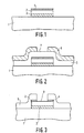
- This passivation layer 5 is deposited by PCVD (plasma activated chemical vapor deposition), as is the case e.g. is described in the above-mentioned reference "Solid State Technology", April l98l, l67 to l7l.
- the passivation layer 5 is then covered in a conventional manner with a photoresist mask 6, which, as shown in FIG. 2, contains an opening 7 through which the passivation layer 5 and the adhesive layer 4 are exposed by a suitable etching method (for example chemical etching or sputter etching) Surface 8 of the metallization layer 2 are removed.
- a suitable etching method for example chemical etching or sputter etching
Landscapes
- Formation Of Insulating Films (AREA)
- Internal Circuitry In Semiconductor Integrated Circuit Devices (AREA)
- Die Bonding (AREA)
- Local Oxidation Of Silicon (AREA)
Applications Claiming Priority (2)
| Application Number | Priority Date | Filing Date | Title |
|---|---|---|---|
| DE19863610709 DE3610709A1 (de) | 1986-03-29 | 1986-03-29 | Verfahren zum herstellen von halbleiter-bauelementen |
| DE3610709 | 1986-03-29 |
Publications (3)
| Publication Number | Publication Date |
|---|---|
| EP0240070A2 true EP0240070A2 (fr) | 1987-10-07 |
| EP0240070A3 EP0240070A3 (en) | 1990-04-25 |
| EP0240070B1 EP0240070B1 (fr) | 1992-10-21 |
Family
ID=6297572
Family Applications (1)
| Application Number | Title | Priority Date | Filing Date |
|---|---|---|---|
| EP87200532A Expired - Lifetime EP0240070B1 (fr) | 1986-03-29 | 1987-03-23 | Procédé pour la fabrication de dispositifs à semi-conducteur |
Country Status (3)
| Country | Link |
|---|---|
| EP (1) | EP0240070B1 (fr) |
| JP (1) | JPS62272557A (fr) |
| DE (2) | DE3610709A1 (fr) |
Families Citing this family (3)
| Publication number | Priority date | Publication date | Assignee | Title |
|---|---|---|---|---|
| JPS644047A (en) * | 1987-06-26 | 1989-01-09 | Toshiba Corp | Semiconductor device |
| JP2558932B2 (ja) * | 1990-07-24 | 1996-11-27 | 松下電器産業株式会社 | 化合物半導体集積回路 |
| JP2007250814A (ja) * | 2006-03-16 | 2007-09-27 | Nippon Telegr & Teleph Corp <Ntt> | 配線構造とその製造方法 |
Family Cites Families (7)
| Publication number | Priority date | Publication date | Assignee | Title |
|---|---|---|---|---|
| US3900944A (en) * | 1973-12-19 | 1975-08-26 | Texas Instruments Inc | Method of contacting and connecting semiconductor devices in integrated circuits |
| US4300149A (en) * | 1979-09-04 | 1981-11-10 | International Business Machines Corporation | Gold-tantalum-titanium/tungsten alloy contact for semiconductor devices and having a gold/tantalum intermetallic barrier region intermediate the gold and alloy elements |
| JPS5848459A (ja) * | 1981-09-16 | 1983-03-22 | Nec Corp | 半導体装置 |
| JPS5860535A (ja) * | 1981-10-06 | 1983-04-11 | Nec Corp | 多層電極の製造方法 |
| JPS59198734A (ja) * | 1983-04-25 | 1984-11-10 | Mitsubishi Electric Corp | 多層配線構造 |
| JPS60103668A (ja) * | 1983-11-10 | 1985-06-07 | Nec Corp | 半導体装置 |
| JPS60119755A (ja) * | 1983-12-01 | 1985-06-27 | Nec Corp | 多層配線半導体集積回路装置 |
-
1986
- 1986-03-29 DE DE19863610709 patent/DE3610709A1/de not_active Withdrawn
-
1987
- 1987-03-23 DE DE8787200532T patent/DE3782264D1/de not_active Expired - Lifetime
- 1987-03-23 EP EP87200532A patent/EP0240070B1/fr not_active Expired - Lifetime
- 1987-03-27 JP JP62071911A patent/JPS62272557A/ja active Pending
Also Published As
| Publication number | Publication date |
|---|---|
| JPS62272557A (ja) | 1987-11-26 |
| EP0240070B1 (fr) | 1992-10-21 |
| DE3782264D1 (de) | 1992-11-26 |
| EP0240070A3 (en) | 1990-04-25 |
| DE3610709A1 (de) | 1987-10-08 |
Similar Documents
| Publication | Publication Date | Title |
|---|---|---|
| DE3853392T2 (de) | Verbindungsstruktur eines Halbleiterbauelementes und Verfahren zu ihrer Herstellung. | |
| DE2402709C3 (de) | Festkörperbauelement mit einem dünnen Film aus Vanadinoxyd | |
| DE1907740A1 (de) | Halbleiteranordnung mit einem wenigstens zwei Halbleiterbereiche entgegengesetzten Leitungstype aufweisenden Halbleiterkoerper | |
| EP0024572A2 (fr) | Structure électroconductive à contact ou à métallisation pour substrats semiconducteurs | |
| DE3414781A1 (de) | Vielschicht-verbindungsstruktur einer halbleitereinrichtung | |
| DE2432719A1 (de) | Verfahren zum erzeugen von feinen strukturen aus aufdampfbaren materialien auf einer unterlage | |
| DE2202520A1 (de) | Metall-Isolieraufbau | |
| DE68922085T2 (de) | Halbleiteranordung und Verfahren zum Herstellen einer Halbleiteranordung. | |
| DE3634168A1 (de) | Halbleitereinrichtung und herstellungsverfahren dafuer | |
| DE69030400T2 (de) | Anordnung der Rückseitenmetallisierung für Halbleiterbauelemente | |
| DE69017520T2 (de) | Metallisierungsprozess. | |
| EP0105189B1 (fr) | Procédé de fabrication d'electrodes métalliques de différentes épaisseurs pour dispositifs à semi-conducteur en particulier pour des dispositifs à semi-conducteur de puissance comme des thyristors | |
| EP0240070B1 (fr) | Procédé pour la fabrication de dispositifs à semi-conducteur | |
| DE2754526A1 (de) | Verfahren zur herstellung einer fotokathode fuer elektroradiographische und elektrofluoroskopische apparate | |
| DE69321265T2 (de) | Verfahren zur Herstellung einer Höckerkontaktstruktur auf einer Halbleiteranordnung | |
| EP0540820A1 (fr) | Méthode de fabrication d'un système de résistance à couche mince structuré et stratifié et circuit avec un système de résistance à couche mince structuré et stratifié fabriqué d'après cette méthode | |
| DE3435750A1 (de) | Verfahren zum erzielen einer konstanten masshaltigkeit von leiterbahnen in integrierten schaltkreisen | |
| EP0967296B1 (fr) | Procédé pour le revêtement d'un substrat | |
| DE19528441A1 (de) | Untermetallisierung für Lotmaterialien | |
| DE1521529C3 (de) | Verfahren zur Herstellung von feinen Strukturen auf einem Substrat | |
| DE1764937C3 (de) | Verfahren zur Herstellung von Isolationsschichten zwischen mehrschichtig übereinander angeordneten metallischen Leitungsverbindungen für eine Halbleiteranordnung | |
| DE4328067C1 (de) | Verfahren zum Aufbringen von metallischen Schichten auf einem nichtmetallischen Substrat unter Einsatz eines Haftvermittlers | |
| DE3534600A1 (de) | Integrierte schaltung mit elektrischen leiterbahnen und verfahren zu ihrer herstellung | |
| DE1942455C3 (de) | Verfahren zum Herstellen mehrschichtiger Leiterbahnen | |
| EP0361572A1 (fr) | Procédé de fabrication des couches conductrices dans les dispositifs semi-conducteurs |
Legal Events
| Date | Code | Title | Description |
|---|---|---|---|
| PUAI | Public reference made under article 153(3) epc to a published international application that has entered the european phase |
Free format text: ORIGINAL CODE: 0009012 |
|
| AK | Designated contracting states |
Kind code of ref document: A2 Designated state(s): DE FR GB IT |
|
| PUAL | Search report despatched |
Free format text: ORIGINAL CODE: 0009013 |
|
| AK | Designated contracting states |
Kind code of ref document: A3 Designated state(s): DE FR GB IT |
|
| 17P | Request for examination filed |
Effective date: 19901023 |
|
| 17Q | First examination report despatched |
Effective date: 19920115 |
|
| GRAA | (expected) grant |
Free format text: ORIGINAL CODE: 0009210 |
|
| AK | Designated contracting states |
Kind code of ref document: B1 Designated state(s): DE FR GB IT |
|
| ITF | It: translation for a ep patent filed | ||
| REF | Corresponds to: |
Ref document number: 3782264 Country of ref document: DE Date of ref document: 19921126 |
|
| GBT | Gb: translation of ep patent filed (gb section 77(6)(a)/1977) |
Effective date: 19930106 |
|
| ET | Fr: translation filed | ||
| PLBE | No opposition filed within time limit |
Free format text: ORIGINAL CODE: 0009261 |
|
| STAA | Information on the status of an ep patent application or granted ep patent |
Free format text: STATUS: NO OPPOSITION FILED WITHIN TIME LIMIT |
|
| 26N | No opposition filed | ||
| ITTA | It: last paid annual fee | ||
| PGFP | Annual fee paid to national office [announced via postgrant information from national office to epo] |
Ref country code: GB Payment date: 19950228 Year of fee payment: 9 |
|
| PGFP | Annual fee paid to national office [announced via postgrant information from national office to epo] |
Ref country code: FR Payment date: 19950329 Year of fee payment: 9 |
|
| ITPR | It: changes in ownership of a european patent |
Owner name: CAMBIO RAGIONE SOCIALE;PHILIPS ELECTRONICS N.V. |
|
| PGFP | Annual fee paid to national office [announced via postgrant information from national office to epo] |
Ref country code: DE Payment date: 19950529 Year of fee payment: 9 |
|
| REG | Reference to a national code |
Ref country code: FR Ref legal event code: CD |
|
| PG25 | Lapsed in a contracting state [announced via postgrant information from national office to epo] |
Ref country code: GB Effective date: 19960323 |
|
| GBPC | Gb: european patent ceased through non-payment of renewal fee |
Effective date: 19960323 |
|
| PG25 | Lapsed in a contracting state [announced via postgrant information from national office to epo] |
Ref country code: FR Effective date: 19961129 |
|
| PG25 | Lapsed in a contracting state [announced via postgrant information from national office to epo] |
Ref country code: DE Effective date: 19961203 |
|
| REG | Reference to a national code |
Ref country code: FR Ref legal event code: ST |
|
| PG25 | Lapsed in a contracting state [announced via postgrant information from national office to epo] |
Ref country code: IT Free format text: LAPSE BECAUSE OF NON-PAYMENT OF DUE FEES;WARNING: LAPSES OF ITALIAN PATENTS WITH EFFECTIVE DATE BEFORE 2007 MAY HAVE OCCURRED AT ANY TIME BEFORE 2007. THE CORRECT EFFECTIVE DATE MAY BE DIFFERENT FROM THE ONE RECORDED. Effective date: 20050323 |