EP0240436A1 - Gleichspannungsvervielfacher, der in eine Halbleiterschicht integriert werden kann - Google Patents
Gleichspannungsvervielfacher, der in eine Halbleiterschicht integriert werden kann Download PDFInfo
- Publication number
- EP0240436A1 EP0240436A1 EP87400743A EP87400743A EP0240436A1 EP 0240436 A1 EP0240436 A1 EP 0240436A1 EP 87400743 A EP87400743 A EP 87400743A EP 87400743 A EP87400743 A EP 87400743A EP 0240436 A1 EP0240436 A1 EP 0240436A1
- Authority
- EP
- European Patent Office
- Prior art keywords
- capacitor
- multiplier
- voltage
- mos
- diode
- Prior art date
- Legal status (The legal status is an assumption and is not a legal conclusion. Google has not performed a legal analysis and makes no representation as to the accuracy of the status listed.)
- Granted
Links
Images

Classifications
-
- H—ELECTRICITY
- H10—SEMICONDUCTOR DEVICES; ELECTRIC SOLID-STATE DEVICES NOT OTHERWISE PROVIDED FOR
- H10D—INORGANIC ELECTRIC SEMICONDUCTOR DEVICES
- H10D84/00—Integrated devices formed in or on semiconductor substrates that comprise only semiconducting layers, e.g. on Si wafers or on GaAs-on-Si wafers
- H10D84/80—Integrated devices formed in or on semiconductor substrates that comprise only semiconducting layers, e.g. on Si wafers or on GaAs-on-Si wafers characterised by the integration of at least one component covered by groups H10D12/00 or H10D30/00, e.g. integration of IGFETs
- H10D84/811—Combinations of field-effect devices and one or more diodes, capacitors or resistors
-
- H—ELECTRICITY
- H02—GENERATION; CONVERSION OR DISTRIBUTION OF ELECTRIC POWER
- H02M—APPARATUS FOR CONVERSION BETWEEN AC AND AC, BETWEEN AC AND DC, OR BETWEEN DC AND DC, AND FOR USE WITH MAINS OR SIMILAR POWER SUPPLY SYSTEMS; CONVERSION OF DC OR AC INPUT POWER INTO SURGE OUTPUT POWER; CONTROL OR REGULATION THEREOF
- H02M3/00—Conversion of DC power input into DC power output
- H02M3/02—Conversion of DC power input into DC power output without intermediate conversion into AC
- H02M3/04—Conversion of DC power input into DC power output without intermediate conversion into AC by static converters
- H02M3/06—Conversion of DC power input into DC power output without intermediate conversion into AC by static converters using resistors or capacitors, e.g. potential divider
- H02M3/07—Conversion of DC power input into DC power output without intermediate conversion into AC by static converters using resistors or capacitors, e.g. potential divider using capacitors charged and discharged alternately by semiconductor devices with control electrode, e.g. charge pumps
-
- H—ELECTRICITY
- H03—ELECTRONIC CIRCUITRY
- H03K—PULSE TECHNIQUE
- H03K17/00—Electronic switching or gating, i.e. not by contact-making and –breaking
- H03K17/06—Modifications for ensuring a fully conducting state
- H03K17/063—Modifications for ensuring a fully conducting state in field-effect transistor switches
-
- H—ELECTRICITY
- H03—ELECTRONIC CIRCUITRY
- H03K—PULSE TECHNIQUE
- H03K17/00—Electronic switching or gating, i.e. not by contact-making and –breaking
- H03K17/51—Electronic switching or gating, i.e. not by contact-making and –breaking characterised by the components used
- H03K17/56—Electronic switching or gating, i.e. not by contact-making and –breaking characterised by the components used by the use, as active elements, of semiconductor devices
- H03K17/687—Electronic switching or gating, i.e. not by contact-making and –breaking characterised by the components used by the use, as active elements, of semiconductor devices the devices being field-effect transistors
-
- H—ELECTRICITY
- H03—ELECTRONIC CIRCUITRY
- H03K—PULSE TECHNIQUE
- H03K17/00—Electronic switching or gating, i.e. not by contact-making and –breaking
- H03K17/30—Modifications for providing a predetermined threshold before switching
- H03K2017/307—Modifications for providing a predetermined threshold before switching circuits simulating a diode, e.g. threshold zero
-
- H—ELECTRICITY
- H03—ELECTRONIC CIRCUITRY
- H03K—PULSE TECHNIQUE
- H03K2217/00—Indexing scheme related to electronic switching or gating, i.e. not by contact-making or -breaking covered by H03K17/00
- H03K2217/0081—Power supply means, e.g. to the switch driver
Definitions
- the present invention relates to a DC voltage multiplier that can be integrated into a semiconductor structure, in particular for controlling a power transistor produced on a semiconductor substrate.
- the power transistor is of the VD MOS type (field effect transistor with vertical structure and diffused channel), to make it conductive, apply a higher voltage to its gate than that existing between its source and its drain.
- the VD MOS and its charge being connected directly to the storage battery, it is therefore necessary to have a DC voltage higher than the battery voltage. Since we do not want to introduce another source of DC voltage in an automobile, we must therefore use a voltage multiplier.
- DC multipliers are known based on the charging and discharging of a capacitor and the control by a clock signal. Such devices include at least two diodes and are made of discrete elements therefore requiring connection wires. Since we want to avoid wiring wires as much as possible, we must integrate this multiplier on the same substrate as the VD MOS. For reasons of simplification of manufacture, it is desired to produce the logic circuit for controlling the VD MOS directly in the substrate which serves as a drain for the VD MOS without particular isolation between the zone constituting the VD MOS and the zone of the logic. We can then take advantage of the diffusion operations which will be used to develop the VD MOS to integrate the diodes mentioned above on the substrate.
- the substrate is of type N
- This solution which seems attractive, cannot however be envisaged. Indeed, it will be impossible to obtain on the grid of the VD MOS a voltage greater than the battery voltage because of the junction formed between the well P of the diode and the N-type substrate which is itself brought to the potential of battery.
- the invention proposes to replace the diode driving the gate of the VD MOS with a resistor formed from a depletion MOS transistor and to modify the duty cycle of the clock signal so that this resistor behaves like the diode of the classic multiplier circuit.
- the voltage multiplier according to the invention has been devised to solve a problem concerning a structure special semiconductor.
- the new electrical diagram thus developed can be used in other applications in the case where a conventional structure is not suitable.
- the subject of the invention is therefore a DC voltage multiplier having a value determined with respect to a reference point and comprising at least one cell of the voltage doubler type by charging and discharging a capacitor and controlling by a signal d clock, the multiplier being intended to supply a control signal to a device having an input capacity of determined value, characterized in that it comprises: electronic means making it possible to set a first electrode of the capacitor to the potential of the reference point as a function of the clock signal, a diode connected to the second electrode of the capacitor and allowing the passage of the charging current under the effect of the DC voltage of determined value, this charging taking place when the first electrode of the capacitor is set to the potential of the reference point, - a resistor connecting the common point between the diode and the capacitor to the device to be controlled, the multiplier also being characterized in that the clock signal has a duty cycle such that the charge time of the capacitor is less than its discharge time.
- the resistance connected to the device to be controlled can advantageously be produced by means of a depletion MOS transistor having its gate connected to one of its two other electrodes.
- the invention also relates to the integration of the voltage multiplier on a semiconductor substrate, in particular when the device to be controlled is a VD MOS produced from an N-type substrate, said depletion MOS transistor being produced from a first P type box, the capacitor being produced from a second P type box.
- said diode will then be constituted by the junction existing between the P-type zone of said first well and the N-type zone of the depletion MOS transistor which is connected to the capacitor.
- FIG. 1 is an electrical diagram representing a VD MOS referenced 1 in series with a load R c .
- This assembly is connected to the terminals of the battery of an automobile and the load R c can for example include the headlights of the vehicle.
- V G the voltage of the drain voltage
- V BAT the voltage of the VD MOS
- FIG. 2 represents the electrical diagram of a DC voltage multiplier of the known art associated with the circuit of FIG. 1.
- FIG. 2 shows the capacitance C ′ existing between the gate and the substrate of the transistor 1.
- the multiplier comprises two diodes D1 and D2 placed in series between the voltage V BAT and the gate of the transistor 1.
- a circuit comprising an inverter 2 in series with a capacitor C is connected to the point P common to the two diodes D1 and D2.
- the input of the inverter is capable of receiving a clock signal S.
- the operation of the device is as follows. If the clock signal S at the input of the inverter is equal to "1", its output is at ground potential and the capacitor C charges at V BAT .
- a diode was made on the left side of the substrate 3, taking advantage of the P and N implantation operations which were used to manufacture the VD MOS.
- the cathode of the diode thus formed is joined by a metallization 6 to the grid of the VD MOS in order to satisfy the electrical diagram of FIG. 2. This manner of proceeding appears satisfactory.
- the capacitor C discharges towards the battery instead of discharging towards the grid of the VD MOS.
- the remedy for this problem would consist in isolating the diode D2 from the rest of the substrate using known solutions (well, buried layer, etc.). However, additional steps are then introduced into the manufacturing process. These additional steps being undesirable, it is necessary to proceed differently.
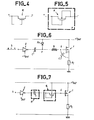
- the invention proposes to replace this diode D2 by a resistor R as shown in FIG. 6 and to modify the duty cycle of the clock signal.
- the duty cycle will preferably be chosen in such a way that the charging time of the capacitor C is low compared to the discharge time of this capacitor towards the gate of the VD MOS.
- the output resistance R ′ of the circuit preceding capacitance C in this case inverter 2 must be sufficiently low compared to resistance R. Correct operation can to be obtained for R ′ about 10 times more small than R and for a duty cycle of the clock signal S of 10 to 20% (that is to say that the duration of the signal S of value "1" is 4 to 9 times shorter than the period of this signal).
- a practical method for carrying out a resistance on a semiconductor substrate is to use a depletion MOS and with channel N.
- This transistor will be carried out starting from a box P which will have to be connected to the most positive potential possible, that is to say ie at the potential + V BAT to minimize the substrate effect.
- one of the two diodes existing between the substrate (that is to say the well P) of the depletion MOS transistor and its source and drain electrodes can be used as diode D1.
- the capacitance C can be obtained from a box P covered with an insulating layer itself covered with an electrode.
- the electrical diagram associated with the semiconductor structure is then that shown in FIG. 7.
- the capacitance C will be obtained from a well P referenced 15 and the N MOS with depletion will be produced from a well P referenced 16.
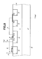
- FIG. 8 represents a semiconductor structure associating a power transistor of the VD MOS type and a DC voltage multiplier.
- This structure was developed from a substrate 20 made of N+ doped silicon and comprising an N-doped epitaxial layer 21. From the epitaxial layer 21, boxes P were produced during the same operation.
- the well 22 will serve as a support for the capacitor C
- the well 23 will serve as a substrate for the N depletion MOS
- the wells 24 and 25 will make it possible to develop the VD MOS.
- Each of the following operations is known per se.
- the N-type zones of the transistors are implanted during the same operation. The development of the transistors poses no problem and will not be described in more detail.
- an insulating layer 26 is deposited followed by a contact 27.
- the insulator can be silicon oxide SiO2 and the contact can be polycrystalline silicon. Connections will be made to connect the gate of the depletion MOS to one of its N-type zones (connection 28), the box 22 at the output of the inverter (connection 29), the contact 27 to one of the ends of the resistor constituted by the N depletion MOS (connection 30), the other end of the resistor to the grid of the VD MOS (connection 31) and the box 23 at potential + V BAT (connection 32).
- the device according to the invention has the advantage of not requiring additional operations.
- the inverter can be easily integrated on the substrate.
- the description has focused on a structure made from an N-type substrate, but adaptation to a P-type substrate is easy.
- the structure developed by the invention results from the solution provided to a series of problems which appeared when it was desired to integrate a DC voltage multiplier on a particular semiconductor substrate.
- the electrical diagram which is the basis of the invention (resistance R, particular duty cycle of the clock signal) could however be used outside the field of semiconductors to solve specific problems.
Landscapes
- Engineering & Computer Science (AREA)
- Power Engineering (AREA)
- Dc-Dc Converters (AREA)
- Semiconductor Integrated Circuits (AREA)
- Metal-Oxide And Bipolar Metal-Oxide Semiconductor Integrated Circuits (AREA)
Applications Claiming Priority (2)
| Application Number | Priority Date | Filing Date | Title |
|---|---|---|---|
| FR8604859 | 1986-04-04 | ||
| FR8604859A FR2596931B1 (fr) | 1986-04-04 | 1986-04-04 | Multiplicateur de tension continue pouvant etre integre a une structure semi-conductrice |
Publications (2)
| Publication Number | Publication Date |
|---|---|
| EP0240436A1 true EP0240436A1 (de) | 1987-10-07 |
| EP0240436B1 EP0240436B1 (de) | 1992-06-17 |
Family
ID=9333915
Family Applications (1)
| Application Number | Title | Priority Date | Filing Date |
|---|---|---|---|
| EP87400743A Expired - Lifetime EP0240436B1 (de) | 1986-04-04 | 1987-04-03 | Gleichspannungsvervielfacher, der in eine Halbleiterschicht integriert werden kann |
Country Status (6)
| Country | Link |
|---|---|
| US (1) | US4796174A (de) |
| EP (1) | EP0240436B1 (de) |
| JP (1) | JP2529165B2 (de) |
| CA (1) | CA1265192A (de) |
| DE (1) | DE3779789T2 (de) |
| FR (1) | FR2596931B1 (de) |
Cited By (4)
| Publication number | Priority date | Publication date | Assignee | Title |
|---|---|---|---|---|
| EP0363020A1 (de) * | 1988-09-20 | 1990-04-11 | Hitachi, Ltd. | Antriebsschaltung |
| EP0398170A3 (de) * | 1989-05-17 | 1991-04-17 | National Semiconductor Corporation | Zeitlich begrenzte Anhebung des Ansteuerstroms für einen DMOS-Transistortreiber mit schnellem Einschalten und niedrigem Ruhestrom |
| EP0582125A1 (de) * | 1992-08-04 | 1994-02-09 | Siemens Aktiengesellschaft | Ansteuerschaltung für einen Leistungs-MOSFET mit sourceseitiger Last |
| EP1081765A3 (de) * | 1999-08-31 | 2001-07-04 | Infineon Technologies AG | Gegen Verpolung geschützte integrierbare Schaltungsanordnung in einem Substrat |
Families Citing this family (19)
| Publication number | Priority date | Publication date | Assignee | Title |
|---|---|---|---|---|
| JP2729062B2 (ja) * | 1987-10-27 | 1998-03-18 | 日本電気株式会社 | 集積回路装置 |
| EP0365706B1 (de) * | 1988-10-27 | 1993-02-03 | Siemens Aktiengesellschaft | Leistungsendstufe mit einer Last |
| US5100821A (en) * | 1989-04-24 | 1992-03-31 | Motorola, Inc. | Semiconductor AC switch |
| US5057707A (en) * | 1989-07-05 | 1991-10-15 | Motorola, Inc. | Charge pump including feedback circuitry for eliminating the requirement of a separate oscillator |
| JP2634685B2 (ja) * | 1990-07-24 | 1997-07-30 | シャープ株式会社 | 半導体装置の電圧降下回路 |
| TW271011B (de) | 1994-04-20 | 1996-02-21 | Nippon Steel Corp | |
| US5666045A (en) * | 1994-12-09 | 1997-09-09 | Psc Inc. | Laser drive and control systems useful for laser diode protection |
| SE504371C2 (sv) * | 1995-02-28 | 1997-01-20 | Ericsson Telefon Ab L M | Anordning och förfarande i telekommunikationssystem för optisk spänningsmultiplicering i integrerad krets |
| US5672992A (en) * | 1995-04-11 | 1997-09-30 | International Rectifier Corporation | Charge pump circuit for high side switch |
| US6166500A (en) * | 1997-07-18 | 2000-12-26 | Siemens Canada Limited | Actively controlled regenerative snubber for unipolar brushless DC motors |
| US6188212B1 (en) | 2000-04-28 | 2001-02-13 | Burr-Brown Corporation | Low dropout voltage regulator circuit including gate offset servo circuit powered by charge pump |
| US6201375B1 (en) | 2000-04-28 | 2001-03-13 | Burr-Brown Corporation | Overvoltage sensing and correction circuitry and method for low dropout voltage regulator |
| US6351159B1 (en) * | 2000-08-08 | 2002-02-26 | Micron Technology, Inc. | Gate coupled voltage support for an output driver circuit |
| JP3688572B2 (ja) * | 2000-09-28 | 2005-08-31 | 株式会社東芝 | 半導体集積回路 |
| EP1221760A3 (de) * | 2001-01-05 | 2002-11-13 | Nokia Corporation | Spannungskombiniererschaltung für elektrische Lasten |
| WO2004066395A2 (en) * | 2003-01-21 | 2004-08-05 | North-West University | Fast switching power insulated gate semiconductor device |
| JP2007252197A (ja) * | 2007-05-02 | 2007-09-27 | Ricoh Co Ltd | 非絶縁降圧型dc−dcコンバータ |
| DE102014112511A1 (de) * | 2014-08-29 | 2016-03-03 | Pintsch Bamag Antriebs- Und Verkehrstechnik Gmbh | Elektronische Steuerungskomponente, Steuermodul mit der elektronischen Steuerungskomponente, Stellgliedeinrichtung mit dem Steuermodul sowie Schranke mit einer solchen Stellgliedeinrichtung |
| US10243451B1 (en) | 2018-03-21 | 2019-03-26 | Dialog Semiconductor (Uk) Limited | System and method for powering a switching converter |
Citations (2)
| Publication number | Priority date | Publication date | Assignee | Title |
|---|---|---|---|---|
| FR2458936A1 (fr) * | 1979-06-12 | 1981-01-02 | Thomson Csf | Dispositif multiplieur de tension pour circuits integres et application a la commande de transistors a effet de champ |
| EP0134731A1 (de) * | 1983-07-08 | 1985-03-20 | Fujitsu Limited | Integrierte Komplementärlogikschaltung |
Family Cites Families (4)
| Publication number | Priority date | Publication date | Assignee | Title |
|---|---|---|---|---|
| US4016476A (en) * | 1972-09-20 | 1977-04-05 | Citizen Watch Co., Ltd. | Booster circuits |
| US4559548A (en) * | 1981-04-07 | 1985-12-17 | Tokyo Shibaura Denki Kabushiki Kaisha | CMOS Charge pump free of parasitic injection |
| JPH061816B2 (ja) * | 1983-09-30 | 1994-01-05 | 日本電気株式会社 | 半導体装置の製造方法 |
| JPH0679262B2 (ja) * | 1984-02-28 | 1994-10-05 | シャープ株式会社 | 参照電圧回路 |
-
1986
- 1986-04-04 FR FR8604859A patent/FR2596931B1/fr not_active Expired - Fee Related
-
1987
- 1987-04-01 US US07/032,560 patent/US4796174A/en not_active Expired - Lifetime
- 1987-04-03 DE DE8787400743T patent/DE3779789T2/de not_active Expired - Fee Related
- 1987-04-03 EP EP87400743A patent/EP0240436B1/de not_active Expired - Lifetime
- 1987-04-03 CA CA000533758A patent/CA1265192A/fr not_active Expired - Lifetime
- 1987-04-04 JP JP62083682A patent/JP2529165B2/ja not_active Expired - Lifetime
Patent Citations (2)
| Publication number | Priority date | Publication date | Assignee | Title |
|---|---|---|---|---|
| FR2458936A1 (fr) * | 1979-06-12 | 1981-01-02 | Thomson Csf | Dispositif multiplieur de tension pour circuits integres et application a la commande de transistors a effet de champ |
| EP0134731A1 (de) * | 1983-07-08 | 1985-03-20 | Fujitsu Limited | Integrierte Komplementärlogikschaltung |
Non-Patent Citations (2)
| Title |
|---|
| NEW ELECTRONICS, vol. 18, no. 13, 25 juin 1985, page 25, Londres, GB; G. PECK AM: "CMOS driver for high treshold MOSFETS" * |
| PATENT ABSTRACTS OF JAPAN, vol. 9, no. 212 (E-339)[1935], 29 août 1985; & JP-A-60 074 665 (NIPPON DENKI K.K.) 26-04-1985 * |
Cited By (5)
| Publication number | Priority date | Publication date | Assignee | Title |
|---|---|---|---|---|
| EP0363020A1 (de) * | 1988-09-20 | 1990-04-11 | Hitachi, Ltd. | Antriebsschaltung |
| EP0398170A3 (de) * | 1989-05-17 | 1991-04-17 | National Semiconductor Corporation | Zeitlich begrenzte Anhebung des Ansteuerstroms für einen DMOS-Transistortreiber mit schnellem Einschalten und niedrigem Ruhestrom |
| EP0582125A1 (de) * | 1992-08-04 | 1994-02-09 | Siemens Aktiengesellschaft | Ansteuerschaltung für einen Leistungs-MOSFET mit sourceseitiger Last |
| US5371418A (en) * | 1992-08-04 | 1994-12-06 | Siemens Aktiengesellschaft | Drive circuit for a power MOSFET with load at the source side |
| EP1081765A3 (de) * | 1999-08-31 | 2001-07-04 | Infineon Technologies AG | Gegen Verpolung geschützte integrierbare Schaltungsanordnung in einem Substrat |
Also Published As
| Publication number | Publication date |
|---|---|
| FR2596931A1 (fr) | 1987-10-09 |
| CA1265192A (fr) | 1990-01-30 |
| DE3779789T2 (de) | 1993-02-18 |
| JP2529165B2 (ja) | 1996-08-28 |
| FR2596931B1 (fr) | 1993-03-26 |
| US4796174A (en) | 1989-01-03 |
| DE3779789D1 (de) | 1992-07-23 |
| EP0240436B1 (de) | 1992-06-17 |
| JPS62239857A (ja) | 1987-10-20 |
Similar Documents
| Publication | Publication Date | Title |
|---|---|---|
| EP0240436B1 (de) | Gleichspannungsvervielfacher, der in eine Halbleiterschicht integriert werden kann | |
| EP2559133B1 (de) | System zur verwaltung einer serienkombination aus stromerzeugungs- oder speicherelementen auf der basis von mehreren spannungsumrichterhalbbrücken | |
| US4814846A (en) | Photoelectric converting device | |
| FR2733094A1 (fr) | Circuit a pompe de charge ameliore pour commutation de cote haut | |
| US4847668A (en) | Device and method of photoelectrically converting light into electrical signal | |
| FR3114441A1 (fr) | Photodiode de type spad | |
| EP0359680B1 (de) | Integrierbare, aktive Diode | |
| EP0614232B1 (de) | Referenzdiode in integriertem Bipolarschaltkreis | |
| EP0638160B1 (de) | Minenräumvorrichtung | |
| EP1608069B1 (de) | Verfahren zur Steuerung eines Analogschalters | |
| EP0755114B1 (de) | Halbleitervorrichtung mit einem Leistungsverstärker und mobilen Telekommunikationsendgerät mit einer solchen Halbleitervorrichtung | |
| FR2666453A1 (fr) | Batterie de photopiles montees en serie. | |
| EP0148086B1 (de) | Hintergrundladungsbeseitigung in einer lichtempfindlichen Festkörperanordnung | |
| EP0012667B1 (de) | Verfahren zum Filtern eines elektrischen Signals durch Ladungsübertragung in einem Halbleiter und Filter mit geschalteten Kondensatoren, das dieses Verfahren verwendet | |
| EP0236200A1 (de) | Halbleiterstruktur, bestehend aus einem oder aus mehreren Hochleistungstransistoren zusammen mit deren Steuerungs- und Schutzlogik | |
| FR2725307A1 (fr) | Composant semiconducteur d'alimentation, de recirculation et de demagnetisation d'une charge selfique | |
| WO1998035312A1 (fr) | Circuit integrateur de charges photogenerees a linearite amelioree | |
| EP3726731A1 (de) | Steuerschaltkreis von transistoren | |
| EP0302789B1 (de) | In vertikaler Integrationstechnologie hergestellter integrierter monolitischer Regulator des Induktionsanregungsstromes eines Wechselstromgenerators mittels einer Wiederdurchflussdiode | |
| EP0220974B1 (de) | Leistungshalbleiterbauteil und damit verbundene Steuerlogik | |
| FR3104862A1 (fr) | Dispositif de commande d’interrupteur | |
| EP0035453A1 (de) | Feldeffekttransistorstruktur mit isoliertem Gate und Verwendung zur Realisierung logischer Gatter | |
| EP1073184A1 (de) | Monolithische Nullspannungssteuerstruktur eines bidirektionalen Schalters mit stabiler Schwellwertspannung | |
| FR2656158A1 (fr) | Photosenseur hybride. | |
| WO1999014803A1 (fr) | Structure microelectronique comportant une partie de basse tension munie d'une protection contre une partie de haute tension et procede d'obtention de cette protection |
Legal Events
| Date | Code | Title | Description |
|---|---|---|---|
| PUAI | Public reference made under article 153(3) epc to a published international application that has entered the european phase |
Free format text: ORIGINAL CODE: 0009012 |
|
| AK | Designated contracting states |
Kind code of ref document: A1 Designated state(s): BE DE ES GB IT NL SE |
|
| 17P | Request for examination filed |
Effective date: 19880328 |
|
| RAP3 | Party data changed (applicant data changed or rights of an application transferred) |
Owner name: THOMSON-CSF |
|
| 17Q | First examination report despatched |
Effective date: 19900319 |
|
| GRAA | (expected) grant |
Free format text: ORIGINAL CODE: 0009210 |
|
| AK | Designated contracting states |
Kind code of ref document: B1 Designated state(s): BE DE ES GB IT NL SE |
|
| PG25 | Lapsed in a contracting state [announced via postgrant information from national office to epo] |
Ref country code: SE Effective date: 19920617 Ref country code: NL Effective date: 19920617 |
|
| ITF | It: translation for a ep patent filed | ||
| REF | Corresponds to: |
Ref document number: 3779789 Country of ref document: DE Date of ref document: 19920723 |
|
| GBT | Gb: translation of ep patent filed (gb section 77(6)(a)/1977) | ||
| PG25 | Lapsed in a contracting state [announced via postgrant information from national office to epo] |
Ref country code: ES Free format text: LAPSE BECAUSE OF FAILURE TO SUBMIT A TRANSLATION OF THE DESCRIPTION OR TO PAY THE FEE WITHIN THE PRESCRIBED TIME-LIMIT Effective date: 19920928 |
|
| NLV1 | Nl: lapsed or annulled due to failure to fulfill the requirements of art. 29p and 29m of the patents act | ||
| PLBE | No opposition filed within time limit |
Free format text: ORIGINAL CODE: 0009261 |
|
| STAA | Information on the status of an ep patent application or granted ep patent |
Free format text: STATUS: NO OPPOSITION FILED WITHIN TIME LIMIT |
|
| PG25 | Lapsed in a contracting state [announced via postgrant information from national office to epo] |
Ref country code: BE Effective date: 19930430 |
|
| 26N | No opposition filed | ||
| BERE | Be: lapsed |
Owner name: THOMSON-CSF Effective date: 19930430 |
|
| PGFP | Annual fee paid to national office [announced via postgrant information from national office to epo] |
Ref country code: DE Payment date: 20010326 Year of fee payment: 15 |
|
| PGFP | Annual fee paid to national office [announced via postgrant information from national office to epo] |
Ref country code: GB Payment date: 20010328 Year of fee payment: 15 |
|
| REG | Reference to a national code |
Ref country code: GB Ref legal event code: IF02 |
|
| PG25 | Lapsed in a contracting state [announced via postgrant information from national office to epo] |
Ref country code: GB Free format text: LAPSE BECAUSE OF NON-PAYMENT OF DUE FEES Effective date: 20020403 |
|
| PG25 | Lapsed in a contracting state [announced via postgrant information from national office to epo] |
Ref country code: DE Free format text: LAPSE BECAUSE OF NON-PAYMENT OF DUE FEES Effective date: 20021101 |
|
| GBPC | Gb: european patent ceased through non-payment of renewal fee |
Effective date: 20020403 |
|
| PG25 | Lapsed in a contracting state [announced via postgrant information from national office to epo] |
Ref country code: IT Free format text: LAPSE BECAUSE OF NON-PAYMENT OF DUE FEES;WARNING: LAPSES OF ITALIAN PATENTS WITH EFFECTIVE DATE BEFORE 2007 MAY HAVE OCCURRED AT ANY TIME BEFORE 2007. THE CORRECT EFFECTIVE DATE MAY BE DIFFERENT FROM THE ONE RECORDED. Effective date: 20050403 |