EP0363020A1 - Antriebsschaltung - Google Patents
Antriebsschaltung Download PDFInfo
- Publication number
- EP0363020A1 EP0363020A1 EP89309125A EP89309125A EP0363020A1 EP 0363020 A1 EP0363020 A1 EP 0363020A1 EP 89309125 A EP89309125 A EP 89309125A EP 89309125 A EP89309125 A EP 89309125A EP 0363020 A1 EP0363020 A1 EP 0363020A1
- Authority
- EP
- European Patent Office
- Prior art keywords
- switching element
- switching
- power source
- storage device
- charge storage
- Prior art date
- Legal status (The legal status is an assumption and is not a legal conclusion. Google has not performed a legal analysis and makes no representation as to the accuracy of the status listed.)
- Granted
Links
- 239000004065 semiconductor Substances 0.000 claims description 29
- 239000000758 substrate Substances 0.000 claims description 6
- 230000001681 protective effect Effects 0.000 claims description 4
- 230000002457 bidirectional effect Effects 0.000 claims description 2
- 238000000034 method Methods 0.000 claims description 2
- 239000003990 capacitor Substances 0.000 abstract description 80
- 238000010304 firing Methods 0.000 description 4
- 238000010791 quenching Methods 0.000 description 4
- 238000010276 construction Methods 0.000 description 2
- 238000007599 discharging Methods 0.000 description 1
- 230000003071 parasitic effect Effects 0.000 description 1
- 230000000171 quenching effect Effects 0.000 description 1
- 238000007493 shaping process Methods 0.000 description 1
Images



Classifications
-
- H—ELECTRICITY
- H02—GENERATION; CONVERSION OR DISTRIBUTION OF ELECTRIC POWER
- H02M—APPARATUS FOR CONVERSION BETWEEN AC AND AC, BETWEEN AC AND DC, OR BETWEEN DC AND DC, AND FOR USE WITH MAINS OR SIMILAR POWER SUPPLY SYSTEMS; CONVERSION OF DC OR AC INPUT POWER INTO SURGE OUTPUT POWER; CONTROL OR REGULATION THEREOF
- H02M7/00—Conversion of AC power input into DC power output; Conversion of DC power input into AC power output
- H02M7/42—Conversion of DC power input into AC power output without possibility of reversal
- H02M7/44—Conversion of DC power input into AC power output without possibility of reversal by static converters
- H02M7/48—Conversion of DC power input into AC power output without possibility of reversal by static converters using discharge tubes with control electrode or semiconductor devices with control electrode
- H02M7/53—Conversion of DC power input into AC power output without possibility of reversal by static converters using discharge tubes with control electrode or semiconductor devices with control electrode using devices of a triode or transistor type requiring continuous application of a control signal
- H02M7/537—Conversion of DC power input into AC power output without possibility of reversal by static converters using discharge tubes with control electrode or semiconductor devices with control electrode using devices of a triode or transistor type requiring continuous application of a control signal using semiconductor devices only, e.g. single switched pulse inverters
- H02M7/538—Conversion of DC power input into AC power output without possibility of reversal by static converters using discharge tubes with control electrode or semiconductor devices with control electrode using devices of a triode or transistor type requiring continuous application of a control signal using semiconductor devices only, e.g. single switched pulse inverters in a push-pull configuration
-
- H—ELECTRICITY
- H02—GENERATION; CONVERSION OR DISTRIBUTION OF ELECTRIC POWER
- H02M—APPARATUS FOR CONVERSION BETWEEN AC AND AC, BETWEEN AC AND DC, OR BETWEEN DC AND DC, AND FOR USE WITH MAINS OR SIMILAR POWER SUPPLY SYSTEMS; CONVERSION OF DC OR AC INPUT POWER INTO SURGE OUTPUT POWER; CONTROL OR REGULATION THEREOF
- H02M3/00—Conversion of DC power input into DC power output
- H02M3/02—Conversion of DC power input into DC power output without intermediate conversion into AC
- H02M3/04—Conversion of DC power input into DC power output without intermediate conversion into AC by static converters
- H02M3/06—Conversion of DC power input into DC power output without intermediate conversion into AC by static converters using resistors or capacitors, e.g. potential divider
- H02M3/07—Conversion of DC power input into DC power output without intermediate conversion into AC by static converters using resistors or capacitors, e.g. potential divider using capacitors charged and discharged alternately by semiconductor devices with control electrode, e.g. charge pumps
-
- H—ELECTRICITY
- H03—ELECTRONIC CIRCUITRY
- H03K—PULSE TECHNIQUE
- H03K17/00—Electronic switching or gating, i.e. not by contact-making and –breaking
- H03K17/06—Modifications for ensuring a fully conducting state
- H03K17/063—Modifications for ensuring a fully conducting state in field-effect transistor switches
-
- H—ELECTRICITY
- H03—ELECTRONIC CIRCUITRY
- H03K—PULSE TECHNIQUE
- H03K17/00—Electronic switching or gating, i.e. not by contact-making and –breaking
- H03K17/08—Modifications for protecting switching circuit against overcurrent or overvoltage
- H03K17/082—Modifications for protecting switching circuit against overcurrent or overvoltage by feedback from the output to the control circuit
- H03K17/0822—Modifications for protecting switching circuit against overcurrent or overvoltage by feedback from the output to the control circuit in field-effect transistor switches
Definitions
- the present invention relates to a driving circuit which may be formed as a semiconductor circuit for use in a power IC.
- a bridge inverter for driving a load such as a motor by connecting in series two identical voltage- switching elements.
- Those switching elements are connected across a main d.c. voltage source, with the switching element connected to the high potential side of that source being referred to as an upper arm switching element and the switching element connected to the low potential side of the voltage source being referred to as a lower arm switching element.
- a drive voltage may be generated at their point of interconnection, which drive voltage may be applied to the load.
- each phase requires a corresponding pair of upper and lower arm switching elements, and all the lower arms switching elements may be driven from a single power source.
- a separate D.C. insulated power source is required to drive each upper arm switching element, which makes the resulting circuit complex and expensive.
- the voltage drop across the capacitor is affected when the lower arm switching element is turned on, and the prior art does not provide any method of compensating for firing the lower arm switching element.
- the charging of the capacitor depends on the potential of the interconnection of the two switching elements, which is not satisfactory.
- a further disadvantage of the known system is that the driving power to the motor is affected by the power needed to charged the capacitor(s). Again, this is undesirable.
- the present invention seeks to provide a driving circuit in which the switching of the upper arm switching element may be simiplified, particularly but not exclusively in a polyphase circuit.
- a charge storage device e.g. a capacitor
- suitable charging means may be provided connected to a secondary D.C. power source.
- the present invention originates in a desire to improve a driving circuit having a pair of switching elements connected in parallel across a primary D.C. power source.
- the present invention is also applicable to driving circuits having only one switching element.
- a corresponding plurality of upper arm switching elements may be provided, but all may be connected in common to the charge storage device.
- a first switching means may be provided between the charge storage device and the control terminal of that switching element.
- a second switching means may be provided between the control terminal of that switching element and the low potential side of the main D.C. voltage source.
- a third switching means and a suitable resistance may be provided between the control terminal and the upper arm switching element and the low potential side of the main D.C. power source.
- a protective bi-directional voltage diode may also be provided in parallel to that for switching means.
- the charge storage device (capacitor) is charged by a suitable charging circuit which is powered from a secondary power source, which may be the driving power source for the lower arm switching element. Therefore, the capacitor can be charged independently of the operation of the lower arm switching element (and indeed independent of the operation of the upper arm switching element) so that the capacitor may supply a stable drive to the upper arm switching element.
- the upper arm switching element is turned on by control of the first switch between the high potential side of the capacitor and the control terminal of the upper arm switching element, and to turn off the upper arm switching element the first switch disconnects the capacitor from the control terminal, and the second switch connects the control terminal to the low voltage side of the main D.C. voltage source. This turns off the upper arm switching element, and the on- period of the second switching means may be shorter than the off-period, since all that is needed is a pulse to trigger the upper arm switching element.
- a suitable circuit may be provided to protect the control terminal from the forward-biased voltage applied thereto.
- operation of the third switching means in series with the second, connects the control terminal to the low potential side of the main D.C. voltage source through a resistance, so that the upper arm switching element is reverse biased. Equally, when the voltage of connection point is at a similar level to the low potential side of the main D.C.
- a voltage detector connected between the high potential side of the main D.C voltage source and the interconnection point causes turning on of the fourth switching means connected between the control terminal and the interconnection point, thereby short circuiting the control terminal to prevent erronous firing of the upper arm switching element.
- Two constant voltage diodes may be mounted in opposite directions between the control terminal and the interconnection point to prevent the application of an excessive voltage to the switching element.
- a protection circuit may be provided for detecting the voltage across the capacitor and controlling the operation of at least the lower arm switching element independently of that voltage.
- Fig. 1 shows a semiconductor driving circuit according to the invention with a first d.c power source (primary voltage source) 1 with a voltage of E.
- the voltage source 1 an upper arm switching element 7 and a lower arm switching element 8 from a closed circuit with the latter two elements connected in series with the primary voltage source 1.
- One side of a capacitor 2 is connected to the high potential side of the primary voltage source 1 to form a first charge storage means, and the other side of the capacitor 2 is connected to a capacitor charging circuit 3 and an upper arm driving circuit 5.
- the capacitor charging circuit 3 is connected to both sides of the primary voltage source 1 and the high potential side of a second D.C. power source (secondary voltage source) 4 whose voltage is Vcc.
- the upper arm driving circuit is connected to both sides of the primary voltage source 1, a control terminal arm switching element 7, and a mid-point potential contact 12.
- the lower arm driving circuit 6 is connected to both ends of the secondary voltage source 4 and a control terminal of the lower arm switching elememt 8.
- the lower potential side of the primary voltage source 1 is connected to that of the secondary voltage source 4, which is grounded in a manner that allows both sides to stay at the same potential.
- a voltage detecting circuit 10 is connected to both ends of the capacitor 2 and supplied a detecting signal to a control circuit 11.
- the control circuit 11 is connected to a voltage detecting circuit 10 and receives a status signal from that voltage detecting circuit 10. In response to the status signal, the control circuit 11 supplies a control signal to the capacitor charging circuit 3, the upper arm driving circuit 5, and the lower arm driving circuit 6.
- a load e.g. a motor
- the other end of the load 9 is connected to a contact between two magnetic field capacitors 9-1 and 9-2, which are respectively connected in series to the high potential and low potential sides of the voltage source 1.
- the low potential side of the lower arm switching element 8 is connected to a protective circuit (surge current detector) 40.
- surge current detector 40 transmits a surge current detecting signal to the control circuit 11.
- the control circuit 11 immediately supplies signals to the upper arm driving circuit 5 and the lower arm driving circuit 6 to stop the drive of the switching elements 7 and 8. Furthermore it supplies a charging signal to the capacitor charging circuit 3 so that the capacitor 2 is continuously charged.
- the surge current detector 40 is provided only for the lower arm switching element 8 side, but a further detector may also be provided at the upper arm switching element 7.
- the capacitor charging circuit 3 switches on and off a switch contained inside the circuit in response to a signal from the control circuit 11 such that the capacitor 2 is charged by the secondary voltage source 4.
- the voltage detecting circuit 10 charges to allow the control circuit 11 to output a signal.
- the control circuit 11 receives a signal from the voltage detecting circuit 10 and outputs a driving signal to the upper arm driving circuit 6.
- a voltage is applied to the mid-point voltage contact 12, i.e. to the load 9 to alternately switch between two circuit states, namely the on-state of the upper arm switching element 7 and the on-state of the lower arm switching element 8.
- the charging capacitors 9-1 and 9-2 stabilize the voltage to be applied to the load 9.
- the control circuit 11 controls the frequency and on-period of the driving signal.
- the switching element driving power source need use only the secondary voltage source 4 only, since the capacitor 2 and the capicitor charging circuit 3 drive the upper arm switching element 7.
- the capacitor charging circuit 3 can operate independently of the operating states of the uppper arm switching element 7 and the lower arm switching element 8, so it does not influence the load 9.
- the voltage detecting circuit 10 and a means. for outputting the detecting signal to the control circuit 11 enable the upper arm side switching element to start driving when the ccapacitor voltage rises to the required voltage.
- Fig. 2 shows a second embodiment wherein the present invention is used to form a three-phase full-bridge inverter for driving a three phase motor 9.
- the second embodiment difffers from the first embodiment in that driving circuits are required for main switches to operate three upper arm switching elements 7-1, 7-2, and 7-3 (each corresponding to the upper arm switching element 7 of Fig. 1) and three lower arm switching elements 8-1, 8-2, and 8-3, (each corresponding to the lower arm switching element 8 of Fig. 1).
- the feature of this embodiment is that the capacitor 2 is a common power source for the three upper arm side switching elements 7-1, 7-2, and 7-3. This arrangement makes it possible greatly to reduce the number of parts, because it is possible to eliminate separate driving power sources to drive the upper arm side switching elements 7-1, 7-2m and 7-3.
- Fig. 3 shows a third embodiment of the present inventioon wherein the present invention is applied to a high-side switch.
- a primary voltage source 1, a capacitor 2, a secondary voltage source 4, a capacitor charging circuit 3, and a voltage detecting circuit 10 respectively have the same arrangment as in Fig. 1.
- Fig. 3 shows the driving circuit 5-4 for a switching element 7-4.
- a load 9, the voltage source, 1 and the switching element 7-4 compose a closed circuit.
- the switching element 7-4 is a high-side switch located at the high potential side of the load 9.
- the control circuit 11 is driven by the secondary voltage source 4 and is connected to the voltage detecting circuit 10, the capacitor charging circuit 3, and the driving circuit 5-4.
- the capacitor charging circuit 3 charges the capacitor 2 using the secondary voltage source 4.
- the voltage detecting circuit 10 supplies a signal to the control circuit 11.
- the control circuit 11 supplies a signal to drive the switching element 7-4 to the driving circuit 5-4.
- control circuit 11, the load 9, and the ground potential employ a commmon voltage source (the secondary voltage source 4) as the power source for the control circuit 11 and for charging the capacitor 2.
- the embodiment makes it possible to employ a common power source as the control power source and switching element driving power source, so as to reduce the number of parts.
- the third embodiment differs from the first embodiment in that there is no lower arm switching element, but only a single switching element 7-4.
- Fig. 4 shows a fourth embodiment of the invention.
- all the components of the circuit bonded by dotted line 13 are formed on a single semiconductor chip. That chip is connected to a voltage source 1 whose voltage is E and a voltage source 3 whose voltage is Vcc.
- the main semiconductor driving may include the corresponding components indicated in Fig. 1 or in Fig. 3 (depending on whether there are two switching elements or only one), and thus may have a charging circuit for a capacitor 2, a switching element, a driving circuit for thw switching element, etc. as in Fig. 1 or Fig. 3.
- the semiconductor circuit 13 is connected to the primary voltage source 1, the secondary voltage source 4 and the capacitor 2 through terminals.
- the voltage detecting circuit 10 and the main semiconductor driving circuit 14 respectively supply the external terminals 15-1 and 15-3.
- the semiconductor circuit 13 also provides an external terminal to be connected to a load.
- the main semiconductor driving circuit 14 includes a charging circuit for the capacitor 2, which uses charges from the secondary voltage source 4 for charging the capacitor 2. When the capacitor 2 is charged to a higher voltage than the required value, the circuit outputs a signal to the terminal 15-1.
- the control circuit (not shown in Fig, 4) of the semiconductor circuit 13 connected to the external source supplies a control signal to the main semiconductor driving circuit 14 through the terminal 15-2 in response to the signal from the terminal 15-1.
- the main semiconductor driving circuit 14 switches on and off the switching element(s) to allow a voltage to be applied to the load through the output terminal.
- the circuit for detecting the level of the capacitor 2 voltage and the terminal 15-1 for transmitting that level to the exterior make it possible to prevent the main semiconductor driving circuit 14 from operating abnormally, such as increasing the on-resistance of a main resistor resulting from lack of voltage of the capacitor 2 for driving the semiconductor main driving circuit 14.
- Fig. 5 shows a fifth embodiment of the present invention.
- the arrangement and circuit operation of this embodiment are basically similar to that of the embodiment shown in Fig. 4 and detailed description of the components which are common to the embodiments of Figs. 4 and 5 will be omitted.
- a logic circuit 16 is connected to the terminal 15-1 interposed between the voltage detecting circuit 10 and the exterior and to the terminal 15-2 for transmitting a control signal to the one-chip semiconductor circuit 13.
- the logic circuit 16 is also connected to the semiconductor main driving circuit 14.
- This circuit arrangmenet allows the logic circuit 16 to screen the control signal sent from the terminal 15-2 to the semicoonductor main driving circuit 14 until the voltage of capacitor 2 becomes equal to or more than a given value.
- the circuit By adding the logic circuit 16, it is possible for the circuit to self-diagnose the lack of a driving voltage for the switching element from the capacitor 2 for the main semiconductor driving circuit 14 or to protect the switching element.
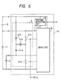
- Fig. 6 shows a detailed circuit arrangement for the capacitor changing circuit 3 for use in embodiments according to the invention.
- the one-chip semiconductor circuit 13 is connected to the primary voltage source 1, the secondary voltage source 4 and the capacitor 2. Inside the semiconductor circuit 13 are a main semiconductor driving circuit 14 as shown in Fig. 4 but in Fig. 6, circuit 14 excludes the capacitor charging circuit, and a separate capacitor charging circuit 3 is shown. These circuits have the same connections as described in the previous embodiments.
- the capacitor charging circuit 3 comprises switches 3-1, 3-2, diodes 3-3, 3-4, and a capacitor 3-5.
- a closed circuit is formed such as to allow the high potential side terminal of the primary voltage source 1 to be connected in series to switches 3-1 and 3-2 and the switch 3-2 to be connected to the low potential side of the primary voltage source 1.
- diodes 3-4 and 3-3 are connected in series between the high potential side of the secondary voltage source 4 and that of the primary voltage source 1 to allow the capacitor 2 to direct its high potential to a cathode electrode.
- One side of tha capacitor 3-5 is connected to a contact between the diodes 3-4 and 3-3 and the other end is connected to a contact between switches 3-1 and 3-2.
- the switches 3-1 and 3-2 are repeatedly and alternately turned on and off.
- the capacitor charging circuit 3 moves charges from the secondary voltage source 4 to the capicitor 2.
- the switch 3-2 When the switch 3-2 is switched on, the secondary voltage source 4, the diode 3-4, the capacitor 3-5, and the switch 3-2 form a closed circuit. Current flowing from the voltage source 4 to the capacitor 3-5 enables the capacitor 3-5 to be charged.
- the capacitor 2 can be discharged by repeatedly alternating the two circuit states stated above.
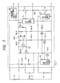
- Fig. 7 shows an embodiment wherein a level shift circuit is added to the embodiment shown in Fig. 6.
- a constant voltage diode 26-2 Between the control terminal 27 of the switch 3-1 and the high potential side of the voltage source 1 are connected a constant voltage diode 26-2, a resistor 24-4, and a MOSFET 25-3.
- a resistor 24-3 and MOSFET 25-2 are connected in series between the resistor 24-4 and the MOSFET 25-3.
- a resistor 24-2 and a constant voltage diode 26-1 are connected in parallel between a control terminal 28 of the MOSFET 25-3 and the high potential side of the voltage source 1.
- a resistor 24-1 and a MOSFET 25-1 are connected in series between the control terminal 28 and the low potential side of the voltage source.
- the switch 3-1 is a p-channel type MOSFET, in order to turn on this switch 3-1 it is necessary to switch on the MOSFET 25-2 and to apply a voltage that is separate from the primary voltage source 1 through the resistors 24-3 and 24-4 between the high potential side of the primary voltage source 1 and the terminal 27.
- To quench the switch 3-1 it is necessary to switch off the MOSFET 25-2 and switch on the MOSFET 25-1, fire the MOSFET 25-3 with a voltage drop caused by resistor 24-2, short circuit the high potential side of the primary voltage source 1 with the terminal 27, and then to rapidly quench the switch 3-1.
- Constant voltage diodes 26-2 and 26-1 are connected reprectively between the terminal 27 and the high potential side of the primary voltage source 1 and between the terminal 28 and the primary voltage source 1.
- the circuit is very simple since it comprises two diodes, two switches and one capacitor; the capacitor 3-5 provided outside the semiconductor circuit 13 as shown in Fig. 7 enables the semiconductor circuit to be formed on a single chip, so that the MOSFET, the resistors, the constant voltage diode, and the diode are integrated.
- the diode and MOSFET have some elements requiring voltage-proofing for the primary voltage source 1, the current flowing is far smaller than that flowing through the switching element 7 so the component areas may be small.
- this embodiment is appropriate for a circuit incorporating the upper arm driving circuit 5, the lower arm driving circuit 6, and the switching elements 7, 8 on one semiconductor substrate in particular a high-voltage-proof IC.
- Fig. 8 shows a detail of the driving circuit 5 of the switching element 7 at the high potential side of the voltage source included in the invention.
- Fig. 8 shows the primary voltage source 1, a capacitor 2 an upper arm switching element 7 and a lower arm switching element 8. These units employ an n-channel type MOSFETs. These units do not need to be described since they have the same construction as those shown in Fig. 1. Next, reference wil be made to the construction an doperation of the driving circuit of th eipper arm side switching element 7.
- a switch 17-1 is connected between the high potential side of the capacitor 2 and a control terminal 22 of the upper arm switching element 7.
- Connected in series between the control terminal 22 and the low potential side of the voltage source 1 are a switch 17-2, a resistor 21-1, and a switch 17-3.
- a bideirectional constant voltage means 19-1 and a switch 17-4 are connected between the control terminal 22 and the mid-point potential contact 12.
- the switch 17-4 employs an n-channel type MOSFET.
- a bidirectional constant voltage means 19-2 is connected between the constant terminal 23 of the switch 7-4 and the mid-point potential contact 12.
- Connected in series between the high potential side of the primary voltage source 1 and the control terminal 23 are a diode 18, a constant voltage means 19-3, and a resistor 21-2 of large resistance.
- the switches 17-1 and 17-5 must be turned onto fire the upper arm switching element 7, resulting in a current flowing through a closed circuit formed by the high potential side of the capacitor, the switch 17-1, the constant voltage means 19-1, the reverse-parallel diode of the upper arm switching element 7, and the low potential side of the capacitor 2 in that order.
- the current forward-biases the control terminal 22 and the mid-point potential contact 12 so that the upper arm switching element 7 is fired.
- the constant voltage means 19-3 remains in a conducting state, the current flowing through the resistor 21-2 serves to forward-bias a voltage between the control terminal 23 and the mid-point potential contact 12, switch 17-4 is turned on, and the control terminal 22 is short-circuited with the mid-point potential contact 12.
- the switching means 20 short circuit the control terminal 23 and the mid-point potential contact 12, and then turn off the switch 17-4.
- the mid-point potential contact 12 When the upper arm switching element 7 is quenched it cannot be fired in error if the mid-point potential contact 12 is subject to a dv/dt variation resulting from the change in state of the main circuit. When current flows as a result of the upper arm side reverse-parallel diode remaining on, the mid-point potential contact 12 is at a similar voltage level to the primary voltage source 1. Turning on the switch 17-3 therefore causes a microcurrent to flow through the constant voltage means 19-1 and the resistor 21-2 so as not to apply a forward-biased voltage to the upper arm switching element 7.
- the mid-point potential contact 12 stays at a similar potential to the low potential side of the voltage source 1. Since the constant voltage means 19-3 is in a conducting state as stated above, the control terminal 22 is short-circuited with the mid-point potential contact 12 by forward-biasing the switch 17-4 so as not to apply a forward biased voltage on the upper arm switching element 7. Hence, the upper arm side switching element 7 is not fired erroneously when the mid-point potential contact 12 is subject to a dv-dt variation.
- the diode 18 is used to prevent reverse current.
- the important feature is the firing the upper arm switching element 7 with the charges stored in the capacitor 2, turning on the switching 17-2, applying a reverse-biased voltage on the upper arm switching element 7, and rapidly quenching it. Moreover, it has an additional feature of stopping erroneous firing of the upper arm switching element 7 when the mid-point potential contact 12 is subject to a dv/dt variation.
- the circuit arrangement needs a high voltage-proof element as a switch, it can be integrated as shown in the embodiment in Fig. 7, and is appropriate for a high voltage-proof IC formed on a single substrate.
- IGBT Insulated Gate Bipolar Transistor
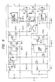
- Fig. 9 shows an arrangement wherein such a level shift circuit is added to the embodiment shown in Fig. 8.
- the level shift circuit comprises switches 31-1 and 31-2, resistors 33-1 to 33-4, constant voltage diodes 34-1 and 34-2, and a MOSFET 35.
- the aspects of the circuit that differ from the level shift circuit shown in Fig. 7 are that the potential at the high potential side conforms to that at the high potential side of the capacitor in Fig. 9, while also confirming to that at the high potential side of the primary voltage source 1 in Fig. 7, and that inverter circuits 29-1 and 29-2 are newly added. These inverter circuits 29-1 and 29-2 are used for wave shaping.
- the switches 31-1, 31-2 and 17-2, 17-3 are connected to a logic circuit 32. These switches are driven by a signal, which is the driving signal of the upper arm side switching element 7 of logic circuit 32. The signal is received at the terminal 30-2.
- constant voltage diodes are replaced with the constant voltage means 19-1 to 19-3, and the switching circuit 20 employs a constant current mirror circuit composed of bipolar transistors.
- the present invention makes it possible to employ a capacitance on the high potential side of a bridge inverted primary D.C. voltage source as a driving power source common to each phase of an upper arm side switching element, and thereby to reduce the number of components in the circuit.
Landscapes
- Engineering & Computer Science (AREA)
- Power Engineering (AREA)
- Power Conversion In General (AREA)
- Inverter Devices (AREA)
- Semiconductor Integrated Circuits (AREA)
- Dc-Dc Converters (AREA)
- Electronic Switches (AREA)
Applications Claiming Priority (2)
| Application Number | Priority Date | Filing Date | Title |
|---|---|---|---|
| JP63233431A JP2791049B2 (ja) | 1988-09-20 | 1988-09-20 | 半導体駆動回路 |
| JP233431/88 | 1988-09-20 |
Publications (2)
| Publication Number | Publication Date |
|---|---|
| EP0363020A1 true EP0363020A1 (de) | 1990-04-11 |
| EP0363020B1 EP0363020B1 (de) | 1993-12-22 |
Family
ID=16954934
Family Applications (1)
| Application Number | Title | Priority Date | Filing Date |
|---|---|---|---|
| EP89309125A Expired - Lifetime EP0363020B1 (de) | 1988-09-20 | 1989-09-08 | Antriebsschaltung |
Country Status (4)
| Country | Link |
|---|---|
| EP (1) | EP0363020B1 (de) |
| JP (1) | JP2791049B2 (de) |
| KR (1) | KR0133530B1 (de) |
| DE (1) | DE68911638T2 (de) |
Cited By (3)
| Publication number | Priority date | Publication date | Assignee | Title |
|---|---|---|---|---|
| EP0782235A1 (de) * | 1995-12-29 | 1997-07-02 | STMicroelectronics S.r.l. | Verfahren zum Schutz von Leistungstransistoren und übereinstimmende Schaltung |
| EP0689292A3 (de) * | 1994-06-17 | 1997-10-22 | Harris Corp | Ansteuerschaltung für Brückenschaltungen und entsprechendes Verfahren |
| WO2000001069A1 (de) * | 1998-06-26 | 2000-01-06 | Siemens Aktiengesellschaft | Elektronisches abzweigschaltgerät |
Families Citing this family (2)
| Publication number | Priority date | Publication date | Assignee | Title |
|---|---|---|---|---|
| JP2908948B2 (ja) * | 1992-12-10 | 1999-06-23 | 三菱電機株式会社 | パワーデバイスの制御回路及び半導体集積回路装置 |
| JP5194421B2 (ja) * | 2006-10-12 | 2013-05-08 | オムロン株式会社 | スイッチング電源装置 |
Citations (5)
| Publication number | Priority date | Publication date | Assignee | Title |
|---|---|---|---|---|
| US4636930A (en) * | 1985-10-01 | 1987-01-13 | Maxim Integrated Products, Inc. | Integrated dual charge pump power supply and RS-232 transmitter/receiver |
| EP0229482A2 (de) * | 1986-01-13 | 1987-07-22 | General Motors Corporation | Feldeffekttransistor verwendender Schaltkreis und Spannungsregler |
| US4691271A (en) * | 1985-10-28 | 1987-09-01 | Northern Telecom Limited | Voltage multiplier and voltage multipliers in an amplifier with double rail output |
| EP0240436A1 (de) * | 1986-04-04 | 1987-10-07 | Thomson-Csf | Gleichspannungsvervielfacher, der in eine Halbleiterschicht integriert werden kann |
| EP0297545A2 (de) * | 1987-07-01 | 1989-01-04 | Hitachi, Ltd. | Leistungsversorgungsschaltung |
Family Cites Families (2)
| Publication number | Priority date | Publication date | Assignee | Title |
|---|---|---|---|---|
| JPS5389356A (en) * | 1977-01-17 | 1978-08-05 | Hitachi Ltd | Control unit for gate off thyristor |
| JPS59226674A (ja) * | 1983-06-07 | 1984-12-19 | Fuji Electric Co Ltd | 電力変換装置 |
-
1988
- 1988-09-20 JP JP63233431A patent/JP2791049B2/ja not_active Expired - Lifetime
-
1989
- 1989-09-08 EP EP89309125A patent/EP0363020B1/de not_active Expired - Lifetime
- 1989-09-08 DE DE89309125T patent/DE68911638T2/de not_active Expired - Lifetime
- 1989-09-20 KR KR1019890013532A patent/KR0133530B1/ko not_active Expired - Fee Related
Patent Citations (5)
| Publication number | Priority date | Publication date | Assignee | Title |
|---|---|---|---|---|
| US4636930A (en) * | 1985-10-01 | 1987-01-13 | Maxim Integrated Products, Inc. | Integrated dual charge pump power supply and RS-232 transmitter/receiver |
| US4691271A (en) * | 1985-10-28 | 1987-09-01 | Northern Telecom Limited | Voltage multiplier and voltage multipliers in an amplifier with double rail output |
| EP0229482A2 (de) * | 1986-01-13 | 1987-07-22 | General Motors Corporation | Feldeffekttransistor verwendender Schaltkreis und Spannungsregler |
| EP0240436A1 (de) * | 1986-04-04 | 1987-10-07 | Thomson-Csf | Gleichspannungsvervielfacher, der in eine Halbleiterschicht integriert werden kann |
| EP0297545A2 (de) * | 1987-07-01 | 1989-01-04 | Hitachi, Ltd. | Leistungsversorgungsschaltung |
Non-Patent Citations (1)
| Title |
|---|
| PATENT ABSTRACTS OF JAPAN * |
Cited By (4)
| Publication number | Priority date | Publication date | Assignee | Title |
|---|---|---|---|---|
| EP0689292A3 (de) * | 1994-06-17 | 1997-10-22 | Harris Corp | Ansteuerschaltung für Brückenschaltungen und entsprechendes Verfahren |
| EP0782235A1 (de) * | 1995-12-29 | 1997-07-02 | STMicroelectronics S.r.l. | Verfahren zum Schutz von Leistungstransistoren und übereinstimmende Schaltung |
| US5831466A (en) * | 1995-12-29 | 1998-11-03 | Sgs Thomson Microelectronics S.R.L. | Protection method for power transistors, and corresponding circuit |
| WO2000001069A1 (de) * | 1998-06-26 | 2000-01-06 | Siemens Aktiengesellschaft | Elektronisches abzweigschaltgerät |
Also Published As
| Publication number | Publication date |
|---|---|
| JPH0284055A (ja) | 1990-03-26 |
| DE68911638D1 (de) | 1994-02-03 |
| DE68911638T2 (de) | 1994-04-07 |
| KR0133530B1 (ko) | 1998-04-23 |
| KR910007226A (ko) | 1991-04-30 |
| EP0363020B1 (de) | 1993-12-22 |
| JP2791049B2 (ja) | 1998-08-27 |
Similar Documents
| Publication | Publication Date | Title |
|---|---|---|
| EP0680147B1 (de) | Halbleiter-Leistungsmodul und -Leistungswandlervorrichtung | |
| US7538587B2 (en) | Power semiconductor device | |
| US7924064B2 (en) | Inverter circuit | |
| KR0122309B1 (ko) | 반도체 장치의 보호회로 | |
| JP3806644B2 (ja) | 電力用半導体装置 | |
| CN107612292B (zh) | 减少lc谐振的用于开关的开关驱动电路 | |
| JPWO2018158807A1 (ja) | 半導体装置、および、電力変換システム | |
| US10637466B2 (en) | Driving device of semiconductor switch | |
| US11368101B2 (en) | Power conversion system | |
| WO2002063770A2 (en) | Switching fet circuit | |
| US8829951B2 (en) | Drive circuit for switching element | |
| US11735997B2 (en) | Upper arm drive circuit having a reverse current prevention circuit disposed between a power supply of a power conversion device and a first capacitor and control method thereof | |
| KR20200123385A (ko) | 집적형 서지 전압 제한 요소를 구비한 전력 모듈 | |
| US9705423B1 (en) | Controlled bootstrap driver for high side electronic switching device | |
| EP0363020B1 (de) | Antriebsschaltung | |
| US5216349A (en) | Driving circuit for a switching element including an improved power supply arrangement | |
| JP6664311B2 (ja) | 駆動システムおよび電力変換装置 | |
| JP2018061301A (ja) | 半導体駆動装置ならびにそれを用いた電力変換装置 | |
| US12301095B2 (en) | Semiconductor device | |
| US5517402A (en) | Inverter circuit with an improved inverter driving circuit | |
| US6114883A (en) | Circuit for driving semiconductor switches | |
| US7319359B2 (en) | High current charge pump for intelligent power switch drive | |
| JP2023003900A (ja) | ブートストラップ回路、および半導体装置 |
Legal Events
| Date | Code | Title | Description |
|---|---|---|---|
| PUAI | Public reference made under article 153(3) epc to a published international application that has entered the european phase |
Free format text: ORIGINAL CODE: 0009012 |
|
| 17P | Request for examination filed |
Effective date: 19900111 |
|
| AK | Designated contracting states |
Kind code of ref document: A1 Designated state(s): DE GB |
|
| 17Q | First examination report despatched |
Effective date: 19920924 |
|
| GRAA | (expected) grant |
Free format text: ORIGINAL CODE: 0009210 |
|
| AK | Designated contracting states |
Kind code of ref document: B1 Designated state(s): DE GB |
|
| REF | Corresponds to: |
Ref document number: 68911638 Country of ref document: DE Date of ref document: 19940203 |
|
| PLBE | No opposition filed within time limit |
Free format text: ORIGINAL CODE: 0009261 |
|
| STAA | Information on the status of an ep patent application or granted ep patent |
Free format text: STATUS: NO OPPOSITION FILED WITHIN TIME LIMIT |
|
| 26N | No opposition filed | ||
| REG | Reference to a national code |
Ref country code: GB Ref legal event code: IF02 |
|
| PGFP | Annual fee paid to national office [announced via postgrant information from national office to epo] |
Ref country code: GB Payment date: 20080820 Year of fee payment: 20 |
|
| PGFP | Annual fee paid to national office [announced via postgrant information from national office to epo] |
Ref country code: DE Payment date: 20080908 Year of fee payment: 20 |
|
| REG | Reference to a national code |
Ref country code: GB Ref legal event code: PE20 Expiry date: 20090907 |
|
| PG25 | Lapsed in a contracting state [announced via postgrant information from national office to epo] |
Ref country code: GB Free format text: LAPSE BECAUSE OF EXPIRATION OF PROTECTION Effective date: 20090907 |