EP0240781A2 - Procédé pour la fabrication de masquage de flancs d'électrodes de grilles dans des transistors MOS ayant des zones de raccords de drains faiblement dopées - Google Patents
Procédé pour la fabrication de masquage de flancs d'électrodes de grilles dans des transistors MOS ayant des zones de raccords de drains faiblement dopées Download PDFInfo
- Publication number
- EP0240781A2 EP0240781A2 EP87103847A EP87103847A EP0240781A2 EP 0240781 A2 EP0240781 A2 EP 0240781A2 EP 87103847 A EP87103847 A EP 87103847A EP 87103847 A EP87103847 A EP 87103847A EP 0240781 A2 EP0240781 A2 EP 0240781A2
- Authority
- EP
- European Patent Office
- Prior art keywords
- source
- gate
- silicon
- drain
- regions
- Prior art date
- Legal status (The legal status is an assumption and is not a legal conclusion. Google has not performed a legal analysis and makes no representation as to the accuracy of the status listed.)
- Withdrawn
Links
Images
Classifications
-
- H—ELECTRICITY
- H10—SEMICONDUCTOR DEVICES; ELECTRIC SOLID-STATE DEVICES NOT OTHERWISE PROVIDED FOR
- H10D—INORGANIC ELECTRIC SEMICONDUCTOR DEVICES
- H10D84/00—Integrated devices formed in or on semiconductor substrates that comprise only semiconducting layers, e.g. on Si wafers or on GaAs-on-Si wafers
- H10D84/01—Manufacture or treatment
- H10D84/0123—Integrating together multiple components covered by H10D12/00 or H10D30/00, e.g. integrating multiple IGBTs
- H10D84/0126—Integrating together multiple components covered by H10D12/00 or H10D30/00, e.g. integrating multiple IGBTs the components including insulated gates, e.g. IGFETs
- H10D84/0165—Integrating together multiple components covered by H10D12/00 or H10D30/00, e.g. integrating multiple IGBTs the components including insulated gates, e.g. IGFETs the components including complementary IGFETs, e.g. CMOS devices
- H10D84/0184—Manufacturing their gate sidewall spacers
-
- H—ELECTRICITY
- H10—SEMICONDUCTOR DEVICES; ELECTRIC SOLID-STATE DEVICES NOT OTHERWISE PROVIDED FOR
- H10D—INORGANIC ELECTRIC SEMICONDUCTOR DEVICES
- H10D84/00—Integrated devices formed in or on semiconductor substrates that comprise only semiconducting layers, e.g. on Si wafers or on GaAs-on-Si wafers
- H10D84/01—Manufacture or treatment
- H10D84/0123—Integrating together multiple components covered by H10D12/00 or H10D30/00, e.g. integrating multiple IGBTs
- H10D84/0126—Integrating together multiple components covered by H10D12/00 or H10D30/00, e.g. integrating multiple IGBTs the components including insulated gates, e.g. IGFETs
- H10D84/0165—Integrating together multiple components covered by H10D12/00 or H10D30/00, e.g. integrating multiple IGBTs the components including insulated gates, e.g. IGFETs the components including complementary IGFETs, e.g. CMOS devices
- H10D84/0172—Manufacturing their gate conductors
-
- H—ELECTRICITY
- H10—SEMICONDUCTOR DEVICES; ELECTRIC SOLID-STATE DEVICES NOT OTHERWISE PROVIDED FOR
- H10D—INORGANIC ELECTRIC SEMICONDUCTOR DEVICES
- H10D30/00—Field-effect transistors [FET]
- H10D30/60—Insulated-gate field-effect transistors [IGFET]
-
- H—ELECTRICITY
- H10—SEMICONDUCTOR DEVICES; ELECTRIC SOLID-STATE DEVICES NOT OTHERWISE PROVIDED FOR
- H10D—INORGANIC ELECTRIC SEMICONDUCTOR DEVICES
- H10D84/00—Integrated devices formed in or on semiconductor substrates that comprise only semiconducting layers, e.g. on Si wafers or on GaAs-on-Si wafers
- H10D84/01—Manufacture or treatment
- H10D84/0123—Integrating together multiple components covered by H10D12/00 or H10D30/00, e.g. integrating multiple IGBTs
- H10D84/0126—Integrating together multiple components covered by H10D12/00 or H10D30/00, e.g. integrating multiple IGBTs the components including insulated gates, e.g. IGFETs
- H10D84/0165—Integrating together multiple components covered by H10D12/00 or H10D30/00, e.g. integrating multiple IGBTs the components including insulated gates, e.g. IGFETs the components including complementary IGFETs, e.g. CMOS devices
- H10D84/017—Manufacturing their source or drain regions, e.g. silicided source or drain regions
-
- H—ELECTRICITY
- H10—SEMICONDUCTOR DEVICES; ELECTRIC SOLID-STATE DEVICES NOT OTHERWISE PROVIDED FOR
- H10D—INORGANIC ELECTRIC SEMICONDUCTOR DEVICES
- H10D84/00—Integrated devices formed in or on semiconductor substrates that comprise only semiconducting layers, e.g. on Si wafers or on GaAs-on-Si wafers
- H10D84/01—Manufacture or treatment
- H10D84/02—Manufacture or treatment characterised by using material-based technologies
- H10D84/03—Manufacture or treatment characterised by using material-based technologies using Group IV technology, e.g. silicon technology or silicon-carbide [SiC] technology
- H10D84/038—Manufacture or treatment characterised by using material-based technologies using Group IV technology, e.g. silicon technology or silicon-carbide [SiC] technology using silicon technology, e.g. SiGe
-
- H—ELECTRICITY
- H10—SEMICONDUCTOR DEVICES; ELECTRIC SOLID-STATE DEVICES NOT OTHERWISE PROVIDED FOR
- H10D—INORGANIC ELECTRIC SEMICONDUCTOR DEVICES
- H10D84/00—Integrated devices formed in or on semiconductor substrates that comprise only semiconducting layers, e.g. on Si wafers or on GaAs-on-Si wafers
- H10D84/80—Integrated devices formed in or on semiconductor substrates that comprise only semiconducting layers, e.g. on Si wafers or on GaAs-on-Si wafers characterised by the integration of at least one component covered by groups H10D12/00 or H10D30/00, e.g. integration of IGFETs
- H10D84/82—Integrated devices formed in or on semiconductor substrates that comprise only semiconducting layers, e.g. on Si wafers or on GaAs-on-Si wafers characterised by the integration of at least one component covered by groups H10D12/00 or H10D30/00, e.g. integration of IGFETs of only field-effect components
- H10D84/83—Integrated devices formed in or on semiconductor substrates that comprise only semiconducting layers, e.g. on Si wafers or on GaAs-on-Si wafers characterised by the integration of at least one component covered by groups H10D12/00 or H10D30/00, e.g. integration of IGFETs of only field-effect components of only insulated-gate FETs [IGFET]
- H10D84/85—Complementary IGFETs, e.g. CMOS
-
- H—ELECTRICITY
- H10—SEMICONDUCTOR DEVICES; ELECTRIC SOLID-STATE DEVICES NOT OTHERWISE PROVIDED FOR
- H10P—GENERIC PROCESSES OR APPARATUS FOR THE MANUFACTURE OR TREATMENT OF DEVICES COVERED BY CLASS H10
- H10P50/00—Etching of wafers, substrates or parts of devices
- H10P50/20—Dry etching; Plasma etching; Reactive-ion etching
- H10P50/24—Dry etching; Plasma etching; Reactive-ion etching of semiconductor materials
- H10P50/242—Dry etching; Plasma etching; Reactive-ion etching of semiconductor materials of Group IV materials
-
- H—ELECTRICITY
- H10—SEMICONDUCTOR DEVICES; ELECTRIC SOLID-STATE DEVICES NOT OTHERWISE PROVIDED FOR
- H10P—GENERIC PROCESSES OR APPARATUS FOR THE MANUFACTURE OR TREATMENT OF DEVICES COVERED BY CLASS H10
- H10P76/00—Manufacture or treatment of masks on semiconductor bodies, e.g. by lithography or photolithography
- H10P76/20—Manufacture or treatment of masks on semiconductor bodies, e.g. by lithography or photolithography of masks comprising organic materials
- H10P76/204—Manufacture or treatment of masks on semiconductor bodies, e.g. by lithography or photolithography of masks comprising organic materials of organic photoresist masks
-
- H—ELECTRICITY
- H10—SEMICONDUCTOR DEVICES; ELECTRIC SOLID-STATE DEVICES NOT OTHERWISE PROVIDED FOR
- H10P—GENERIC PROCESSES OR APPARATUS FOR THE MANUFACTURE OR TREATMENT OF DEVICES COVERED BY CLASS H10
- H10P95/00—Generic processes or apparatus for manufacture or treatments not covered by the other groups of this subclass
- H10P95/90—Thermal treatments, e.g. annealing or sintering
-
- H—ELECTRICITY
- H10—SEMICONDUCTOR DEVICES; ELECTRIC SOLID-STATE DEVICES NOT OTHERWISE PROVIDED FOR
- H10W—GENERIC PACKAGES, INTERCONNECTIONS, CONNECTORS OR OTHER CONSTRUCTIONAL DETAILS OF DEVICES COVERED BY CLASS H10
- H10W10/00—Isolation regions in semiconductor bodies between components of integrated devices
- H10W10/01—Manufacture or treatment
- H10W10/011—Manufacture or treatment of isolation regions comprising dielectric materials
- H10W10/012—Manufacture or treatment of isolation regions comprising dielectric materials using local oxidation of silicon [LOCOS]
Definitions
- CMOS complementary MOS field effect transistors
- MOS field effect transistors with a suitably set profile of the source / drain diffusion are proposed.
- source / drain pullback as in European patent application 0 159 617 and also in a report by K. Ohta et. al. described in IEEE ED-27 (1980) on pages 1352 to 1358, the source / drain diffusion can be set back against the gate edge in order to obtain a reduction in the overlap capacities.
- LDD lightly doped drain
- a method of the type mentioned at the outset is known, for example, from European patent application 0 123 182.
- the underdiffusion of the MOS transistor gates is prevented by pulling back from the gate edge by forming a sidewall spacer oxide on the polysilicon gates before the source / drain implantation with a high dose.
- the object of the invention is therefore to provide a flank masking process (spacer generation) which does not have these disadvantages. Furthermore, it is also an object of the invention to use the edge masking process for the production of CMOS transistors and, in particular, to take measures which allow the possibility of independent optimization of n- and p-channel transistors.
- the method is distinguished from the known sidewall oxide spacer method in that it is ensured in the silicon spacer etching due to the high etching selectivity to SiO2 that on the one hand no significant field oxide thinning follows and on the other hand damage to the silicon substrate is prevented , because the gate oxide has a masking effect.
- this type of spacer has the advantage over the oxide spacer that by removing the silicon spacer after the n+ implantation, the subsequent p+ implantation can be placed closer to the gate than the n+ implantation . This makes it possible to manufacture CMOS transistors with different spacer lengths for n+ and p+ implantation, the n+ implantation taking place first.
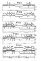
- FIG. 1 shows the cross section through an n-channel and p-channel transistor at this point in time.
- the reference numeral 1 denotes the p-doped silicon substrate, 2 the n-well for the p-channel transistor, and 3 the field oxide separating the active transistor regions, 4 and 5 the channel implantation, 6 the gate oxide and 7 and 8 the structured gate electrodes.
- Figure 2 After performing the n ⁇ -connection implantation with phosphorus ions to produce the low-doped connection area 9 of the LDD-n-channel transistor with the dose and energy of 1 - 2 x 1013 cm ⁇ 2 and 80 keV is the whole area by deposition from the gas phase (CVD) a 200 nm thick SiO2 layer (10a, 10b) applied; the layer thickness of this SiO2 layer (10a, 10b) of the flank oxide width of the gates 7, 8 is adapted. Through anisotropic etching back of the entire surface of the CVD-SiO2 layer, the flank oxide layers 10a and 10b (1st spacer) then arise at the gates 7 and 8 as etching residues.
- CVD gas phase
- the etching process is carried out by reactive ion etching in a mixture of trifluoromethane and oxygen.
- a reoxidation process is then carried out, a 30 nm thick SiO 2 layer 16 being formed on the silicon substrate (1, 4, 5, 9) and an 80 nm thick oxide layer 17, 18 being formed on the tantalum silicide of gates 7 and 8.
- CVD c hemical v apor d eposition
- FIG. 4 After covering the p-channel region with a first photoresist mask 12, the n + source / drain implantation is used to generate the source-drain regions 13 of the n-channel transistors with arsenic ions and a dose and energy of 6 x 1015 cm ⁇ 2 and 80 keV performed. After removing the photoresist mask 12, the source / drain regions 13 are activated at 900 ° C. in a nitrogen atmosphere in 60 minutes.
- the amorphous silicon spacers 11a, 11b are removed by, for example, a wet chemical etching process in a hydrofluoric acid / nitric acid mixture and then using a second photoresist mask which covers the n-channel regions (not shown), in a known manner by boron Ion implantation at a dose and energy of 4 x 1015 cm ⁇ 2 and 25 keV generated the source / drain regions 14 of the p-channel transistors. Finally (after removal of the second photoresist mask), the deposition of an SiO2 intermediate layer 15 and the completion of the arrangement (contact hole areas, metallization) are carried out in a known manner. The activation of the source / drain regions 14 takes place together with the flowing of the SiO2 intermediate layer 15 at 900 ° C in a nitrogen atmosphere in 40 minutes.
- the method according to the invention enables the n+ or p+ source / drain diffusion regions (13, 14) to be set back differently from the respective gate edge (7, 8).
- n-channel transistor is the Dielectric strength a return of the n+ implantation by approx. 0.35 ⁇ m from the gate edge is desired, while with the p-channel transistor 0.2 ⁇ m should not be exceeded in order to ensure a safe connection to the channel area. This requirement can easily be met by the method according to the invention, as just described.
Landscapes
- Metal-Oxide And Bipolar Metal-Oxide Semiconductor Integrated Circuits (AREA)
- Insulated Gate Type Field-Effect Transistor (AREA)
- Thin Film Transistor (AREA)
Applications Claiming Priority (2)
| Application Number | Priority Date | Filing Date | Title |
|---|---|---|---|
| DE3611758 | 1986-04-08 | ||
| DE3611758 | 1986-04-08 |
Publications (2)
| Publication Number | Publication Date |
|---|---|
| EP0240781A2 true EP0240781A2 (fr) | 1987-10-14 |
| EP0240781A3 EP0240781A3 (fr) | 1989-12-06 |
Family
ID=6298211
Family Applications (1)
| Application Number | Title | Priority Date | Filing Date |
|---|---|---|---|
| EP87103847A Withdrawn EP0240781A3 (fr) | 1986-04-08 | 1987-03-17 | Procédé pour la fabrication de masquage de flancs d'électrodes de grilles dans des transistors MOS ayant des zones de raccords de drains faiblement dopées |
Country Status (3)
| Country | Link |
|---|---|
| EP (1) | EP0240781A3 (fr) |
| JP (1) | JPS62242367A (fr) |
| KR (1) | KR870010636A (fr) |
Cited By (7)
| Publication number | Priority date | Publication date | Assignee | Title |
|---|---|---|---|---|
| EP0322665A3 (en) * | 1987-12-21 | 1990-02-14 | Sgs-Thomson Microelectronics S.R.L. | Process for manufacturing cmos integrated devices with reduced gate lengths |
| EP0329047A3 (en) * | 1988-02-12 | 1990-10-10 | Hitachi, Ltd. | Mis device with auxiliary gate and manufacturing method thereof |
| US5001073A (en) * | 1990-07-16 | 1991-03-19 | Sprague Electric Company | Method for making bipolar/CMOS IC with isolated vertical PNP |
| US5460993A (en) * | 1995-04-03 | 1995-10-24 | Taiwan Semiconductor Manufacturing Company Ltd. | Method of making NMOS and PMOS LDD transistors utilizing thinned sidewall spacers |
| US5547885A (en) * | 1990-04-03 | 1996-08-20 | Mitsubishi Denki Kabushiki Kaisha | Method of making asymmetric LDD transistor |
| CN116230755A (zh) * | 2023-05-05 | 2023-06-06 | 合肥晶合集成电路股份有限公司 | 一种半导体结构及其制作方法 |
| CN117613005A (zh) * | 2024-01-23 | 2024-02-27 | 中国科学院长春光学精密机械与物理研究所 | 一种混合型cmos器件及其制作方法 |
Family Cites Families (4)
| Publication number | Priority date | Publication date | Assignee | Title |
|---|---|---|---|---|
| JPS584975A (ja) * | 1981-06-30 | 1983-01-12 | Fujitsu Ltd | 半導体装置の製造方法 |
| DE3314450A1 (de) * | 1983-04-21 | 1984-10-25 | Siemens AG, 1000 Berlin und 8000 München | Verfahren zum herstellen von hochintegrierten komplementaeren mos-feldeffekttransistorschaltungen |
| US4577391A (en) * | 1984-07-27 | 1986-03-25 | Monolithic Memories, Inc. | Method of manufacturing CMOS devices |
| DE3530065C2 (de) * | 1984-08-22 | 1999-11-18 | Mitsubishi Electric Corp | Verfahren zur Herstellung eines Halbleiters |
-
1987
- 1987-03-17 EP EP87103847A patent/EP0240781A3/fr not_active Withdrawn
- 1987-04-03 JP JP62082760A patent/JPS62242367A/ja active Pending
- 1987-04-08 KR KR870003330A patent/KR870010636A/ko not_active Withdrawn
Cited By (10)
| Publication number | Priority date | Publication date | Assignee | Title |
|---|---|---|---|---|
| EP0322665A3 (en) * | 1987-12-21 | 1990-02-14 | Sgs-Thomson Microelectronics S.R.L. | Process for manufacturing cmos integrated devices with reduced gate lengths |
| EP0329047A3 (en) * | 1988-02-12 | 1990-10-10 | Hitachi, Ltd. | Mis device with auxiliary gate and manufacturing method thereof |
| US5547885A (en) * | 1990-04-03 | 1996-08-20 | Mitsubishi Denki Kabushiki Kaisha | Method of making asymmetric LDD transistor |
| US5849616A (en) * | 1990-04-03 | 1998-12-15 | Mitsubishi Denki Kabushiki Kaisha | Method of manufacturing a semiconductor device |
| US5001073A (en) * | 1990-07-16 | 1991-03-19 | Sprague Electric Company | Method for making bipolar/CMOS IC with isolated vertical PNP |
| US5460993A (en) * | 1995-04-03 | 1995-10-24 | Taiwan Semiconductor Manufacturing Company Ltd. | Method of making NMOS and PMOS LDD transistors utilizing thinned sidewall spacers |
| CN116230755A (zh) * | 2023-05-05 | 2023-06-06 | 合肥晶合集成电路股份有限公司 | 一种半导体结构及其制作方法 |
| CN116230755B (zh) * | 2023-05-05 | 2023-09-12 | 合肥晶合集成电路股份有限公司 | 一种半导体结构及其制作方法 |
| CN117613005A (zh) * | 2024-01-23 | 2024-02-27 | 中国科学院长春光学精密机械与物理研究所 | 一种混合型cmos器件及其制作方法 |
| CN117613005B (zh) * | 2024-01-23 | 2024-04-26 | 中国科学院长春光学精密机械与物理研究所 | 一种混合型cmos器件及其制作方法 |
Also Published As
| Publication number | Publication date |
|---|---|
| EP0240781A3 (fr) | 1989-12-06 |
| JPS62242367A (ja) | 1987-10-22 |
| KR870010636A (ko) | 1987-11-30 |
Similar Documents
| Publication | Publication Date | Title |
|---|---|---|
| DE69132695T2 (de) | CMOS-Verfahren mit Verwendung von zeitweilig angebrachten Siliciumnitrid-Spacern zum Herstellen von Transistoren (LDD) mit leicht dotiertem Drain | |
| EP0244607B1 (fr) | Méthode pour fabriquer des transistors CMOS optimisés à effet de champ en technologie VLSI | |
| DE3689158T2 (de) | Verfahren zum Herstellen bezüglich einer Karte justierten, implantierten Gebieten und Elektroden dafür. | |
| EP0226892B1 (fr) | Procédé pour la fabrication de transistors bipolaires et MOS-complémentaires sur un substrat commun en silicium | |
| DE69522992T2 (de) | Verfahren zur Herstellung eines Widerstands | |
| DE69835203T2 (de) | Herstellungsverfahren für nmos und pmos bauelemente mit reduzierte maskierungsschritten | |
| DE3019850C2 (fr) | ||
| DE69032735T2 (de) | Verfahren zum Herstellen von Hochspannungs- und Niederspannungs-CMOS-Transistoren in einem einzigen integrierten Schaltungs-Chip | |
| EP0839386B1 (fr) | Procede de fabrication d'un transistor mos | |
| DE4224793C2 (de) | Dünnfilmfeldeffektelement und Herstellungsverfahren dafür | |
| EP0123182B1 (fr) | Procédé pour la fabrication de circuits intégrés à haute densité comportant des transistors à effet de champ du type MOS complémentaires | |
| DE69130624T2 (de) | Verfahren zum Herstellen von Feldeffekt-Transistoren für integrierte Schaltungen | |
| EP0256315A1 (fr) | Circuit intégré contenant des transistors bipolaires et de type CMOS sur le même substrat et son procédé de fabrication | |
| DE3688057T2 (de) | Halbleitervorrichtung und Methode zur Herstellung. | |
| EP0248988A1 (fr) | Procédé pour fabriquer des circuits à transistors complémentaires à effet de champ du type MOS à haute intégration | |
| EP0118709A2 (fr) | Procédé pour la fabrication de transistor MOS à régions de source et drain planaires, à courte longueur de canal et à niveau de contact auto-aligné comportant un siliciure métallique | |
| DE3786785T2 (de) | Verfahren zur herstellung von mos-bauelementen für integrierte schaltungen. | |
| DE2845460A1 (de) | Verfahren zur herstellung einer halbleitervorrichtung | |
| EP0232497B1 (fr) | Procédé pour la fabrication simultanée de transistors bipolaires et MOS-complémentaires sur un substrat commun en silicium | |
| EP0224199A1 (fr) | Procédé pour fabriquer des circuits très intégrés comportant des transistors du type MOS à canal P et à canal N avec des électrodes à grille comportant une couche dopée double en polysilicium et siliciure métallique | |
| DE3788120T2 (de) | Verfahren zur herstellung gestapelter mos-strukturen. | |
| DE69133446T2 (de) | BiCMOS-Verfahren mit Bipolartransistor mit geringem Basis-Rekombinationsstrom | |
| EP0157926B1 (fr) | Procédé pour fabriquer un circuit intégré à transistors à effet de champ MOS à haute densité | |
| EP0159617B1 (fr) | Procédé pour fabriquer des transistors à effet de champ du type MOS à haute intégration | |
| DE2814695A1 (de) | Verfahren zum herstellen einer integrierten schaltung |
Legal Events
| Date | Code | Title | Description |
|---|---|---|---|
| PUAI | Public reference made under article 153(3) epc to a published international application that has entered the european phase |
Free format text: ORIGINAL CODE: 0009012 |
|
| AK | Designated contracting states |
Kind code of ref document: A2 Designated state(s): AT DE FR GB IT NL |
|
| PUAL | Search report despatched |
Free format text: ORIGINAL CODE: 0009013 |
|
| AK | Designated contracting states |
Kind code of ref document: A3 Designated state(s): AT DE FR GB IT NL |
|
| STAA | Information on the status of an ep patent application or granted ep patent |
Free format text: STATUS: THE APPLICATION IS DEEMED TO BE WITHDRAWN |
|
| 18D | Application deemed to be withdrawn |
Effective date: 19891001 |
|
| RIN1 | Information on inventor provided before grant (corrected) |
Inventor name: ENDERS, GERHARD, DIPL.-PHYS. Inventor name: MOHR, ERNST-GUENTHER, DIPL.-PHYS. |