EP0241219A2 - Pièce d'horlogerie électronique - Google Patents
Pièce d'horlogerie électronique Download PDFInfo
- Publication number
- EP0241219A2 EP0241219A2 EP87302878A EP87302878A EP0241219A2 EP 0241219 A2 EP0241219 A2 EP 0241219A2 EP 87302878 A EP87302878 A EP 87302878A EP 87302878 A EP87302878 A EP 87302878A EP 0241219 A2 EP0241219 A2 EP 0241219A2
- Authority
- EP
- European Patent Office
- Prior art keywords
- voltage
- electronic timepiece
- capacitor
- circuit
- step motor
- Prior art date
- Legal status (The legal status is an assumption and is not a legal conclusion. Google has not performed a legal analysis and makes no representation as to the accuracy of the status listed.)
- Granted
Links
Images


Classifications
-
- G—PHYSICS
- G04—HOROLOGY
- G04C—ELECTROMECHANICAL CLOCKS OR WATCHES
- G04C10/00—Arrangements of electric power supplies in time-pieces
Definitions
- This invention relates to electronic timepieces and in particular, although not so restricted, to electronic timepieces with a charging function in which solar cells or generators serve as power sources.
- a rechargable electronic timepiece which has a primary power source such as a solar cell or a manually operated generator, and a secondary power source such as a plurality of capacitors having different capacitancies.
- One conventional electronic timepiece of this type has a capacitor with a relatively large capacitance which, when fully charged, is capable of driving the electronic timepiece for several days, a capacitor with a relatively small capacitance which can be instantaneously charged to produce a relatively large voltage but which is capable of driving the electronic timepiece for only several seconds, and a charge control circuit which connects or disconnects the primary power source with the secondary power source by detecting terminal voltages of both capacitors.
- the conventional rechargable electronic timepiece as described above has the following disadvantages.
- Time intervals for detecting the terminal voltage are the same for the relatively small capacitance capacitor and the relatively large capacitance capacitor.
- capacitors having as small a capacitance as possible in order to shorten the time for initiating operation of the electronic timepiece.
- a primary power source which is capable of rapidly generating electricity, such as a manually operated generator. In this case, if the voltage detecting period is long, the current supply path is not properly switched, and the relatively small capacitance capacitor loses performance, or in the worst case breaks down, due to being charged to a voltage in excess of its maximum rating voltage.
- the charge control circuit has a relatively large number of circuit elements since a plurality of voltage levels have to be detected for each capacitor and the same voltage cannot be detected since different voltage driving impedance elements have to be provided for each of the voltages to be detected.
- an electronic timepiece characterised by comprising: oscillator means for generating a time base signal; frequency dividing means for frequency dividing the time base signal; pulse synthesising circuit means for producing a plurality of control signals in response to a signal from said frequency dividing means; a step motor driving means for generating and controlling driving pulses for a step motor in response to the control signals of said pulse synthesising circuit means; power supply means for generating, storing and supplying electric energy; voltage detecting means for detecting a plurality of voltage levels of said power supply means; and charge control means for controlling storage and supply of electric energy in and from said power supply means in response to the result of detection of said voltage detecting means.
- said power supply means comprises a primary power source for generating electric energy, and a secondary power source for storing said electric energy and comprising a first capacitor having a relatively large capacitance, and a second capacitor having a relatively small capacitance.
- said voltage detecting means comprises a sampling signal selecting circuit for producing sampling signals of different periods depending upon the result of voltage detection, and a plurality of voltage detectors for detecting a plurality of voltage levels of said first capacitor and said second capacitor, respectively.
- Said sampling signal selecting circuit may be arranged to produce a first sampling signal having a relatively short period when the electronic timepiece is powered by said second capacitor, and produces a second sampling signal having a relatively long period when the electronic timepiece is powered by said first capacitor.
- each voltage detector comprises a plurality of switching elements for selecting the voltage to be detected, and a voltage comparator for comparing said selected voltage with a reference voltage.
- said step motor driving means is arranged to generate driving pulses to effect different manners of movement of a time indicating member in dependence upon the result of voltage detection.
- said step motor driving means may be arranged to generate a first driving pulse for normal movement of said time indicating member when the electronic timepiece is powered by said first capacitor and to generate a second driving pulse for abnormal movement different from the normal movement of said time indicating member when the electronic timepiece is powered by said second capacitor.
- the electronic timepiece is provided with first reset means for resetting, in response to an external operation, said step motor driving means but not said oscillator means and said frequency dividing means and a second reset means for resetting at least said frequency dividing means for a relatively short time after a reset condition of the first reset means has been released.
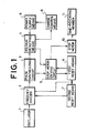
- the electronic timepiece has an oscillator 1 which oscillates at, for example, 32768 Hz, a frequency divider 2 which divides the frequency of the output of the oscillator circuit 1, a pulse synthesising circuit 3 which receives suitable signals from the frequency divider 2, a voltage detecting means 4 which receives a sampling signal from the pulse synthesising circuit 3 and which detects the voltage of a plurality of capacitors contained in a power supply means 9.
- An output of the voltage detecting means 4 is connected to a charge control means 6 and to a step motor driving circuit 5.
- the charge control means 6 receives the output of the voltage detecting means and controls a switching operation of charge/discharge states of the capacitors.
- the step motor driving circuit 5 receives an output from the voltage detecting means 4 and an output from the pulse synthesising circuit 3, and sends a driving signal to a step motor 10.
- the step motor 10 drives a time indicating member 11 such as hours, minutes and seconds hands.
- a first reset means 8 stops the drive signal from being generated under a reset condition determined by external operation, and a second reset means 7 resets the frequency divider 2 for a short period of time after the reset condition has been released.
- FIG. 2 is a diagram showing the states of the charge control means 6, wherein symbol GEN denotes a generating means such as a solar cell or manually operated generator, C1 denotes an electric double layer capacitor having a relatively large capacitance, for example, 0.33F and C2 denotes a tantalum capacitor having a relatively small capacitance of, for example, 6.8 micro F. Symbols D2 and D3 denote reverse current preventing diodes, and symbol D1 denotes a diode that is contained in the generator means. Symbols S1, S2 and S3 denote switches for changing a loop for electric charge/discharge states. Symbol VC1 denotes a voltage on the capacitor C1, VC2 denotes a voltage on the capacitor C2 and VDD and VSS denote voltages with which the power supply means 9 drives a logic circuit 20 which comprises the circuits of Figure 1.
- GEN denotes a generating means such as a solar cell or manually operated generator
- C1 denotes an electric double layer
- VSD and VSB denote anode voltage and cathode voltage respectively of the diode D2.
- VOP1 is defined as a voltage at which the logic circuit 20 operates
- VSTP is defined as a minimum operable voltage of the logic circuit 20
- VOP2 is defined as: VSTP ⁇ VOP2 ⁇ VOP1
- VFUL denotes a maximum rating voltage of the capacitors.
- a state (A) shows the state under the condition of VC1 ⁇ VOP2 and VC2 ⁇ VOP2.
- the switches S1, S2 and S3 are all turned off, and electric current generated from the generating means GEN is supplied to the logic circuit 20 through a loop "a". Therefore, the capacitor C2 is electrically charged immediately.
- state (A) the voltage VC2 is detected. If VC2 > VOP1, state (A) changes to state (B).
- state (B) the switches S1 and S3 are turned off, and the switch S2 is turned on.
- the generating means GEN and the capacitor C1 are independently connected, and the electric current from the generating means GEN charges the capacitor C1 through a path "b".
- a voltage VC2 is applied to the logic circuit 20 and a discharge current flows from the capacitor C2 through the path "b".
- state (B) the voltage VC2 is detected. If VC2 ⁇ VOP2, state (B) returns to state (A). The voltage VC1 is also detected in state (B). If VC1 > VOP1, this state changes to a state (C).
- the time indicating hands are moved in the states (A) and (B) in a manner different from normal movement.
- state (C) of Figure 2 the switches S1 and S2 are turned on, and the switch S3 is turned off. This is a normally used condition where the capacitors C1 and C2 are connected in parallel with the generating means GEN to supply the logic circuit 20. If VC1 ⁇ VSTP, this state returns to state (A). Further, if VC1 > VFUL, this state changes to state (D). In state (D), the switches S1, S2 and S3 are turned on. With the switch S3 turned on, a voltage greater than VFUL is not applied to the capacitor C1 to prevent overcharging. In this case, the voltage of the capacitor C1 is supplied to the logic circuit 20. If the voltage VC1 of the capacitor C1 becomes smaller than VFUL, this state returns to state (C). In states (C) and (D), the time indicating hands are moved normally each second.
- Figure 3 illustrates the voltage detecting means 4 and the charge control means 6, which enable the charge/discharge states of Figure 2 to be changed.
- the voltage detecting means 4 consists of a voltage detecting circuit 25 and a control circuit.
- the charge control means 6 consists of MOS transistors switches S1, S2 and S3.
- a voltage detecting output 27 detects VSTP and VC1.
- the voltage detecting output 27 assumes "L” level, and the output of an inverter 32 assumes "H” level, whereby a latch circuit constituted by NOR gates 33 and 34 is reset, and switches S1 and S2 are turned off in response to the output of inverters 37,38 and inverters 41,42.
- This operation means that state (C) of Figure 2 is changed to state (A).
- a voltage detecting output 28 detects VOP2 and VC2.
- VOP2 When VC2 ⁇ VOP2, the voltage detecting output 27 assumes "L" level, whereby a latch circuit constituted by NOR gates 39 and 40 is reset, and the switch S2 is turned off in response to the output of the inverter 42.
- This operation means that state (B) of Figure 2 is changed to state (A).
- state (C) In state (C), however, the NOR gate 33 produces an output of "H” level, so the switch S2 is not turned off.
- a voltage detecting output 29 detects VOP1 and VC2.
- VOP1 the voltage detecting output 29 assumes "H" level, whereby the latch circuit constituted by NOR gates 39 and 40 is set, and the switch S2 is turned on. This operation means that state (A) of Figure 2 is changed to state (B).
- a voltage detecting output 30 detects VOP1 and VC1.
- VOP1 the voltage detecting output 30 assumes "H" level, whereby the latch circuit constituted by NOR gates 33 and 34 is set, and the switch S1 is turned on. This operation means that state (B) shown in Figure 2 is changed to state (C).
- a voltage detecting output 31 detects VFUL and VC1.
- the voltage detecting output 31 assumes "H” level and the output of an inverter 43 assumes “L” level, whereby the switch S3 is turned on.
- the switch S3 is turned off. This operation means that state (C) of Figure 2 is changed to state (D), or vice versa.
- the voltage detecting circuit 25 comprises five voltage detectors. Sampling signals SP1, SP2, SP3, SP4 and SP5 for these voltage detectors are supplied by the pulse synthesising circuit 3, and a control signal SF selects a frequency of the sampling signals SP2 and SP3 which are used for detecting the voltage VC2 of the capacitor C2.
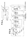
- FIG. 4 is a simple circuit diagram which shows an example of a sampling signal selecting circuit 12 which is comprised of two AND gates 15,16 which receive the control signal SF and signals of 1Hz and 1KHz sent from the frequency divider 2, and an OR gate 17 which receives outputs of the AND gates 15,16 and which produces the sampling signal SP2 or SP3.
- control signal SF assumes "L" level so long as a condition VC2 ⁇ VOP1 is maintained.
- Figure 5 concretely illustrates the first reset means 8 and the second reset means 7 and Figure 6 is a timing chart illustrating their operation.
- a reset terminal 49 assumes "H" level and data is read through a chattering-preventing circuit which is constituted by flip-flops 53, 54, 55, 56 and 57. As shown in Figure 6, to read the data a minimum time of 7.32 msec and a maximum time of 11.23 msec is required.
- the flip-flop 55 produces an output of level "H"
- the step motor driving circuit 5 is reset to stop the driving signal from being generated. Since the first reset means 8 does not reset the frequency divider 2, the voltage detecting means 4 operates in its ordinary manner.
- the second reset means 7 produces a one-shot pulse of a width of 0.49 msec after the reset condition is released.
- the one-shot pulse is produced by a NOR gate 58 after a time of 0.98 msec has elapsed at the longest from release of the reset condition.
- a frequency dividing stage of the frequency divider 2 subsequent to 512Hz is reset, and the driving signal is produced after about one second has elapsed.
- an input RIS is sent from the step motor driving circuit 5, and denotes an inhibition signal for resetting operation when the driving signal is produced.
- FIG. 7 shows a voltage detector for detecting VC2 > VOP1 and VC1 > VOP1 in the voltage detecting circuit 25 in Figure 3.
- each voltage detector consists of impedance elements which divide the voltage VC1 or VC2 according to each detecting voltage level, and a voltage comparator which compares the divided voltage VDIV with a reference voltage VREF produced by a voltage reference 61.
- the voltage VOP1 is compared with voltages VC1 and VC2 so that impedance elements Z1,Z2 and a voltage comparator 60 are used for both voltages VC1 and VC2.
- switching elements TR1 and TR2 which select the voltage VC1 or VC2 to be detected, and AND gates 62,63 which select the output of the voltage comparator 60 are provided.
- the sampling signal SP3 or SP4 produced from the pulse synthesising circuit 3 turns the switching element TR1 or TR2 on, and the terminal voltage VC1 or VC2 to be detected is divided by the impedance elements Z1 and Z2.
- the resulting divided voltage VDIV is compared by the voltage comparator 60 with the reference voltage VREF, and the compared result is produced as a signal OUT.
- the voltage detecting output 29 or 30 is produced by the AND gate 62 or 63 in accordance with the sampling signal SP3 or SP4.
- VDIV(SP3) VC2 ⁇ Z1/(Z1 + Z2)
- the comparator 60 compares the reference voltage VREF with the divided output VDIV, and produces the result as the signal OUT. Therefore, the condition in which the signal OUT assumes "H" level is given by, VC1 > VREF ⁇ (Z1 + Z2)/Z1 VC2 > VREF ⁇ (Z1 + Z2)/Z1
- the signal OUT operates in sections T1, T2 and T3 as follows:
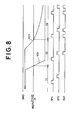
- Figure 9 illustrates the relationship between the voltage VC1 and the movement of the timekeeping hands wherein the charging operation is continued from when the voltage VC1 of the capacitor C1 is zero volts to when it reaches VFUL, and after the moment the charging operation is stopped.
- the state (A) or state (B) in Figure 2 is established from 0V to VOP1; during this period the step motor is driven by the voltage VC2.
- the seconds hand is moved every two seconds to warn that the electronic timepiece will cease to operate soon if the charging operation is not carried out.
- state (C) is established where the step motor is driven by the voltage VC1, and the seconds hand moves normally every second.
- state (D) As the voltage VC1 reaches VFUL, state (D) is established, and the voltage VC1 is clamped. If the charging operation is stopped at this moment, the voltage VC1 gradually decreases due to discharge of electricity and the seconds hand is moved normally every second until the voltage VC1 falls to VOP2. If the voltage VC1 becomes smaller than VOP2, the seconds hand is moved again every two seconds to warn that the voltage VC1 is low. If the voltage VC1 falls below VSTP, state (A) is resumed. If a charging operation is still not carried out, the electronic timepiece ceases to operate.
- the seconds hand is moved every two seconds over a range of the voltage VC1 from 0V to VOP1
- the charge control means is provided with a voltage sampling signal selecting circuit, and the period for detecting the voltage on the capacitors is varied depending upon the terminal voltage of the capacitor, so that the relatively small capacitance capacitor is not impressed with a voltage greater than its maximum rating voltage and so that it will not lose performance or break down.
- the first reset means and the second reset means allows the charge/discharge operation to continue irrespective of the reset condition or non-reset condition, and without requiring any additional element.
- the electronic timepiece While the electronic timepiece is powered by the small capacitance capacitor only, the time indicating hands are moved in a manner different from their normal movement thereby indicating that the capacitor is being electrically charged. This helps solve the problem of the electronic timepiece ceasing to operate while the user is unaware of the fact that the capacitor needs to be charged. Thus, the electronic timepiece can be used reliably.
- the voltage detecting circuit employs a reduced number of elements compared to that of conventional electronic timepieces to detect voltage. This allows a decrease in the number of parts of an electronic timepiece or reduction in size of parts, and, hence, a reduction in the size of the electronic timepiece as a whole and a decrease in manufacturing cost.
Landscapes
- Engineering & Computer Science (AREA)
- Power Engineering (AREA)
- Physics & Mathematics (AREA)
- General Physics & Mathematics (AREA)
- Electromechanical Clocks (AREA)
Applications Claiming Priority (8)
| Application Number | Priority Date | Filing Date | Title |
|---|---|---|---|
| JP61080724A JPS62236332A (ja) | 1986-04-08 | 1986-04-08 | 充電回路 |
| JP80717/86 | 1986-04-08 | ||
| JP80724/86 | 1986-04-08 | ||
| JP8071786A JPS62237382A (ja) | 1986-04-08 | 1986-04-08 | 電子時計の電圧検出回路 |
| JP61081517A JPS62238487A (ja) | 1986-04-09 | 1986-04-09 | 充電式電子時計 |
| JP81517/86 | 1986-04-09 | ||
| JP8656786A JPS62242882A (ja) | 1986-04-15 | 1986-04-15 | 電子時計 |
| JP86567/86 | 1986-04-15 |
Publications (3)
| Publication Number | Publication Date |
|---|---|
| EP0241219A2 true EP0241219A2 (fr) | 1987-10-14 |
| EP0241219A3 EP0241219A3 (en) | 1989-12-06 |
| EP0241219B1 EP0241219B1 (fr) | 1993-01-13 |
Family
ID=27466469
Family Applications (1)
| Application Number | Title | Priority Date | Filing Date |
|---|---|---|---|
| EP87302878A Expired - Lifetime EP0241219B1 (fr) | 1986-04-08 | 1987-04-02 | Pièce d'horlogerie électronique |
Country Status (3)
| Country | Link |
|---|---|
| US (1) | US4785435A (fr) |
| EP (1) | EP0241219B1 (fr) |
| DE (1) | DE3783499T2 (fr) |
Cited By (9)
| Publication number | Priority date | Publication date | Assignee | Title |
|---|---|---|---|---|
| EP0326313A3 (fr) * | 1988-01-25 | 1991-03-20 | Seiko Epson Corporation | Montre bracelet |
| EP0695978A1 (fr) | 1994-08-03 | 1996-02-07 | Seiko Instruments Inc. | Montre de contrÔle électronique |
| EP0701184A4 (fr) * | 1994-03-29 | 1996-08-21 | Citizen Watch Co Ltd | Dispositif d'alimentation en energie pour appareils electriques |
| EP0898355A3 (fr) * | 1997-07-22 | 1999-11-24 | Seiko Instruments R&D Center Inc. | Appareil électronique |
| EP0961183A4 (fr) * | 1997-12-11 | 2000-01-19 | Citizen Watch Co Ltd | Dispositif electronique de mesure du temps |
| EP0903649A4 (fr) * | 1997-02-06 | 2002-05-02 | Citizen Watch Co Ltd | Horloge electronique |
| EP1542099A4 (fr) * | 2002-09-19 | 2010-09-08 | Citizen Holdings Co Ltd | Horloge electronique |
| EP2219084A3 (fr) * | 2009-01-16 | 2010-10-06 | Casio Computer Co., Ltd. | Horloge électronique |
| EP2202591A3 (fr) * | 2008-12-26 | 2010-10-06 | Casio Computer Co., Ltd. | Pièce d'horlogerie électronique |
Families Citing this family (15)
| Publication number | Priority date | Publication date | Assignee | Title |
|---|---|---|---|---|
| DE69511649T2 (de) * | 1994-04-06 | 2000-04-06 | Citizen Watch Co., Ltd. | Elektronische uhr |
| DE19700108B4 (de) * | 1997-01-03 | 2005-12-22 | Citizen Watch Co., Ltd. | Elektronische Uhr und Ladeverfahren derselben |
| US6034492A (en) * | 1997-04-30 | 2000-03-07 | Nec Corporation | Motor-generator |
| DE69939249D1 (de) * | 1998-09-22 | 2008-09-18 | Seiko Epson Corp | Elektronische uhr sowie verfahren zur energieversorgung und zeiteinstellung dafür |
| JP3678075B2 (ja) * | 1998-12-09 | 2005-08-03 | セイコーエプソン株式会社 | 電源装置およびその制御方法、携帯型電子機器、計時装置およびその制御方法 |
| JP2000323695A (ja) * | 1999-05-14 | 2000-11-24 | Nec Corp | 固体撮像素子およびその製造方法 |
| ITMI20070453A1 (it) * | 2007-03-07 | 2008-09-08 | Korotek S R L | Metodo e dispositivo di autenticazione dell'identita' in grado di generare codici di acesso univoci tramite la decodifica di immagini la cui luce e'inoltre utilizzata per l'alimentazione del dispositivo stesso |
| US7898439B2 (en) * | 2008-03-20 | 2011-03-01 | Isabelle Bettez | Bicycle rental system and station |
| JP2012078343A (ja) * | 2010-09-08 | 2012-04-19 | Seiko Instruments Inc | 駆動制御装置、時計装置、及び電子機器 |
| US9176636B1 (en) | 2014-10-22 | 2015-11-03 | Cypress Semiconductor Corporation | Low power capacitive sensor button |
| USD774237S1 (en) | 2015-05-07 | 2016-12-13 | Kenall Manufacturing Company | Lighting fixture |
| EP3432088A1 (fr) * | 2017-07-17 | 2019-01-23 | The Swatch Group Research and Development Ltd | Pièce d'horlogerie électromécanique |
| US10800378B1 (en) | 2020-02-21 | 2020-10-13 | Lyft, Inc. | Vehicle docking stations heartbeat and security |
| US12209437B2 (en) | 2020-12-11 | 2025-01-28 | Lyft, Inc. | Docking station for micromobility transit vehicles |
| JP2024127047A (ja) * | 2023-03-08 | 2024-09-20 | セイコーエプソン株式会社 | 電子制御式機械時計 |
Family Cites Families (4)
| Publication number | Priority date | Publication date | Assignee | Title |
|---|---|---|---|---|
| JPH0792506B2 (ja) * | 1984-11-21 | 1995-10-09 | セイコーエプソン株式会社 | 電子時計 |
| US4634953A (en) * | 1984-04-27 | 1987-01-06 | Casio Computer Co., Ltd. | Electronic equipment with solar cell |
| JPS61202186A (ja) * | 1985-03-05 | 1986-09-06 | Seiko Instr & Electronics Ltd | 電子時計 |
| JPH10784A (ja) * | 1996-06-13 | 1998-01-06 | Brother Ind Ltd | インクカートリッジ |
-
1987
- 1987-04-02 EP EP87302878A patent/EP0241219B1/fr not_active Expired - Lifetime
- 1987-04-02 DE DE8787302878T patent/DE3783499T2/de not_active Expired - Lifetime
- 1987-04-06 US US07/035,087 patent/US4785435A/en not_active Expired - Lifetime
Cited By (16)
| Publication number | Priority date | Publication date | Assignee | Title |
|---|---|---|---|---|
| EP0326313A3 (fr) * | 1988-01-25 | 1991-03-20 | Seiko Epson Corporation | Montre bracelet |
| EP0701184A4 (fr) * | 1994-03-29 | 1996-08-21 | Citizen Watch Co Ltd | Dispositif d'alimentation en energie pour appareils electriques |
| EP0695978B1 (fr) * | 1994-08-03 | 2001-12-12 | Seiko Instruments Inc. | Montre de contrôle électronique |
| EP0695978A1 (fr) | 1994-08-03 | 1996-02-07 | Seiko Instruments Inc. | Montre de contrÔle électronique |
| EP0982638A1 (fr) | 1994-08-03 | 2000-03-01 | Seiko Instruments Inc. | Montre de contrôle électronique |
| EP0903649A4 (fr) * | 1997-02-06 | 2002-05-02 | Citizen Watch Co Ltd | Horloge electronique |
| EP0898355A3 (fr) * | 1997-07-22 | 1999-11-24 | Seiko Instruments R&D Center Inc. | Appareil électronique |
| US6122185A (en) * | 1997-07-22 | 2000-09-19 | Seiko Instruments R&D Center Inc. | Electronic apparatus |
| EP0961183A4 (fr) * | 1997-12-11 | 2000-01-19 | Citizen Watch Co Ltd | Dispositif electronique de mesure du temps |
| US6301198B1 (en) | 1997-12-11 | 2001-10-09 | Citizen Watch Co., Ltd. | Electronic timepiece |
| EP1542099A4 (fr) * | 2002-09-19 | 2010-09-08 | Citizen Holdings Co Ltd | Horloge electronique |
| EP2202591A3 (fr) * | 2008-12-26 | 2010-10-06 | Casio Computer Co., Ltd. | Pièce d'horlogerie électronique |
| US8111590B2 (en) | 2008-12-26 | 2012-02-07 | Casio Computer Co., Ltd. | Electronic timepiece |
| CN101770204B (zh) * | 2008-12-26 | 2012-05-23 | 卡西欧计算机株式会社 | 电子表 |
| EP2219084A3 (fr) * | 2009-01-16 | 2010-10-06 | Casio Computer Co., Ltd. | Horloge électronique |
| CN101782740B (zh) * | 2009-01-16 | 2014-02-26 | 卡西欧计算机株式会社 | 电子钟表 |
Also Published As
| Publication number | Publication date |
|---|---|
| EP0241219B1 (fr) | 1993-01-13 |
| EP0241219A3 (en) | 1989-12-06 |
| DE3783499D1 (de) | 1993-02-25 |
| DE3783499T2 (de) | 1993-04-29 |
| US4785435A (en) | 1988-11-15 |
Similar Documents
| Publication | Publication Date | Title |
|---|---|---|
| EP0241219B1 (fr) | Pièce d'horlogerie électronique | |
| KR940006915B1 (ko) | 발전 장치 부착 전자 팔목시계 | |
| US4653931A (en) | Self-charging electronic timepiece | |
| US4730287A (en) | Power supply for electronic timpiece | |
| US5889734A (en) | Electronic timepiece | |
| KR100514448B1 (ko) | 전자 시계 | |
| US4702613A (en) | Electronic timepiece driven by a plurality of stepping motors and powered by a solar cell | |
| US20050030683A1 (en) | Self-reparable device to generate a high voltage, and method for repairing a device to generate a high voltage | |
| EP1026559B1 (fr) | Montre electronique ayant une fonction de generation d'electricite | |
| US6208119B1 (en) | Electronic speed-control circuit | |
| EP0241202B1 (fr) | Pièce d'horlogerie électronique et analogique à dispositif de charge | |
| US4785436A (en) | Photovoltaic electronic timepiece | |
| GB2158274A (en) | Electronic timepiece | |
| EP1542099B1 (fr) | Horloge électronique | |
| US6646960B1 (en) | Electronic timepiece | |
| US5798985A (en) | Electronic watch and method of driving the same | |
| KR100295768B1 (ko) | 전자시계 | |
| US6636459B1 (en) | Electronic clock and method of controlling the clock | |
| JP2870516B2 (ja) | 発電装置付電子時計 | |
| JP3624531B2 (ja) | 電力制御装置、発電装置および電子機器 | |
| JPH0481754B2 (fr) | ||
| JP3706622B2 (ja) | 太陽電池時計 | |
| JP3673318B2 (ja) | 充電式時計及び電源の供給方法 | |
| JPH0755961A (ja) | 太陽電池時計 | |
| JPH07117588B2 (ja) | 電子時計 |
Legal Events
| Date | Code | Title | Description |
|---|---|---|---|
| PUAI | Public reference made under article 153(3) epc to a published international application that has entered the european phase |
Free format text: ORIGINAL CODE: 0009012 |
|
| AK | Designated contracting states |
Kind code of ref document: A2 Designated state(s): CH DE GB LI |
|
| PUAL | Search report despatched |
Free format text: ORIGINAL CODE: 0009013 |
|
| AK | Designated contracting states |
Kind code of ref document: A3 Designated state(s): CH DE GB LI |
|
| 17P | Request for examination filed |
Effective date: 19900525 |
|
| 17Q | First examination report despatched |
Effective date: 19911206 |
|
| GRAA | (expected) grant |
Free format text: ORIGINAL CODE: 0009210 |
|
| AK | Designated contracting states |
Kind code of ref document: B1 Designated state(s): CH DE GB LI |
|
| REF | Corresponds to: |
Ref document number: 3783499 Country of ref document: DE Date of ref document: 19930225 |
|
| PLBI | Opposition filed |
Free format text: ORIGINAL CODE: 0009260 |
|
| 26 | Opposition filed |
Opponent name: JUNGHANS UHREN GMBH Effective date: 19931009 |
|
| REG | Reference to a national code |
Ref country code: GB Ref legal event code: 746 Effective date: 19950502 |
|
| APAC | Appeal dossier modified |
Free format text: ORIGINAL CODE: EPIDOS NOAPO |
|
| PLBN | Opposition rejected |
Free format text: ORIGINAL CODE: 0009273 |
|
| STAA | Information on the status of an ep patent application or granted ep patent |
Free format text: STATUS: OPPOSITION REJECTED |
|
| 27O | Opposition rejected |
Effective date: 19970618 |
|
| REG | Reference to a national code |
Ref country code: GB Ref legal event code: IF02 |
|
| APAH | Appeal reference modified |
Free format text: ORIGINAL CODE: EPIDOSCREFNO |
|
| PGFP | Annual fee paid to national office [announced via postgrant information from national office to epo] |
Ref country code: GB Payment date: 20060329 Year of fee payment: 20 Ref country code: CH Payment date: 20060329 Year of fee payment: 20 |
|
| PGFP | Annual fee paid to national office [announced via postgrant information from national office to epo] |
Ref country code: DE Payment date: 20060330 Year of fee payment: 20 |
|
| PG25 | Lapsed in a contracting state [announced via postgrant information from national office to epo] |
Ref country code: GB Free format text: LAPSE BECAUSE OF EXPIRATION OF PROTECTION Effective date: 20070401 |
|
| REG | Reference to a national code |
Ref country code: GB Ref legal event code: PE20 |
|
| REG | Reference to a national code |
Ref country code: CH Ref legal event code: PL |