EP0242298A2 - Lawinen Fotodiode - Google Patents
Lawinen Fotodiode Download PDFInfo
- Publication number
- EP0242298A2 EP0242298A2 EP87400859A EP87400859A EP0242298A2 EP 0242298 A2 EP0242298 A2 EP 0242298A2 EP 87400859 A EP87400859 A EP 87400859A EP 87400859 A EP87400859 A EP 87400859A EP 0242298 A2 EP0242298 A2 EP 0242298A2
- Authority
- EP
- European Patent Office
- Prior art keywords
- layer
- light
- avalanche multiplication
- band gap
- gap energy
- Prior art date
- Legal status (The legal status is an assumption and is not a legal conclusion. Google has not performed a legal analysis and makes no representation as to the accuracy of the status listed.)
- Ceased
Links
Images

Classifications
-
- H—ELECTRICITY
- H10—SEMICONDUCTOR DEVICES; ELECTRIC SOLID-STATE DEVICES NOT OTHERWISE PROVIDED FOR
- H10F—INORGANIC SEMICONDUCTOR DEVICES SENSITIVE TO INFRARED RADIATION, LIGHT, ELECTROMAGNETIC RADIATION OF SHORTER WAVELENGTH OR CORPUSCULAR RADIATION
- H10F30/00—Individual radiation-sensitive semiconductor devices in which radiation controls the flow of current through the devices, e.g. photodetectors
- H10F30/20—Individual radiation-sensitive semiconductor devices in which radiation controls the flow of current through the devices, e.g. photodetectors the devices having potential barriers, e.g. phototransistors
- H10F30/21—Individual radiation-sensitive semiconductor devices in which radiation controls the flow of current through the devices, e.g. photodetectors the devices having potential barriers, e.g. phototransistors the devices being sensitive to infrared, visible or ultraviolet radiation
- H10F30/22—Individual radiation-sensitive semiconductor devices in which radiation controls the flow of current through the devices, e.g. photodetectors the devices having potential barriers, e.g. phototransistors the devices being sensitive to infrared, visible or ultraviolet radiation the devices having only one potential barrier, e.g. photodiodes
- H10F30/225—Individual radiation-sensitive semiconductor devices in which radiation controls the flow of current through the devices, e.g. photodetectors the devices having potential barriers, e.g. phototransistors the devices being sensitive to infrared, visible or ultraviolet radiation the devices having only one potential barrier, e.g. photodiodes the potential barrier working in avalanche mode, e.g. avalanche photodiodes
- H10F30/2255—Individual radiation-sensitive semiconductor devices in which radiation controls the flow of current through the devices, e.g. photodetectors the devices having potential barriers, e.g. phototransistors the devices being sensitive to infrared, visible or ultraviolet radiation the devices having only one potential barrier, e.g. photodiodes the potential barrier working in avalanche mode, e.g. avalanche photodiodes in which the active layers form heterostructures, e.g. SAM structures
-
- H—ELECTRICITY
- H10—SEMICONDUCTOR DEVICES; ELECTRIC SOLID-STATE DEVICES NOT OTHERWISE PROVIDED FOR
- H10F—INORGANIC SEMICONDUCTOR DEVICES SENSITIVE TO INFRARED RADIATION, LIGHT, ELECTROMAGNETIC RADIATION OF SHORTER WAVELENGTH OR CORPUSCULAR RADIATION
- H10F30/00—Individual radiation-sensitive semiconductor devices in which radiation controls the flow of current through the devices, e.g. photodetectors
- H10F30/20—Individual radiation-sensitive semiconductor devices in which radiation controls the flow of current through the devices, e.g. photodetectors the devices having potential barriers, e.g. phototransistors
- H10F30/21—Individual radiation-sensitive semiconductor devices in which radiation controls the flow of current through the devices, e.g. photodetectors the devices having potential barriers, e.g. phototransistors the devices being sensitive to infrared, visible or ultraviolet radiation
- H10F30/22—Individual radiation-sensitive semiconductor devices in which radiation controls the flow of current through the devices, e.g. photodetectors the devices having potential barriers, e.g. phototransistors the devices being sensitive to infrared, visible or ultraviolet radiation the devices having only one potential barrier, e.g. photodiodes
- H10F30/225—Individual radiation-sensitive semiconductor devices in which radiation controls the flow of current through the devices, e.g. photodetectors the devices having potential barriers, e.g. phototransistors the devices being sensitive to infrared, visible or ultraviolet radiation the devices having only one potential barrier, e.g. photodiodes the potential barrier working in avalanche mode, e.g. avalanche photodiodes
-
- H—ELECTRICITY
- H10—SEMICONDUCTOR DEVICES; ELECTRIC SOLID-STATE DEVICES NOT OTHERWISE PROVIDED FOR
- H10F—INORGANIC SEMICONDUCTOR DEVICES SENSITIVE TO INFRARED RADIATION, LIGHT, ELECTROMAGNETIC RADIATION OF SHORTER WAVELENGTH OR CORPUSCULAR RADIATION
- H10F77/00—Constructional details of devices covered by this subclass
- H10F77/10—Semiconductor bodies
- H10F77/12—Active materials
- H10F77/124—Active materials comprising only Group III-V materials, e.g. GaAs
- H10F77/1248—Active materials comprising only Group III-V materials, e.g. GaAs having three or more elements, e.g. GaAlAs, InGaAs or InGaAsP
Definitions
- This invention relates to a semiconductor avalanche photo-diode (referred to hereinafter as APD). More particularly, it relates to an APD having improved dark current, noise and high frequency characteristics by achieving uniform avalanche multiplication therein.
- APD semiconductor avalanche photo-diode
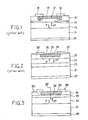
- an APD device composed of InP/GaInAs (Indium-Phosphorus/Galium-Indium-Arsenide) is generally used. Its structure is schematically shown in cross-sectional side view in Fig.1.
- a DC operating voltage of approximately 100 V is applied between a negative electrode 18 and a positive electrode 19.
- Numeral 11 denotes an n+-type InP substrate over which an n-type GaInAs light-absorbing layer 12 is formed, in which electrons and positive holes are excited by light injected thereinto.
- the mark “e” denotes an electron
- the mark “ph” denotes a positive hole both of which are produced by light excitation.
- the arrow marks indicate directions of their move under the applied operating voltage.
- Numeral 14 denotes a window layer, sometimes called a multiplication region, made of InP, in which the positive holes from the light-absorbing region 12 are accelerated by the externally applied voltage so that an avalanche multiplication takes place therein.
- Numeral 16 ⁇ denotes a guardring-burying layer made of n ⁇ -type InP.
- Numeral 15 denotes a p+ region doped in the window layer 14, with which a pn junction 17 is formed.
- the p+ region 15 and the window layer 14 are transparent so that the injected light can reach the light-absorbing layer 12.
- Numeral 16 denotes a p-type guardring formed in the guardring-burying layer 16 ⁇ for relaxing excessive concentrations of electric field lines which may cause avalanche breakdown at unexpected low voltage.
- Electrode 18 is formed over the p-type guardring 16 whereas electrode 19 is formed on the lower face of substrate 11.
- numeral 21 denotes a p+-type GaSb (Galium-Antimony) substrate.
- An avalanche multiplication layer 22, a light absorbing layer 23 and a window layer 24 are successively formed over substrate 21.
- the window layer 24 is made of p-type Ga 0.6 Al 0.4 Sb (Galium-Aluminum whose contents ratio is 0.6 : 0.4, and Antimony).
- an n+ region 25 is provided to form a pn junction 26 with the window layer 24.
- Numeral 27 denotes a protection film and numeral 28 denotes an anti-reflection layer.
- the anti-reflection layer 28, the n+ region 25 and the window layer 24 are all treatment for allowing light to be injected into the light-absorbing layer 22.
- the avalanche multiplication layer 23 In the APD configuration of Fig.2, the avalanche multiplication layer 23 must be located on the opposite side of the light absorbing layer 22 from the pn junction 26; in other words, the layers are arranged in the following order: pn junction 26, window layer 24, light absorbing layer 22 and avalanche multiplication layer 23. Accordingly, when the operating reverse voltage is applied between the electrodes 29 and 30 in order to obtain the necessary electric field intensity, i.e. 4 x 10⁴ V/cm, in the avalanche multiplication layer 23, the distribution of the electric field intensity is as shown by the curve "prior art" in Fig.5.
- the applied voltage corresponding to the required field intensity must be larger than a certain value, and an electric field greater than that in the avalanche multiplication layer 23 must be applied also to the light absorbing layer 22.
- a dark current by tunnel effect subsists and it is difficult to dope n-type impurities into the p-type GaAlSb window layer as a mass production process.
- an avalanche photo-diode which comprises: a semiconductor substrate of a first conductivity type; a light-absorbing layer of a semiconductor material of said first conductivity type formed on said substrate, said light absorbing layer producing carriers in response to the intensity of light received; an avalanche multiplication layer composed of a semiconductor material which causes carrier multiplication therein by resonant impact ionization, the avalanche multiplication layer being of said first conductivity type, being formed on the light-absorbing layer and having a first band gap energy; a window layer of a semiconductor material of said first conductivity type formed on said avalanche multiplication layer, and having a second band gap energy which is bigger than said first band gap energy; a doped impurity region of semiconductor material of a second conductivity type opposite said first conductivity type, which is formed in a side of the window layer opposite the avalanche multiplication layer; a first electrode formed so as to contact the impurity region; and a second electrode formed so as to contact the semiconductor substrate
- an ionization rate ratio ( ⁇ / ⁇ ) as high as 20 or more is obtained therein, resulting in low noise as well as fast APD operation.
- the window layer is made of a material whose band gap energy is bigger than that of the multiplication layer. Because of the big band gap energy of the material composing the pn junction where the electric field intensity is maximum, dark current by tunnel effect is reduced. Furthermore, due to the increased avalanche breakdown voltage of the pn junction, the breakdown voltage of the APD is increased. The increased breakdown voltage at the pn junction further contributes to the increase of the breakdown voltage of a portion where the electric field lines are concentrated, such as the peripheral portion of the pn junction, as well as any portion of the pn junction having a lattice defect, resulting in a further increase of the breakdown voltage of the APD.
- the electric field intensity in the light absorbing layer is lowered, resulting in a reduction of the dark current caused by the tunnel effect.
- This configuration also contributes to a lowering of the applied voltage which induces the necessary field intensity in the multiplication layer, because there is no light-absorbing layer between the multiplication layer and the pn junction.
- the applied bias voltage can be reduced, resulting in allowing a voltage margin for the operation voltage of the APD.
- the resonant impact ionization is a phenomenum in which the spin orbit splitting ⁇ of the valence band becomes equal (thus called resonant) to the band gap energy E g between the conduction band and the valence band; when a great value of ionization rate ratio ⁇ / ⁇ , where ⁇ indicates ionization factor of the positive hole therein, and ⁇ indicates the ionization factor of the electron therein, is obtained even at a voltage lower than in the case of conventional avalanche breakdown without resonant impact ionization.
- This phenomenum can cause an avalanche breakdown in a particular semiconductor material, such as a compound of Aluminum-Galium-Antimony (Al x Ga 1-x Sb), the aluminum content x being for example equal to 0.064, when an electric field, such as approximately 4 x 10⁴ V/cm, is applied thereto.
- the value of the ionization rate ratio ⁇ / ⁇ can be as high as more than 20.
- the greater the value of the ionization ratio the more the fluctuation noise produced in the APD is reduced, allowing faster operation of the APD.
- the value of the ionization rate ratio ⁇ / ⁇ changes depending on the value x, wherein x indicates the aluminum content in Al x Ga 1-x Sb.
- the location of the peak value changes as shown in the figure depending on parameters of the materials. In the present invention, a value between 0.02 to 0.1 is reasonable for x.
- the resonant impact ionization can take place also in InAs (Indium-Arsenide), in Cd x Hg 1-x Te (Cadmium-Mercury-Tellurium) where the cadmium content is approximately 0.73, and in other materials.
- Numeral 31 denotes a substrate made of n+-type GaSb having an impurity concentration, for example, of between approximately 1017 and 1018cm ⁇ 3.
- a light-absorbing layer 32 approximately 2 to 4 microns thick, made of n-type GaSb having an impurity concentration, for example, of approximately 1 x 1015cm ⁇ 3 and having a band gap which meets the wave length of injected light 37 to be detected, is formed by a known method, such as LPE (liquid phase epitaxy).
- an avalanche multiplication layer 33 composed of n-type Al 0.065 Ga 0.935 Sb, approximately 0.5 to 4 microns thick, having an impurity concentration of, for example approximately 1 x 1015cm ⁇ 3, is formed also by a known method, such as LPE.
- the band gap energy of the light absorbing layer 32 is preferably smaller than that of the avalanche multiplication layer 33.
- a window layer 34 On the avalanche multiplication layer 33, a window layer 34, approximately 2 microns thick, made of n-type Al x Ga 1-x Sb where x is, for example 0.28, having an impurity concentration of, for example approximately 1 x 1016cm ⁇ 3 and having a bigger band gap energy than the avalanche multiplication layer 33, is formed still by a known technique, such as LPE.
- the value x of the window layer 34 is chosen more than 0.2, for example, so as to have a bigger band gap energy than that of the avalanche multiplication layer 33.
- a p+ region 35 having an impurity concentration of, for example approximately 1 x 1018cm ⁇ 3 at the surface is formed, approximately 1 to 1.5 micron deep, by diffusion of Zn (Zinc) or by ion implantation of Be (Beryllium) into the window layer 34 so that a pn junction 36 is formed with the window layer 34 and the p+ region 35.
- Zn Zinc
- Be Be
- the fabrication of the p-type region on the n-type layer is easy.
- an electrode 38, on which the negative side of the voltage is applied, is formed, in a ring shape for example, on the surface edge of the p+ region 35.
- the electrode 38 is made of Au/Zn/Au (Gold/Zinc/Gold) for example.
- an electrode 39 is formed on the bottom surface of the substrate 31, for example with AuGe/Au (Gold-Germanium/Gold).
- the light 37 to be detected is injected into the light-absorbing layer 32 through the p+ region 35, the window layer 34 and the avalanche multiplication layer 33, the region 35 and layers 34, 33 being transparent for the injection light 37 because of their wider band gap energy. Electrons "e” and positive holes “ph” are produced in the light-absorbing layer 32 by the excitation of the injected light 37. The produced positive holes “ph” in the light-absorbing layer 32 are accelerated by the applied voltage into the avalanche multiplication layer 33 and window layer 34, both of which are made of semiconductor materials capable of causing avalanche breakdown.
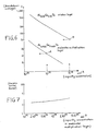
- Avalanche breakdown voltages of the n-type Al 0.28 Ga 0.72 Sb material used for the window layer 34 and of the n-type Al 0.065 Ga 0.935 Sb material used for the multiplication layer 33 are shown in Fig.6 depending on the impurity concentration.
- the pn junction formed in the window layer having a bigger band gap energy such as the n-type Al 0.28 Ga 0.72 Sb, can increase the avalanche breakdown voltage to a value higher than that formed by resonant impact ionization in an avalanche multiplication layer having a smaller band gap energy, such as the n-type Al 0.065 Ga 0.935 Sb, thus resulting in a lower tunnel current.
- both the resonant impact ionization taking place at a low voltage and the above-mentioned band gap energy difference contribute to prevent unexpected local avalanche breakdown.
- the avalanche breakdown voltage of the avalanche multiplication layer 33 is approximately 12 V, shown by the mark A, which is much less than the avalanche breakdown voltage of the window layer 34, which is approximately 50V as shown by the mark B.
- Fig.5 distributions of electric field intensity in the APD corresponding to the present invention is compared with that of the prior art APD. Because the avalanche multiplication layer 33 is located between the window layer 34 and the light absorbing layer 32, the electric field intensity applied to the light absorbing layer 32 having a small band gap energy becomes small; thus the dark current is reduced. Further, in Fig. 5, it is observed that the critical electric field intensity for the avalanche breakdown by resonant impact ionization, i.e. 4 x 10⁴ V/cm, is achieved at the avalanche multiplication layer 33, while the electric field intensity at the pn junction 36 in the window layer 34 is 1.2 x 10⁵ V/cm which is lower than its avalanche breakdown condition.
- the critical electric field intensity for the avalanche breakdown by resonant impact ionization i.e. 4 x 10⁴ V/cm
- the avalanche breakdown in the avalanche multiplication layer 33 is not affected by an undesirable local electric field at the pn junction, caused by an irregularity, such as a lattice defect or a sharp peripheral edge, in the window layer 34. Therefore, in the avalanche multiplication layer, the avalanche multiplication can always be initiated uniformly, not being affected by the electric field at the pn junction where the electric field is maximum. The multiplied great amount of positive holes becomes conductive carriers passing through the window layer 34 and the pn junction 36.
- the multiplication factor M easily reaches the value of 10 to 20 which is generally adopted and satisfactory in optical communication systems, and a value of 10 to 20 of the ionization rate ⁇ / ⁇ is easily achieved as well, resulting in a considerable reduction in the excessive noise factor and in an increase of the operation speed.
- Fig.7 shows the relation of the excessive noise factor F to the amount of the impurity concentration, when the n-type GaSb light-absorbing layer 32 receives light having a wave length of 1.55 micron, the positive holes produced therein being injected into the A1 0.065 Ga 0.935 Sb avalanche multiplication layer 33 and causing an avalanche multiplication whose multiplication factor is 10.
- the excessive noise factor F though varying with the value of the impurity concentration, remains approximately lower than 3. This value 3 is considerably lower than the value approximately equal to 5 achieved with the prior art APD using InP/GaInAs as shown in Fig.1.
- the high frequency response namely the cut off frequency
- the high frequency response is increased from approximately 3 GHZ, with the prior art APD of Fig.1, up to approximately 10 GHZ with the APD according to the present invention.
- the reduction of the field internally at the pn junction where the field intensity becomes maximum, the big band gap energy of the window layer and the reduction of the field intensity in the light absorbing layer contribute to achieve further reduction of the dark current.
- Another advantage of the invention lies in that the applied operating voltage is considerably reduced from approximately 100 V in the case of prior art APD of Fig.1, or from approximately 20 V in the case of the prior art APD of Fig.2, down to approximately 12.5 V.
- the fabrication of the APD of Fig.3 does not raise any difficult problems.
Landscapes
- Light Receiving Elements (AREA)
Applications Claiming Priority (2)
| Application Number | Priority Date | Filing Date | Title |
|---|---|---|---|
| JP86299/86 | 1986-04-15 | ||
| JP61086299A JPS62259481A (ja) | 1986-04-15 | 1986-04-15 | 半導体受光装置 |
Publications (2)
| Publication Number | Publication Date |
|---|---|
| EP0242298A2 true EP0242298A2 (de) | 1987-10-21 |
| EP0242298A3 EP0242298A3 (de) | 1989-05-24 |
Family
ID=13882953
Family Applications (1)
| Application Number | Title | Priority Date | Filing Date |
|---|---|---|---|
| EP87400859A Ceased EP0242298A3 (de) | 1986-04-15 | 1987-04-15 | Lawinen Fotodiode |
Country Status (4)
| Country | Link |
|---|---|
| US (1) | US4935795A (de) |
| EP (1) | EP0242298A3 (de) |
| JP (1) | JPS62259481A (de) |
| KR (1) | KR900005565B1 (de) |
Cited By (2)
| Publication number | Priority date | Publication date | Assignee | Title |
|---|---|---|---|---|
| EP0343970A3 (en) * | 1988-05-24 | 1990-05-23 | Nec Corporation | Planar type heterojunction avalanche photodiode |
| EP0325532A3 (en) * | 1988-01-18 | 1990-05-23 | Fujitsu Limited | A semiconductor photo-diode |
Families Citing this family (10)
| Publication number | Priority date | Publication date | Assignee | Title |
|---|---|---|---|---|
| JPH02159775A (ja) * | 1988-12-14 | 1990-06-19 | Toshiba Corp | 半導体受光素子及びその製造方法 |
| JP4956944B2 (ja) * | 2005-09-12 | 2012-06-20 | 三菱電機株式会社 | アバランシェフォトダイオード |
| US8269222B2 (en) | 2010-05-25 | 2012-09-18 | The United States Of America As Represented By The Secretary Of The Army | Semiconductor photodetector with transparent interface charge control layer and method thereof |
| US8269223B2 (en) | 2010-05-27 | 2012-09-18 | The United States Of America As Represented By The Secretary Of The Army | Polarization enhanced avalanche photodetector and method thereof |
| US9893227B2 (en) | 2013-05-24 | 2018-02-13 | The United States Of America As Represented By The Secretary Of The Army | Enhanced deep ultraviolet photodetector and method thereof |
| US9379271B2 (en) | 2013-05-24 | 2016-06-28 | The United States Of America As Represented By The Secretary Of The Army | Variable range photodetector and method thereof |
| JP6332096B2 (ja) * | 2015-03-23 | 2018-05-30 | 三菱電機株式会社 | 半導体受光素子 |
| US10381502B2 (en) * | 2015-09-09 | 2019-08-13 | Teledyne Scientific & Imaging, Llc | Multicolor imaging device using avalanche photodiode |
| US10032950B2 (en) * | 2016-02-22 | 2018-07-24 | University Of Virginia Patent Foundation | AllnAsSb avalanche photodiode and related method thereof |
| CN110061076B (zh) * | 2018-12-25 | 2024-05-24 | 芯思杰技术(深圳)股份有限公司 | 背入射式共面电极多单元芯片及其制备方法 |
Family Cites Families (11)
| Publication number | Priority date | Publication date | Assignee | Title |
|---|---|---|---|---|
| US3889284A (en) * | 1974-01-15 | 1975-06-10 | Us Army | Avalanche photodiode with varying bandgap |
| JPS5421294A (en) * | 1977-07-19 | 1979-02-17 | Mitsubishi Electric Corp | Avalanche photo diode |
| US4258375A (en) * | 1979-04-09 | 1981-03-24 | Massachusetts Institute Of Technology | Gax In1-x Asy P1-y /InP Avalanche photodiode and method for its fabrication |
| JPS5793585A (en) * | 1980-12-02 | 1982-06-10 | Fujitsu Ltd | Semiconductor photoreceiving element |
| JPS57198667A (en) * | 1981-06-01 | 1982-12-06 | Fujitsu Ltd | Light receiving element |
| US4403397A (en) * | 1981-07-13 | 1983-09-13 | The United States Of America As Represented By The Secretary Of The Navy | Method of making avalanche photodiodes |
| JPS592378A (ja) * | 1982-06-28 | 1984-01-07 | Fujitsu Ltd | アバランシェフォトダイオード |
| JPS6016474A (ja) * | 1983-07-08 | 1985-01-28 | Nec Corp | ヘテロ多重接合型光検出器 |
| JPS60105281A (ja) * | 1983-11-11 | 1985-06-10 | Fujitsu Ltd | 半導体受光装置 |
| US4651187A (en) * | 1984-03-22 | 1987-03-17 | Nec Corporation | Avalanche photodiode |
| JPS611064A (ja) * | 1984-05-31 | 1986-01-07 | Fujitsu Ltd | 半導体受光装置 |
-
1986
- 1986-04-15 JP JP61086299A patent/JPS62259481A/ja active Pending
-
1987
- 1987-04-14 KR KR1019870003576A patent/KR900005565B1/ko not_active Expired
- 1987-04-15 EP EP87400859A patent/EP0242298A3/de not_active Ceased
-
1989
- 1989-08-07 US US07/391,649 patent/US4935795A/en not_active Expired - Fee Related
Cited By (3)
| Publication number | Priority date | Publication date | Assignee | Title |
|---|---|---|---|---|
| EP0325532A3 (en) * | 1988-01-18 | 1990-05-23 | Fujitsu Limited | A semiconductor photo-diode |
| US4984032A (en) * | 1988-01-18 | 1991-01-08 | Fujitsu Limited | Semiconductor photodiode |
| EP0343970A3 (en) * | 1988-05-24 | 1990-05-23 | Nec Corporation | Planar type heterojunction avalanche photodiode |
Also Published As
| Publication number | Publication date |
|---|---|
| JPS62259481A (ja) | 1987-11-11 |
| KR900005565B1 (ko) | 1990-07-31 |
| KR870010640A (ko) | 1987-11-30 |
| EP0242298A3 (de) | 1989-05-24 |
| US4935795A (en) | 1990-06-19 |
Similar Documents
| Publication | Publication Date | Title |
|---|---|---|
| EP0800219B1 (de) | Heteroübergang-PIN-Photodiode | |
| US4442444A (en) | Avalanche photodiodes | |
| US4651187A (en) | Avalanche photodiode | |
| KR940011103B1 (ko) | 반도체 수광소자 | |
| EP0163546B1 (de) | Herstellungsverfahren einer Lawinenphotodiode und so hergestellte Lawinenphotodiode | |
| US4142200A (en) | Semiconductor photodiodes | |
| EP0142316A2 (de) | P-i-n- und Avalanche-Photodioden | |
| US20100133637A1 (en) | Avalanche photodiode | |
| US4390889A (en) | Photodiode having an InGaAs layer with an adjacent InGaAsP p-n junction | |
| EP0242298A2 (de) | Lawinen Fotodiode | |
| KR910009357B1 (ko) | 반도체 포토-다이오드 | |
| JP2708409B2 (ja) | 半導体受光素子およびその製造方法 | |
| US4471370A (en) | Majority carrier photodetector | |
| JPH05160426A (ja) | 半導体受光素子 | |
| US4346394A (en) | Gallium arsenide burrus FET structure for optical detection | |
| US3955082A (en) | Photodiode detector with selective frequency response | |
| KR950004550B1 (ko) | 수광소자 | |
| CA1228663A (en) | Photodetector with isolated avalanche region | |
| US4587544A (en) | Avalanche photodetector | |
| US5343054A (en) | Semiconductor light-detection device with recombination rates | |
| US4561007A (en) | Double mesa avalanche photodetector | |
| JPH038117B2 (de) | ||
| US4416053A (en) | Method of fabricating gallium arsenide burris FET structure for optical detection | |
| US4816890A (en) | Optoelectronic device | |
| EP0109855B1 (de) | Fotodiode mit einem Hetero-Übergang |
Legal Events
| Date | Code | Title | Description |
|---|---|---|---|
| PUAI | Public reference made under article 153(3) epc to a published international application that has entered the european phase |
Free format text: ORIGINAL CODE: 0009012 |
|
| AK | Designated contracting states |
Kind code of ref document: A2 Designated state(s): DE FR GB |
|
| PUAL | Search report despatched |
Free format text: ORIGINAL CODE: 0009013 |
|
| AK | Designated contracting states |
Kind code of ref document: A3 Designated state(s): DE FR GB |
|
| 17P | Request for examination filed |
Effective date: 19891113 |
|
| 17Q | First examination report despatched |
Effective date: 19910123 |
|
| STAA | Information on the status of an ep patent application or granted ep patent |
Free format text: STATUS: THE APPLICATION HAS BEEN REFUSED |
|
| 18R | Application refused |
Effective date: 19920807 |
|
| RIN1 | Information on inventor provided before grant (corrected) |
Inventor name: KANEDA, TAKAO Inventor name: MIKAWA, TAKASHI |