EP0242626A2 - Procédé pour le montage de composants électroniques sur un substrat - Google Patents
Procédé pour le montage de composants électroniques sur un substrat Download PDFInfo
- Publication number
- EP0242626A2 EP0242626A2 EP87104440A EP87104440A EP0242626A2 EP 0242626 A2 EP0242626 A2 EP 0242626A2 EP 87104440 A EP87104440 A EP 87104440A EP 87104440 A EP87104440 A EP 87104440A EP 0242626 A2 EP0242626 A2 EP 0242626A2
- Authority
- EP
- European Patent Office
- Prior art keywords
- sintering
- pressure
- substrate
- component
- temperature
- Prior art date
- Legal status (The legal status is an assumption and is not a legal conclusion. Google has not performed a legal analysis and makes no representation as to the accuracy of the status listed.)
- Granted
Links
Images

Classifications
-
- H—ELECTRICITY
- H10—SEMICONDUCTOR DEVICES; ELECTRIC SOLID-STATE DEVICES NOT OTHERWISE PROVIDED FOR
- H10W—GENERIC PACKAGES, INTERCONNECTIONS, CONNECTORS OR OTHER CONSTRUCTIONAL DETAILS OF DEVICES COVERED BY CLASS H10
- H10W20/00—Interconnections in chips, wafers or substrates
- H10W20/40—Interconnections external to wafers or substrates, e.g. back-end-of-line [BEOL] metallisations or vias connecting to gate electrodes
-
- H—ELECTRICITY
- H10—SEMICONDUCTOR DEVICES; ELECTRIC SOLID-STATE DEVICES NOT OTHERWISE PROVIDED FOR
- H10W—GENERIC PACKAGES, INTERCONNECTIONS, CONNECTORS OR OTHER CONSTRUCTIONAL DETAILS OF DEVICES COVERED BY CLASS H10
- H10W72/00—Interconnections or connectors in packages
- H10W72/30—Die-attach connectors
-
- H—ELECTRICITY
- H10—SEMICONDUCTOR DEVICES; ELECTRIC SOLID-STATE DEVICES NOT OTHERWISE PROVIDED FOR
- H10W—GENERIC PACKAGES, INTERCONNECTIONS, CONNECTORS OR OTHER CONSTRUCTIONAL DETAILS OF DEVICES COVERED BY CLASS H10
- H10W72/00—Interconnections or connectors in packages
- H10W72/01—Manufacture or treatment
- H10W72/013—Manufacture or treatment of die-attach connectors
- H10W72/01365—Thermally treating
-
- H—ELECTRICITY
- H10—SEMICONDUCTOR DEVICES; ELECTRIC SOLID-STATE DEVICES NOT OTHERWISE PROVIDED FOR
- H10W—GENERIC PACKAGES, INTERCONNECTIONS, CONNECTORS OR OTHER CONSTRUCTIONAL DETAILS OF DEVICES COVERED BY CLASS H10
- H10W72/00—Interconnections or connectors in packages
- H10W72/071—Connecting or disconnecting
- H10W72/073—Connecting or disconnecting of die-attach connectors
-
- H—ELECTRICITY
- H10—SEMICONDUCTOR DEVICES; ELECTRIC SOLID-STATE DEVICES NOT OTHERWISE PROVIDED FOR
- H10W—GENERIC PACKAGES, INTERCONNECTIONS, CONNECTORS OR OTHER CONSTRUCTIONAL DETAILS OF DEVICES COVERED BY CLASS H10
- H10W72/00—Interconnections or connectors in packages
- H10W72/071—Connecting or disconnecting
- H10W72/073—Connecting or disconnecting of die-attach connectors
- H10W72/07311—Treating the bonding area before connecting, e.g. by applying flux or cleaning
-
- H—ELECTRICITY
- H10—SEMICONDUCTOR DEVICES; ELECTRIC SOLID-STATE DEVICES NOT OTHERWISE PROVIDED FOR
- H10W—GENERIC PACKAGES, INTERCONNECTIONS, CONNECTORS OR OTHER CONSTRUCTIONAL DETAILS OF DEVICES COVERED BY CLASS H10
- H10W72/00—Interconnections or connectors in packages
- H10W72/071—Connecting or disconnecting
- H10W72/073—Connecting or disconnecting of die-attach connectors
- H10W72/07331—Connecting techniques
-
- H—ELECTRICITY
- H10—SEMICONDUCTOR DEVICES; ELECTRIC SOLID-STATE DEVICES NOT OTHERWISE PROVIDED FOR
- H10W—GENERIC PACKAGES, INTERCONNECTIONS, CONNECTORS OR OTHER CONSTRUCTIONAL DETAILS OF DEVICES COVERED BY CLASS H10
- H10W72/00—Interconnections or connectors in packages
- H10W72/071—Connecting or disconnecting
- H10W72/073—Connecting or disconnecting of die-attach connectors
- H10W72/07331—Connecting techniques
- H10W72/07336—Soldering or alloying
-
- H—ELECTRICITY
- H10—SEMICONDUCTOR DEVICES; ELECTRIC SOLID-STATE DEVICES NOT OTHERWISE PROVIDED FOR
- H10W—GENERIC PACKAGES, INTERCONNECTIONS, CONNECTORS OR OTHER CONSTRUCTIONAL DETAILS OF DEVICES COVERED BY CLASS H10
- H10W72/00—Interconnections or connectors in packages
- H10W72/30—Die-attach connectors
- H10W72/321—Structures or relative sizes of die-attach connectors
- H10W72/325—Die-attach connectors having a filler embedded in a matrix
-
- H—ELECTRICITY
- H10—SEMICONDUCTOR DEVICES; ELECTRIC SOLID-STATE DEVICES NOT OTHERWISE PROVIDED FOR
- H10W—GENERIC PACKAGES, INTERCONNECTIONS, CONNECTORS OR OTHER CONSTRUCTIONAL DETAILS OF DEVICES COVERED BY CLASS H10
- H10W72/00—Interconnections or connectors in packages
- H10W72/30—Die-attach connectors
- H10W72/351—Materials of die-attach connectors
- H10W72/352—Materials of die-attach connectors comprising metals or metalloids, e.g. solders
-
- Y—GENERAL TAGGING OF NEW TECHNOLOGICAL DEVELOPMENTS; GENERAL TAGGING OF CROSS-SECTIONAL TECHNOLOGIES SPANNING OVER SEVERAL SECTIONS OF THE IPC; TECHNICAL SUBJECTS COVERED BY FORMER USPC CROSS-REFERENCE ART COLLECTIONS [XRACs] AND DIGESTS
- Y10—TECHNICAL SUBJECTS COVERED BY FORMER USPC
- Y10S—TECHNICAL SUBJECTS COVERED BY FORMER USPC CROSS-REFERENCE ART COLLECTIONS [XRACs] AND DIGESTS
- Y10S148/00—Metal treatment
- Y10S148/012—Bonding, e.g. electrostatic for strain gauges
-
- Y—GENERAL TAGGING OF NEW TECHNOLOGICAL DEVELOPMENTS; GENERAL TAGGING OF CROSS-SECTIONAL TECHNOLOGIES SPANNING OVER SEVERAL SECTIONS OF THE IPC; TECHNICAL SUBJECTS COVERED BY FORMER USPC CROSS-REFERENCE ART COLLECTIONS [XRACs] AND DIGESTS
- Y10—TECHNICAL SUBJECTS COVERED BY FORMER USPC
- Y10S—TECHNICAL SUBJECTS COVERED BY FORMER USPC CROSS-REFERENCE ART COLLECTIONS [XRACs] AND DIGESTS
- Y10S148/00—Metal treatment
- Y10S148/054—Flat sheets-substrates
Definitions
- the invention relates to a method for fastening electronic components, in particular large-area power semiconductors, to a substrate by pressure sintering.
- a substrate made of molybdenum, a plate made of aluminum and a semiconductor body made of silicon are first connected to one another by heating to about 700-800 ° C., the connection between aluminum and molybdenum being one type Solder connection can be viewed while the connection between aluminum and silicon is effected by the formation of a eutectic alloy. During this alloying process, silicon is doped at the same time. Due to the different thermal expansion coefficients of the individual parts, the high temperature load leads to high stresses in the power semiconductor, which is noticeable in the finished product through corresponding warping.
- MOS technology accuracies in the range of ⁇ m are made possible in the case of doping and in the production of structures by using photoresist techniques and etching techniques.
- application of MOS technology to the production of large-area power semiconductors has not hitherto been possible, since the high temperatures required for alloying onto a substrate have increased would destroy the pn junctions and the fine aluminum structures. It would also not be possible to produce the structures after the silicon had been alloyed onto the substrate, since the existing warpage would preclude the use of photoresist techniques and etching techniques with accuracies in the range of ⁇ m.
- connection layers produced by pressure sintering were always inhomogeneous and interspersed with channel-like structures, which accordingly led to low adhesive strengths, high electrical contact resistance and high thermal resistance.
- the invention has for its object to provide a method for mounting electronic components on a substrate by pressure sintering, which is also suitable for large-area power semiconductors.
- electronic components produced by MOS technology should also be able to be attached to a substrate with low thermal stress.
- the invention is based on the knowledge that the paste consisting of metal powder and a solvent must be dried before the component is placed on the substrate, since otherwise the solvent vapor lifts large components and escapes to the outside via a system of channels formed in the paste.
- the previous drying of the paste leads to relatively rough surfaces in the contact area, although this disadvantage can be compensated for by increasing the mechanical pressure during pressure sintering to at least 900 N / cm2.
- the powder of a noble metal or a noble metal alloy is used as the metal powder.
- the connecting layers then have particularly low electrical contact resistances. It has proven to be particularly favorable if silver powder or the powder of a silver alloy is used as the metal powder.
- a mechanical pressure of at least 1000 N / cm2 is exerted during pressure sintering.
- a further increase in the quality of the connection is achieved if a mechanical pressure of at least 1500 N / cm2 is exerted during pressure sintering. It has proven to be advantageous if a mechanical pressure is exerted during pressure sintering which corresponds at least to the intended operating pressure of a pressure-contacted component.
- pressure sintering can be carried out at a sintering temperature of at least 150 ° C. Even better connections are achieved, however, if the pressure sintering is carried out at a sintering temperature between 180 ° C and 250 ° C. Sintering temperature of 250 ° C and less are particularly favorable, in particular, if the components for irradiation adjustment are irradiated with electrons or protons, since higher temperatures would counteract the effect of this irradiation.
- the pressure sintering is carried out in a press with heated punches.
- the heating to the sintering temperature with simultaneous application of the required mechanical pressure is then particularly simple, and the suitability for mass production should also be emphasized.
- the upper side of the component can then be protected by a deformable intermediate layer during pressure sintering.
- a second intermediate layer made of a hard material with low thermal expansion can then also be arranged during the pressure sintering over the intermediate layer. This second rigid intermediate layer then ensures that thermal expansions of the press ram are not transferred to the component or its fine structures.
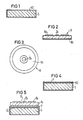
- the substrate S is, for example, a 1.5 mm thick disk made of molybdenum with a diameter of 29.6 mm.
- the electroplated contact surface KO is about 2 to 3 ⁇ m thick and consists of silver.
- This component B is a large-area thyristor, on the upper side of which an ignition contact Zk and a cathode Ka can be seen as aluminum structures.
- a paste P is applied in layer form to the contact surface KO of the substrate S.
- Paste P is applied in a layer thickness of between 10 and 100 ⁇ m, preferably of approximately 20 ⁇ m, by screen printing.
- Silver powder with platelet-shaped powder particles, a grain size ⁇ 15 ⁇ m and a bulk density of approx. 1.9 g / ml is used as the starting material for the production of paste P.
- This silver powder is then suspended in cyclohexanol as a solvent in a weight ratio of about 2: 1.
- the paste P which can be screen-printed in this way is then degassed in vacuo in order to prevent void formation later during drying or sintering.
- the substrate S and the component B are heated together or separately to a temperature which is at least 100 ° C. but is still below the sintering temperature.
- This pressureless heating can also be carried out in a press to be explained later.
- the component B according to FIG. 5 with its contacting layer KS is placed on the completely dried paste P of the substrate S.
- the entire arrangement is then introduced into a press, of which the upper punch St1 and the lower stamp St2 can be seen.
- an approximately 80 ⁇ m thick first intermediate layer Z1 made of aluminum and a very stiff approximately 1.5 mm thick intermediate layer Z2 made of molybdenum are arranged in succession, the arrangement of these parts in Fig 6 is shown in an exploded state for better identification.
- the two stamps St1 and St2 of the press are heated so that the desired sintering temperature is reached in the structure arranged between them.
- This sintering temperature which is, for example, 230 ° C., is then maintained for about 1 minute, a mechanical pressure of 1500 N / cm 2 being simultaneously exerted on the entire arrangement via the punches St1 and St2.
- the mechanical pressure can possibly also be increased to 1-2 tons per cm2.
- the pressure sintering is carried out in a normal atmosphere, i. H. it is not necessary to use protective gas or forming gas.
- This pressure-free re-sintering which could also be referred to as tempering, is carried out, for example, at a temperature of approximately 250 ° C., a period of just 5 minutes leading to a considerable improvement in the mechanical strength.
- connection of the semiconductor body and substrate is carried out by pressure sintering, the Sintering should always proceed as a solid-state reaction without the occurrence of liquid phases.
- the method described is particularly suitable for large-area power semiconductors manufactured using MOS technology, although considerable advantages can also be achieved in the manufacture of other electronic components.
Landscapes
- Electrodes Of Semiconductors (AREA)
- Die Bonding (AREA)
Applications Claiming Priority (2)
| Application Number | Priority Date | Filing Date | Title |
|---|---|---|---|
| DE3613572 | 1986-04-22 | ||
| DE3613572 | 1986-04-22 |
Publications (3)
| Publication Number | Publication Date |
|---|---|
| EP0242626A2 true EP0242626A2 (fr) | 1987-10-28 |
| EP0242626A3 EP0242626A3 (en) | 1989-01-25 |
| EP0242626B1 EP0242626B1 (fr) | 1991-06-12 |
Family
ID=6299247
Family Applications (1)
| Application Number | Title | Priority Date | Filing Date |
|---|---|---|---|
| EP19870104440 Expired - Lifetime EP0242626B1 (fr) | 1986-04-22 | 1987-03-25 | Procédé pour le montage de composants électroniques sur un substrat |
Country Status (6)
| Country | Link |
|---|---|
| US (1) | US4810672A (fr) |
| EP (1) | EP0242626B1 (fr) |
| JP (1) | JP2515708B2 (fr) |
| BR (1) | BR8701876A (fr) |
| DE (1) | DE3770683D1 (fr) |
| IN (1) | IN168174B (fr) |
Cited By (26)
| Publication number | Priority date | Publication date | Assignee | Title |
|---|---|---|---|---|
| EP0715351A1 (fr) | 1994-12-02 | 1996-06-05 | eupec Europäische Gesellschaft für Leistungshalbleiter mbH & Co. KG | Composant semi-conducteur de puissance |
| WO1998013863A1 (fr) * | 1996-09-27 | 1998-04-02 | Siemens Aktiengesellschaft | Procede de metallisation d'une puce a bosses de semi-conducteur, possedant peu de connexions |
| EP0764978A3 (fr) * | 1995-09-11 | 1999-04-21 | Siemens Aktiengesellschaft | Procédé pour la fixation de composants électroniques au dessus d'un substrat au moyen de frittage par pression |
| EP0824270A3 (fr) * | 1996-08-06 | 1999-06-09 | Hitachi Chemical Co., Ltd. | Procédé pour le montage d'une pluralité de pièces électroniques sur un panneau de circuit |
| DE10009678C1 (de) * | 2000-02-29 | 2001-07-19 | Siemens Ag | Wärmeleitende Klebstoffverbindung und Verfahren zum Herstellen einer wärmeleitenden Klebstoffverbindung |
| DE10016129A1 (de) * | 2000-03-31 | 2001-10-18 | Siemens Ag | Verfahren zum Herstellen einer wärmeleitenden Verbindung zwischen zwei Werkstücken |
| WO2004010752A1 (fr) * | 2002-07-23 | 2004-01-29 | Elmicron Ag | Procede de fixation d'elements de micro-outils sur des objets |
| US6812559B2 (en) | 2000-12-13 | 2004-11-02 | Daimlerchrysler Ag | Power module with improved transient thermal impedance |
| FR2915622A1 (fr) * | 2007-04-30 | 2008-10-31 | Valeo Electronique Sys Liaison | Procde d'assemblage d'un organe sur un support par frittage d'une masse de poudre conductrice |
| DE102007022336A1 (de) * | 2007-05-12 | 2008-11-20 | Semikron Elektronik Gmbh & Co. Kg | Leistungshalbleitersubstrat mit Metallkontaktschicht sowie Herstellungsverfahren hierzu |
| EP2075835A2 (fr) | 2007-12-28 | 2009-07-01 | Robert Bosch Gmbh | Diode avec moyens pour la réduction de contraintes mécaniques |
| US7682875B2 (en) | 2008-05-28 | 2010-03-23 | Infineon Technologies Ag | Method for fabricating a module including a sintered joint |
| WO2010072555A1 (fr) * | 2008-12-23 | 2010-07-01 | Robert Bosch Gmbh | Composant électrique ou électronique composite et procédé de fabrication d'un composant électrique ou électronique composite |
| WO2010072667A1 (fr) * | 2008-12-23 | 2010-07-01 | Robert Bosch Gmbh | Élément composite électrique ou électronique et procédé de fabrication d'un élément composite électrique ou électronique |
| WO2010091660A3 (fr) * | 2009-02-13 | 2011-06-03 | Danfoss Silicon Power Gmbh | Procédé pour créer une liaison résistant aux températures élevées et aux changements de température d'un semi-conducteur de module et d'un composant semi-conducteur avec un procédé agissant sur la température |
| EP2390914A1 (fr) * | 2010-05-27 | 2011-11-30 | SEMIKRON Elektronik GmbH & Co. KG | Agencement de deux partenaires de liaison à l'aide d'une interconnexion de pression à basse température et son procédé de fabrication |
| US8253233B2 (en) | 2008-02-14 | 2012-08-28 | Infineon Technologies Ag | Module including a sintered joint bonding a semiconductor chip to a copper surface |
| WO2012079855A3 (fr) * | 2010-12-14 | 2012-09-20 | Robert Bosch Gmbh | Ensemble électronique doté d'une liaison par frittage améliorée |
| US8587116B2 (en) | 2010-09-30 | 2013-11-19 | Infineon Technologies Ag | Semiconductor module comprising an insert |
| WO2013185839A1 (fr) * | 2012-06-15 | 2013-12-19 | Osram Opto Semiconductors Gmbh | Procédé de fabrication d'un composant à semi-conducteur optoélectronique comprenant une couche de liaison frittée sous l'action de la chaleur, d'une pression et d'ultrasons |
| EP2390904A3 (fr) * | 2010-05-27 | 2014-03-26 | SEMIKRON Elektronik GmbH & Co. KG | Procédé d'interconnexion de pression à basse température de deux partenaires de liaison et agencement ainsi fabriqué |
| DE102014105000A1 (de) * | 2014-04-08 | 2015-10-08 | Infineon Technologies Ag | Verfahren zur Herstellung und zum Bestücken eines Schaltungsträgers |
| US9214442B2 (en) | 2007-03-19 | 2015-12-15 | Infineon Technologies Ag | Power semiconductor module, method for producing a power semiconductor module, and semiconductor chip |
| DE102015114314A1 (de) * | 2015-08-28 | 2017-03-02 | Innovative Sensor Technology Ist Ag | Verfahren zur Herstellung eines Temperatursensors |
| WO2019219322A1 (fr) * | 2018-05-18 | 2019-11-21 | Endress+Hauser Wetzer Gmbh+Co. Kg | Procédé pour la fabrication d'un thermomètre |
| WO2021259536A2 (fr) | 2020-06-23 | 2021-12-30 | Siemens Aktiengesellschaft | Procédé de mise en contact d'un semi-conducteur de puissance sur un substrat |
Families Citing this family (56)
| Publication number | Priority date | Publication date | Assignee | Title |
|---|---|---|---|---|
| DE3777995D1 (de) * | 1986-12-22 | 1992-05-07 | Siemens Ag | Verfahren zur befestigung von elektronischen bauelementen auf einem substrat, folie zur durchfuehrung des verfahrens und verfahren zur herstellung der folie. |
| EP0330895B1 (fr) * | 1988-03-03 | 1994-12-14 | Siemens Aktiengesellschaft | Procédé pour fixer des composants électroniques sur des substrats et dispositif pour sa réalisation |
| EP0330896A3 (fr) * | 1988-03-03 | 1991-01-09 | Siemens Aktiengesellschaft | Procédé pour fixer des composants semi-conducteurs sur des substrats et dispositifs pour sa réalisation |
| US4927069A (en) * | 1988-07-15 | 1990-05-22 | Sanken Electric Co., Ltd. | Soldering method capable of providing a joint of reduced thermal resistance |
| DE3917765C2 (de) * | 1989-05-31 | 1996-05-30 | Siemens Ag | Verfahren zum Verbinden von zwei scheibenförmigen Körpern aus Materialien unterschiedlicher thermischer Ausdehnungskoeffizienten und dessen Verwendung |
| US5118029A (en) * | 1989-11-30 | 1992-06-02 | The Furukawa Electric Co., Ltd. | Method of forming a solder layer on pads of a circuit board and method of mounting an electronic part on a circuit board |
| EP0460286A3 (en) * | 1990-06-06 | 1992-02-26 | Siemens Aktiengesellschaft | Method and arrangement for bonding a semiconductor component to a substrate or for finishing a semiconductor/substrate connection by contactless pressing |
| EP0477600A1 (fr) * | 1990-09-26 | 1992-04-01 | Siemens Aktiengesellschaft | Procédé pour attacher à un substrat un corps semi-conducteur comportant au moins un composant semi-conducteur |
| US5693574A (en) * | 1991-02-22 | 1997-12-02 | Deutsche Aerospace Ag | Process for the laminar joining of silicon semiconductor slices |
| DE4110318C2 (de) * | 1991-03-28 | 2001-10-11 | Bosch Gmbh Robert | Verfahren zum Zusammenlöten zweier Bauteile |
| DE59209470D1 (de) * | 1991-06-24 | 1998-10-01 | Siemens Ag | Halbleiterbauelement und Verfahren zu seiner Herstellung |
| US5403783A (en) * | 1992-12-28 | 1995-04-04 | Hitachi, Ltd. | Integrated circuit substrate with cooling accelerator substrate |
| DE4315272A1 (de) * | 1993-05-07 | 1994-11-10 | Siemens Ag | Leistungshalbleiterbauelement mit Pufferschicht |
| US5607882A (en) * | 1994-12-20 | 1997-03-04 | Lucent Technologies Inc. | Multi-component electronic devices and methods for making them |
| US5967030A (en) | 1995-11-17 | 1999-10-19 | Micron Technology, Inc. | Global planarization method and apparatus |
| US6316363B1 (en) | 1999-09-02 | 2001-11-13 | Micron Technology, Inc. | Deadhesion method and mechanism for wafer processing |
| US6331488B1 (en) * | 1997-05-23 | 2001-12-18 | Micron Technology, Inc. | Planarization process for semiconductor substrates |
| US6218316B1 (en) | 1998-10-22 | 2001-04-17 | Micron Technology, Inc. | Planarization of non-planar surfaces in device fabrication |
| CN1191144C (zh) * | 2000-05-08 | 2005-03-02 | 布莱阿姆青年大学 | 摩擦搅拌焊接的超级研磨工具和方法 |
| US6518172B1 (en) | 2000-08-29 | 2003-02-11 | Micron Technology, Inc. | Method for applying uniform pressurized film across wafer |
| DE10140826B4 (de) * | 2000-12-13 | 2005-11-10 | Infineon Technologies Ag | Verfahren zur mehrschrittigen Bearbeitung eines dünnen und unter den Bearbeitungsschritten bruchgefährdeten Halbleiter-Waferprodukts |
| DE10334391B4 (de) * | 2003-07-28 | 2005-10-06 | Fraunhofer-Gesellschaft zur Förderung der angewandten Forschung e.V. | Verfahren zur Erzeugung von Verbindungen in der Mikroelektronik |
| US20050098613A1 (en) * | 2003-11-07 | 2005-05-12 | Barker William W. | Method for diffusion bond welding for use in a multilayer electronic assembly |
| US8257795B2 (en) * | 2004-02-18 | 2012-09-04 | Virginia Tech Intellectual Properties, Inc. | Nanoscale metal paste for interconnect and method of use |
| DE102004019567B3 (de) * | 2004-04-22 | 2006-01-12 | Semikron Elektronik Gmbh & Co. Kg | Verfahren zur Befestigung von elektronischen Bauelementen auf einem Substrat |
| DE102004056702B3 (de) * | 2004-04-22 | 2006-03-02 | Semikron Elektronik Gmbh & Co. Kg | Verfahren zur Befestigung von elektronischen Bauelementen auf einem Substrat |
| EP1783829A1 (fr) | 2005-11-02 | 2007-05-09 | Abb Research Ltd. | Procédé pour la fixation de composants électroniques |
| DE102005058794A1 (de) * | 2005-12-09 | 2007-06-14 | Semikron Elektronik Gmbh & Co. Kg | Vorrichtung und getaktetes Verfahren zur Drucksinterverbindung |
| DE102006014145C5 (de) * | 2006-03-28 | 2015-12-17 | Semikron Elektronik Gmbh & Co. Kg | Druck kontaktierte Anordnung mit einem Leistungsbauelement, einem Metallformkörper und einer Verbindungseinrichtung |
| DE102006031844B4 (de) * | 2006-07-07 | 2013-04-11 | Technische Universität Braunschweig Carolo-Wilhelmina | Verfahren zur Befestigung von elektronischen Bauelementen auf einem Träger durch Drucksinterung und somit hergestellte Schaltungsanordnung |
| DE102006033073B3 (de) * | 2006-07-14 | 2008-02-14 | Danfoss Silicon Power Gmbh | Verfahren zur Schaffung einer hitze- und stoßfesten Verbindung des Baugruppen-Halbleiters und zur Drucksinterung vorbereiteter Halbleiterbaustein |
| DE102007022337A1 (de) * | 2007-05-12 | 2008-11-20 | Semikron Elektronik Gmbh & Co. Kg | Gesintertes Leistungshalbleitersubstrat sowie Herstellungsverfahren hierzu |
| DE102007035324A1 (de) * | 2007-07-27 | 2009-01-29 | Robert Bosch Gmbh | Verfahren zum Befestigen von mindestens einem elektronischen Bauelement an einem Stator einer elektrischen Maschine |
| DE102008048869A1 (de) * | 2008-09-25 | 2010-04-22 | Infineon Technologies Ag | Vorrichtung und Verfahren zum Verbinden zweier Verbindungspartner |
| DE102009017692B4 (de) | 2009-04-09 | 2020-08-27 | Fraunhofer-Gesellschaft zur Förderung der angewandten Forschung e.V. | Verfahren zur Herstellung einer Niedertemperaturkontaktierung für mikroelektronische Aufbauten |
| DE102009020733B4 (de) * | 2009-05-11 | 2011-12-08 | Danfoss Silicon Power Gmbh | Verfahren zur Kontaktsinterung von bandförmigen Kontaktelementen |
| DE102010001666A1 (de) | 2010-02-08 | 2011-08-11 | Robert Bosch GmbH, 70469 | Elektrisches oder elektronisches Verbundbauteil |
| DE102010044329A1 (de) | 2010-09-03 | 2012-03-08 | Heraeus Materials Technology Gmbh & Co. Kg | Kontaktierungsmittel und Verfahren zur Kontaktierung elektrischer Bauteile |
| WO2012061511A2 (fr) | 2010-11-03 | 2012-05-10 | Fry's Metals, Inc. | Matériaux de frittage et procédés de fixation les utilisant |
| US8999758B2 (en) | 2011-08-12 | 2015-04-07 | Infineon Technologies Ag | Fixing semiconductor die in dry and pressure supported assembly processes |
| EP2560468A1 (fr) | 2011-08-19 | 2013-02-20 | ABB Research Ltd. | Procédé de connexion d'éléments provenant de plusieurs éléments à un autre |
| DE102011083926A1 (de) | 2011-09-30 | 2013-04-04 | Robert Bosch Gmbh | Schichtverbund aus einer Trägerfolie und einer Schichtanordnung umfassend eine sinterbare Schicht aus mindestens einem Metallpulver und eine Lotschicht |
| DE102012107570B4 (de) * | 2012-08-17 | 2017-08-03 | Rogers Germany Gmbh | Verfahren zur Herstellung von Hohlkörpern, insbesondere von Kühlern, Hohlkörper sowie Kühler enthaltende elektrische oder elektronische Baugruppen |
| DE102013101124B4 (de) | 2013-02-05 | 2020-12-03 | Seho Systemtechnik Gmbh | Vorrichtung und Verfahren zum Sintern eines Sinterproduktes |
| DE102014103013B4 (de) * | 2014-03-06 | 2017-09-21 | Infineon Technologies Ag | Verfahren zum Erzeugen einer getrockneten Pastenschicht, Verfahren zum Erzeugen einer Sinterverbindung und Durchlaufanlage zur Durchführung der Verfahren |
| RU2564518C1 (ru) * | 2014-07-01 | 2015-10-10 | Федеральное государственное унитарное предприятие "Всероссийский научно-исследовательский институт авиационных материалов" (ФГУП "ВИАМ") | Способ сушки покрытия из серебросодержащей пасты |
| EP3208841B1 (fr) * | 2016-02-19 | 2020-12-09 | Heraeus Deutschland GmbH & Co. KG | Procede de fabrication d'une plaque de dissipation thermique, plaque de dissipation thermique, procede de fabrication d'un module a semi-conducteurs et module a semi-conducteurs |
| DE102016108000B3 (de) * | 2016-04-29 | 2016-12-15 | Danfoss Silicon Power Gmbh | Verfahren zum stoffschlüssigen Verbinden einer ersten Komponente eines Leistungshalbleitermoduls mit einer zweiten Komponente eines Leistungshalbleitermoduls |
| DE102018133090A1 (de) * | 2018-12-20 | 2020-06-25 | Danfoss Silicon Power Gmbh | Anordnung zum Sintern einer elektronischen Baugruppe |
| FR3095142B1 (fr) | 2019-04-18 | 2023-08-25 | Isp System | Procédé et dispositif de fabrication de préformes destinées à la brasure de composants électroniques, photoniques, thermiques ou mécaniques. |
| EP3792962A1 (fr) | 2019-09-12 | 2021-03-17 | Infineon Technologies AG | Méthode de contrôle d'un procédé de fabrication d'une couche frittable de connexion par mesures photométriques |
| DE102019134595A1 (de) * | 2019-12-16 | 2021-06-17 | Endress+Hauser SE+Co. KG | Fügen von zwei Bauteilen eines Feldgeräts der Prozess- und Automatisierungstechnik |
| US12048971B2 (en) | 2020-12-04 | 2024-07-30 | Isp System | Manufacturing process and device for preforms intended for brazing electronic, photonic, thermal or mechanical components |
| US20220230989A1 (en) * | 2021-01-18 | 2022-07-21 | Nitto Denko Corporation | Semiconductor device and method for producing semiconductor device |
| DE102022133386A1 (de) * | 2022-12-15 | 2024-06-20 | Pac Tech - Packaging Technologies Gmbh | Verfahren zur Herstellung einer Lötkontaktfläche auf einem Chip durch Erzeugung einer Sinterpastenschnittstelle |
| CN118527650A (zh) | 2023-02-23 | 2024-08-23 | 通用汽车环球科技运作有限责任公司 | 制备低温烧结银膏的方法 |
Family Cites Families (12)
| Publication number | Priority date | Publication date | Assignee | Title |
|---|---|---|---|---|
| US2390452A (en) * | 1942-11-26 | 1945-12-04 | Int Nickel Co | Method of producing composite metal stock |
| US3479731A (en) * | 1967-06-13 | 1969-11-25 | Gen Motors Corp | Brazing method |
| US3716347A (en) * | 1970-09-21 | 1973-02-13 | Minnesota Mining & Mfg | Metal parts joined with sintered powdered metal |
| GB2067117B (en) * | 1980-01-02 | 1983-07-06 | Secr Defence | Bonding semi-conductor bodies to aluminium thick-film circuits |
| JPS5731148A (en) * | 1980-07-31 | 1982-02-19 | Fujitsu Ltd | Manufacture of semiconductor device |
| JPS5811245U (ja) * | 1981-07-15 | 1983-01-25 | 日本電気株式会社 | 半導体装置 |
| JPS58112335A (ja) * | 1981-12-26 | 1983-07-04 | Nitto Electric Ind Co Ltd | 半導体素子固定用接着フイルム |
| SE430481B (sv) * | 1982-03-29 | 1983-11-21 | Asea Ab | Sett att sammanfoga delar av solitt material genom varm isostatisk pressning |
| JPS5952854A (ja) * | 1982-09-20 | 1984-03-27 | Hitachi Ltd | 絶縁型半導体装置の製法 |
| JPS59181628A (ja) * | 1983-03-31 | 1984-10-16 | Toshiba Corp | 半導体素子の固着方法 |
| US4574329A (en) * | 1983-10-07 | 1986-03-04 | U.S. Philips Corporation | Multilayer ceramic capacitor |
| DE3414065A1 (de) * | 1984-04-13 | 1985-12-12 | Siemens AG, 1000 Berlin und 8000 München | Anordnung bestehend aus mindestens einem auf einem substrat befestigten elektronischen bauelement und verfahren zur herstellung einer derartigen anordnung |
-
1987
- 1987-03-10 IN IN195/CAL/87A patent/IN168174B/en unknown
- 1987-03-25 DE DE8787104440T patent/DE3770683D1/de not_active Expired - Lifetime
- 1987-03-25 EP EP19870104440 patent/EP0242626B1/fr not_active Expired - Lifetime
- 1987-03-25 US US07/029,819 patent/US4810672A/en not_active Expired - Lifetime
- 1987-04-17 JP JP9611787A patent/JP2515708B2/ja not_active Expired - Lifetime
- 1987-04-21 BR BR8701876A patent/BR8701876A/pt unknown
Cited By (39)
| Publication number | Priority date | Publication date | Assignee | Title |
|---|---|---|---|---|
| EP0715351A1 (fr) | 1994-12-02 | 1996-06-05 | eupec Europäische Gesellschaft für Leistungshalbleiter mbH & Co. KG | Composant semi-conducteur de puissance |
| EP0764978A3 (fr) * | 1995-09-11 | 1999-04-21 | Siemens Aktiengesellschaft | Procédé pour la fixation de composants électroniques au dessus d'un substrat au moyen de frittage par pression |
| US6841022B2 (en) | 1996-08-06 | 2005-01-11 | Hitachi Chemical Company, Ltd. | Adhesive-coated electronic parts on a connection sheet |
| EP0824270A3 (fr) * | 1996-08-06 | 1999-06-09 | Hitachi Chemical Co., Ltd. | Procédé pour le montage d'une pluralité de pièces électroniques sur un panneau de circuit |
| WO1998013863A1 (fr) * | 1996-09-27 | 1998-04-02 | Siemens Aktiengesellschaft | Procede de metallisation d'une puce a bosses de semi-conducteur, possedant peu de connexions |
| WO2001065603A1 (fr) * | 2000-02-29 | 2001-09-07 | Siemens Aktiengesellschaft | Assemblage colle thermoconducteur, et procede de realisation d'un assemblage colle thermoconducteur |
| US6823915B2 (en) | 2000-02-29 | 2004-11-30 | Siemens Aktiengesellschaft | Heat-conducting adhesive joint with an adhesive-filled, porous heat conductor |
| DE10009678C1 (de) * | 2000-02-29 | 2001-07-19 | Siemens Ag | Wärmeleitende Klebstoffverbindung und Verfahren zum Herstellen einer wärmeleitenden Klebstoffverbindung |
| DE10016129A1 (de) * | 2000-03-31 | 2001-10-18 | Siemens Ag | Verfahren zum Herstellen einer wärmeleitenden Verbindung zwischen zwei Werkstücken |
| US6812559B2 (en) | 2000-12-13 | 2004-11-02 | Daimlerchrysler Ag | Power module with improved transient thermal impedance |
| WO2004010752A1 (fr) * | 2002-07-23 | 2004-01-29 | Elmicron Ag | Procede de fixation d'elements de micro-outils sur des objets |
| US9214442B2 (en) | 2007-03-19 | 2015-12-15 | Infineon Technologies Ag | Power semiconductor module, method for producing a power semiconductor module, and semiconductor chip |
| US8444913B2 (en) | 2007-04-30 | 2013-05-21 | Valeo Etudes Electroniques | Method of assembling a member on a support by sintering a mass of conductive powder |
| FR2915622A1 (fr) * | 2007-04-30 | 2008-10-31 | Valeo Electronique Sys Liaison | Procde d'assemblage d'un organe sur un support par frittage d'une masse de poudre conductrice |
| WO2008145930A3 (fr) * | 2007-04-30 | 2009-03-05 | Valeo Etudes Electroniques | Procede d'assemblage d'un organe sur un support par frittage d'une masse de poudre conductrice |
| DE102007022336A1 (de) * | 2007-05-12 | 2008-11-20 | Semikron Elektronik Gmbh & Co. Kg | Leistungshalbleitersubstrat mit Metallkontaktschicht sowie Herstellungsverfahren hierzu |
| DE102007063308A1 (de) | 2007-12-28 | 2009-07-02 | Robert Bosch Gmbh | Diode |
| EP2075835A2 (fr) | 2007-12-28 | 2009-07-01 | Robert Bosch Gmbh | Diode avec moyens pour la réduction de contraintes mécaniques |
| US8253233B2 (en) | 2008-02-14 | 2012-08-28 | Infineon Technologies Ag | Module including a sintered joint bonding a semiconductor chip to a copper surface |
| US8415207B2 (en) | 2008-02-14 | 2013-04-09 | Infineon Technologies Ag | Module including a sintered joint bonding a semiconductor chip to a copper surface |
| US7682875B2 (en) | 2008-05-28 | 2010-03-23 | Infineon Technologies Ag | Method for fabricating a module including a sintered joint |
| WO2010072667A1 (fr) * | 2008-12-23 | 2010-07-01 | Robert Bosch Gmbh | Élément composite électrique ou électronique et procédé de fabrication d'un élément composite électrique ou électronique |
| WO2010072555A1 (fr) * | 2008-12-23 | 2010-07-01 | Robert Bosch Gmbh | Composant électrique ou électronique composite et procédé de fabrication d'un composant électrique ou électronique composite |
| US9287232B2 (en) | 2009-02-13 | 2016-03-15 | Danfoss Silicon Power Gmbh | Method for producing a high-temperature and temperature-change resistant connection between a semiconductor module and a connection partner |
| WO2010091660A3 (fr) * | 2009-02-13 | 2011-06-03 | Danfoss Silicon Power Gmbh | Procédé pour créer une liaison résistant aux températures élevées et aux changements de température d'un semi-conducteur de module et d'un composant semi-conducteur avec un procédé agissant sur la température |
| EP2390914A1 (fr) * | 2010-05-27 | 2011-11-30 | SEMIKRON Elektronik GmbH & Co. KG | Agencement de deux partenaires de liaison à l'aide d'une interconnexion de pression à basse température et son procédé de fabrication |
| EP2390904A3 (fr) * | 2010-05-27 | 2014-03-26 | SEMIKRON Elektronik GmbH & Co. KG | Procédé d'interconnexion de pression à basse température de deux partenaires de liaison et agencement ainsi fabriqué |
| CN102263068B (zh) * | 2010-05-27 | 2015-08-26 | 赛米控电子股份有限公司 | 带低温压力烧结连接的两个连接配对件系统及其制造方法 |
| CN102263068A (zh) * | 2010-05-27 | 2011-11-30 | 赛米控电子股份有限公司 | 带低温压力烧结连接的两个连接配对件系统及其制造方法 |
| US8587116B2 (en) | 2010-09-30 | 2013-11-19 | Infineon Technologies Ag | Semiconductor module comprising an insert |
| WO2012079855A3 (fr) * | 2010-12-14 | 2012-09-20 | Robert Bosch Gmbh | Ensemble électronique doté d'une liaison par frittage améliorée |
| WO2013185839A1 (fr) * | 2012-06-15 | 2013-12-19 | Osram Opto Semiconductors Gmbh | Procédé de fabrication d'un composant à semi-conducteur optoélectronique comprenant une couche de liaison frittée sous l'action de la chaleur, d'une pression et d'ultrasons |
| DE102014105000A1 (de) * | 2014-04-08 | 2015-10-08 | Infineon Technologies Ag | Verfahren zur Herstellung und zum Bestücken eines Schaltungsträgers |
| DE102014105000B4 (de) * | 2014-04-08 | 2021-02-25 | Infineon Technologies Ag | Verfahren zur Herstellung und zum Bestücken eines Schaltungsträgers |
| DE102015114314A1 (de) * | 2015-08-28 | 2017-03-02 | Innovative Sensor Technology Ist Ag | Verfahren zur Herstellung eines Temperatursensors |
| US10837839B2 (en) | 2015-08-28 | 2020-11-17 | Innovative Sensor Technology Ist Ag | Method for manufacturing a temperature sensor |
| WO2019219322A1 (fr) * | 2018-05-18 | 2019-11-21 | Endress+Hauser Wetzer Gmbh+Co. Kg | Procédé pour la fabrication d'un thermomètre |
| WO2021259536A2 (fr) | 2020-06-23 | 2021-12-30 | Siemens Aktiengesellschaft | Procédé de mise en contact d'un semi-conducteur de puissance sur un substrat |
| WO2021259536A3 (fr) * | 2020-06-23 | 2022-07-07 | Siemens Aktiengesellschaft | Procédé de mise en contact d'un semi-conducteur de puissance sur un substrat |
Also Published As
| Publication number | Publication date |
|---|---|
| DE3770683D1 (de) | 1991-07-18 |
| JP2515708B2 (ja) | 1996-07-10 |
| IN168174B (fr) | 1991-02-16 |
| EP0242626B1 (fr) | 1991-06-12 |
| JPS62254439A (ja) | 1987-11-06 |
| BR8701876A (pt) | 1988-01-26 |
| US4810672A (en) | 1989-03-07 |
| EP0242626A3 (en) | 1989-01-25 |
Similar Documents
| Publication | Publication Date | Title |
|---|---|---|
| EP0242626B1 (fr) | Procédé pour le montage de composants électroniques sur un substrat | |
| EP0330895B1 (fr) | Procédé pour fixer des composants électroniques sur des substrats et dispositif pour sa réalisation | |
| EP0275433B1 (fr) | Procédé pour fixer des composants électroniques sur un substrat, feuille pour réaliser le procédé et procédé pour la fabrication de la feuille | |
| EP0650189B1 (fr) | Procédé de fabrication d'un module semi-conducteur | |
| DE3414065C2 (fr) | ||
| DE102004056702B3 (de) | Verfahren zur Befestigung von elektronischen Bauelementen auf einem Substrat | |
| EP3103138B1 (fr) | Procédé de montage d'un composant électrique en utilisant un capot | |
| DE1640457C2 (fr) | ||
| DE3855854T2 (de) | Keramik-Metall-Verbund und Verfahren zu seiner Herstellung | |
| DE3140348A1 (de) | Verfahren zur gleichzeitigen herstellung mehrfacher elektrischer verbindungen, insbesondere zum elektrischen anschluss eines halbleiterbauelementes | |
| EP1993133B1 (fr) | Procédé de fabrication d'un substrat semi-conducteur de puissance fritté | |
| WO2005013352A2 (fr) | Procede de production d'un composant a semi-conducteur comportant un boitier en matiere plastique et plaque support pour mettre ledit procede en oeuvre | |
| DE102007037538A1 (de) | Baugruppe sowie Herstellung einer Baugruppe | |
| WO2001075963A1 (fr) | Procede de realisation d'une liaison thermoconductrice entre deux pieces | |
| DE19522338B4 (de) | Chipträgeranordnung mit einer Durchkontaktierung | |
| DE3940933C2 (de) | Verfahren zum Verformen einer Basisplatte für Halbleitermodule und Vorrichtung zum Durchführen des Verfahrens | |
| EP0284818A1 (fr) | Procédé et dispositif pour lier des couches | |
| DE102010024520A9 (de) | Verfahren zur Erhöhung der thermo-mechanischen Beständigkeit eines Metall-Keramik-Substrats | |
| DE68921681T2 (de) | Flache Halbleiteranordnung vom Druckkontakt-Typ. | |
| DE69316159T2 (de) | Verfahren zum Aufbringen von Kontakthöckern auf einer Halbleitervorrichtung sowie zum Verbinden dieser Vorrichtung mit einer Leiterplatte | |
| DE69205919T2 (de) | Verfahren zum Anbringen einer Paste für einen keramischen Mehrschicht-Aktuator. | |
| DE3917765C2 (de) | Verfahren zum Verbinden von zwei scheibenförmigen Körpern aus Materialien unterschiedlicher thermischer Ausdehnungskoeffizienten und dessen Verwendung | |
| EP1993132B1 (fr) | Substrat semi-conducteur de puissance doté d'une couche de contact métallique et procédé de fabrication associé | |
| DE1172378B (de) | Verfahren zur Herstellung einer elektrisch unsymmetrisch leitenden Halbleiteranordnung | |
| DE102007022338B4 (de) | Herstellungsverfahren für ein Leistungshalbleiterbauelement mit Metallkontaktschicht |
Legal Events
| Date | Code | Title | Description |
|---|---|---|---|
| PUAI | Public reference made under article 153(3) epc to a published international application that has entered the european phase |
Free format text: ORIGINAL CODE: 0009012 |
|
| AK | Designated contracting states |
Kind code of ref document: A2 Designated state(s): CH DE FR GB IT LI SE |
|
| PUAL | Search report despatched |
Free format text: ORIGINAL CODE: 0009013 |
|
| AK | Designated contracting states |
Kind code of ref document: A3 Designated state(s): CH DE FR GB IT LI SE |
|
| 17P | Request for examination filed |
Effective date: 19890223 |
|
| 17Q | First examination report despatched |
Effective date: 19901107 |
|
| GRAA | (expected) grant |
Free format text: ORIGINAL CODE: 0009210 |
|
| AK | Designated contracting states |
Kind code of ref document: B1 Designated state(s): CH DE FR GB IT LI SE |
|
| REF | Corresponds to: |
Ref document number: 3770683 Country of ref document: DE Date of ref document: 19910718 |
|
| ET | Fr: translation filed | ||
| ITF | It: translation for a ep patent filed | ||
| GBT | Gb: translation of ep patent filed (gb section 77(6)(a)/1977) | ||
| PLBE | No opposition filed within time limit |
Free format text: ORIGINAL CODE: 0009261 |
|
| STAA | Information on the status of an ep patent application or granted ep patent |
Free format text: STATUS: NO OPPOSITION FILED WITHIN TIME LIMIT |
|
| 26N | No opposition filed | ||
| PGFP | Annual fee paid to national office [announced via postgrant information from national office to epo] |
Ref country code: SE Payment date: 19940414 Year of fee payment: 8 |
|
| EAL | Se: european patent in force in sweden |
Ref document number: 87104440.0 |
|
| PG25 | Lapsed in a contracting state [announced via postgrant information from national office to epo] |
Ref country code: SE Effective date: 19950326 |
|
| EUG | Se: european patent has lapsed |
Ref document number: 87104440.0 |
|
| REG | Reference to a national code |
Ref country code: GB Ref legal event code: IF02 |
|
| REG | Reference to a national code |
Ref country code: GB Ref legal event code: 732E |
|
| REG | Reference to a national code |
Ref country code: CH Ref legal event code: PUE Owner name: EUPEC EUROPAEISCHE GESELLSCHAFT FUER LEISTUNGSHAL Free format text: SIEMENS AKTIENGESELLSCHAFT BERLIN UND MUENCHEN#WITTELSBACHERPLATZ 2#D-80333 MUENCHEN 2 (DE) -TRANSFER TO- EUPEC EUROPAEISCHE GESELLSCHAFT FUER LEISTUNGSHALBLEITER MBH#MAX-PLANCK-STRASSE 5#59581 WARSTEIN (DE) Ref country code: CH Ref legal event code: NV Representative=s name: INFINEON TECHNOLOGIES SCHWEIZ AG |
|
| REG | Reference to a national code |
Ref country code: FR Ref legal event code: TP |
|
| PGFP | Annual fee paid to national office [announced via postgrant information from national office to epo] |
Ref country code: FR Payment date: 20060313 Year of fee payment: 20 |
|
| PGFP | Annual fee paid to national office [announced via postgrant information from national office to epo] |
Ref country code: CH Payment date: 20060315 Year of fee payment: 20 |
|
| PGFP | Annual fee paid to national office [announced via postgrant information from national office to epo] |
Ref country code: GB Payment date: 20060322 Year of fee payment: 20 |
|
| PGFP | Annual fee paid to national office [announced via postgrant information from national office to epo] |
Ref country code: IT Payment date: 20060331 Year of fee payment: 20 |
|
| PGFP | Annual fee paid to national office [announced via postgrant information from national office to epo] |
Ref country code: DE Payment date: 20060516 Year of fee payment: 20 |
|
| PG25 | Lapsed in a contracting state [announced via postgrant information from national office to epo] |
Ref country code: GB Free format text: LAPSE BECAUSE OF EXPIRATION OF PROTECTION Effective date: 20070324 |
|
| REG | Reference to a national code |
Ref country code: CH Ref legal event code: PL |