EP0242651A2 - Einen Treiber mit offenem Kollektor und hoher Spannungsauswanderung enthaltende integrierte Schaltung - Google Patents
Einen Treiber mit offenem Kollektor und hoher Spannungsauswanderung enthaltende integrierte Schaltung Download PDFInfo
- Publication number
- EP0242651A2 EP0242651A2 EP87104810A EP87104810A EP0242651A2 EP 0242651 A2 EP0242651 A2 EP 0242651A2 EP 87104810 A EP87104810 A EP 87104810A EP 87104810 A EP87104810 A EP 87104810A EP 0242651 A2 EP0242651 A2 EP 0242651A2
- Authority
- EP
- European Patent Office
- Prior art keywords
- transistor
- emitter
- output
- base
- transistors
- Prior art date
- Legal status (The legal status is an assumption and is not a legal conclusion. Google has not performed a legal analysis and makes no representation as to the accuracy of the status listed.)
- Granted
Links
Images


Classifications
-
- H—ELECTRICITY
- H03—ELECTRONIC CIRCUITRY
- H03K—PULSE TECHNIQUE
- H03K17/00—Electronic switching or gating, i.e. not by contact-making and –breaking
- H03K17/10—Modifications for increasing the maximum permissible switched voltage
-
- H—ELECTRICITY
- H03—ELECTRONIC CIRCUITRY
- H03K—PULSE TECHNIQUE
- H03K19/00—Logic circuits, i.e. having at least two inputs acting on one output; Inverting circuits
- H03K19/02—Logic circuits, i.e. having at least two inputs acting on one output; Inverting circuits using specified components
- H03K19/08—Logic circuits, i.e. having at least two inputs acting on one output; Inverting circuits using specified components using semiconductor devices
- H03K19/082—Logic circuits, i.e. having at least two inputs acting on one output; Inverting circuits using specified components using semiconductor devices using bipolar transistors
- H03K19/086—Emitter coupled logic
Definitions
- a key component in improving the speed of modern digital computers is to reduce the propagation delay of the circuits used to perform the necessary logic and communications operations.
- the speed or propagation delay of a circuit is ultimately limited by the speed of the individual transistors from which it is built.
- a fundamental limit to the speed of a transistor is given by the time required for the minority carrier distribution in the base region to respond to a change in base current and cause an amplified change in collector current.
- a measure of this time is given by the minority carrier base transit time for a linear carrier distribution where T is the base transit time, W is the transistor base width, and D is the carrier diffusivity in the base.
- the base width is thus seen to have a direct bearing on the transistor speed and thus affects the speed of machines, such as computers, which are made from them.
- transistors with the smallest obtainable base width are required.
- the logic circuits in a computer do not exist in isolation. They must be able to electrically communicate with circuits and devices made from different materials and with different operating characteristics. Examples of such interfaces would be communications with field effect transistor memory array chips and communications with sections of the machine built from industry standard 5 volt logic circuits. These other circuits have specific electrical interface specifications in regard to voltage and current levels that must be met with the same type of devices and on the same integrated circuit chip that form the high speed digital logic circuits.
- a critical parameter for the devices forming the interface circuits is the transistor breakdown voltage. This voltage limits the use of the transistors to those interface applications that will not overstress the device and cause device or circuit failure. A measure of this is given by the transistor collector to emitter punch-through voltage, where q is the magnitude of the electronic charge, Q is the base doping, Ke is the permittivity of the semiconductor, W is the base width, and N is the collector doping.
- the base width is thus seen to have a direct bearing on the transistor breakdown voltage and thus limits the range of interface applications. In order to maximize the breakdown voltage of the transistor, the largest possible base width is required.
- the conventional solution to this problem is to use special interfacing integrated circuits that can receive the levels generated by the high speed logic chips and convert them to the larger standard interface signal levels.
- These special interfacing integrated circuits are made by a process different from that of the high speed circuits and will support the higher voltage levels, although at a correspondingly lower performance and with greater propagation delay.
- This approach causes problems in the design of a high performance system not only because the interfacing circuits are manufactured by a lower performance process but because the additional circuits introduce more circuit chips both in the logic path and in the machine, causing physical packaging difficulties and total logic path and transmission line delay increases. This causes the assembled digital system to run slower and cost more than it would if the interface circuits could be integrated at will on the high speed logic chips.
- My invention presents a circuit solution to the transistor speed vs. breakdown voltage problem.
- Transistors formed by a process that results in maximum speed, are connected in series such that the total applied voltage divides between them. In this manner, no one transistor must support the entire voltage swing and each device is operated within its breakdown voltage rating.
- an arbitrarily large voltage swing may be built up, satisfying any interfacing requirement.
- the disclosed circuits are true digital logic circuits having only two possible output voltage levels near each power supply extreme, resulting in maximum circuit efficiency.
- the circuit voltage gain in each of the binary states is zero, insuring stable output levels.
- a most important aspect of operation of the disclosed circuits is that the series transistors maintain the voltage division even during the dynamic switching interval when the circuit output changes between the binary states. Thus the transistors are always protected from overvoltage, even while switching states from "on” to "off”.
- analog circuits such as high voltage amplifiers had to face the large signal swing verses transistor breakdown voltage problem and to use a form of series connected output transistor.
- analog circuits must be linear amplifier across the complete signal swing in order to minimize distortion.
- Digital logic circuits on the other hand, must have an amplification (or gain) of zero at the two stable output states in order to generate the discrete logic levels.
- digital logic circuits are designed to minimize the power dissipation by having either high current with low voltage, or high voltage with low current across them in their static states. Linear analog circuits must support high current and voltage simultaneously.
- driver circuits including open collector driver circuits are known to the art.
- the following patents are directed to transistor switching circuits and driver circuits. It is to be appreciated, with reference to the subject invention, that the following art is not submitted to be the only prior art, the best prior art, or the most pertinent prior art.
- a primary object of the invention is to provide digital circuitry which efficiently and reliably employs high speed transistors having narrow-base widths.
- a further object of this invention is to provide digital interface circuitry which obviates the punch-through voltage and other collector to base and collector to emitter breakdown voltage problems of high speed transistors having narrow base width.
- a further object is to provide an improved output stage for logic circuits employing high speed transistors having narrow base width.
- a still further object is to provide improved high speed logic circuits.
- the invention may be summarized as series connected output transistors connected between the power supply rails along with the associated transistor base driving circuitry that ensures that the power supply voltage divides between the series connected transistors, thus preventing excessive voltage from being applied to each transistor.
- Transistors with vertical structures sacrifice breakdown voltage in order to get faster transistor switching speeds, resulting in devices with a BV CEO of 2.5V.
- BV CEO is defined as the collector to emitter break down voltage with the base open.
- the system power supplies (-2.2V, -0.6V, 0.0V, + 1 .4V) have a voltage differential of 3.6 volts, sufficient to generate signal swings that can interface with industry standard TTL devices, but beyond the BV CEO limit of high speed (narrow base) transistors.
- driver circuits herein after disclosed in detail can generate a logic swing across the full voltage (3.6V) without exceeding the BV CEO (2.5V) of the transistors.
- the input to the driver circuit may be a logic circuit such as known current switch or TTL logic circuits.
- Current switch logic circuits are well known to the art and accordingly no detailed discussion thereof is deemed necessary.
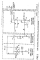
- a current switch logic circuit is shown with first and second terminals respectively connected to the bases of transistors T, and T 2 .
- the collector load resistor R, of the current switch is arranged to give the maximum collector swing without saturating the input transistor.
- the current switch output collectors, T, and T 2 are connected to an emitter follower level shifter circuit that drops the collector voltage swing to the most negative supply voltage, -2.2V, generating the base drive current for the high voltage output stage.
- the emitter-follower level shifter circuit may, as shown in Figure 1, be comprised of the serial connection of transistor TE, diode connected transistor TD, Schottky diode D 2 and resistor R 3 .
- the base of transistor TE is connected to the collectors of transistors T, and T2.
- the output from the emitter-follower level shifter circuit is taken from the juncture of Schottky diode D 2 and resistor R 3 .
- the open collector driver and output pad are on a first chip (CHIP ONE) whereas the terminating circuit (shown in the drawing as a terminating resistor RT is on a second chip (CHIP TWO).
- the open collector driver, the terminating circuit and the output pad could be on the same chip.
- the current through the transistor T 11 SBD clamp flows through the resistor R s in series with the base, causing a voltage drop to the base of transistor T,,. As the pad voltage drops, the SBD drags the base down and the emitter of transistor T,, will drop. The emitter of transistor T 11, or the collector of transistor T,o, will continue to drop until the anti-saturation SBD clamp on transistor T,o begins to conduct.
- the collector of transistor T has moved 3.2V with a maximum of 2.2V appearing across the devices.
- Fig. 2 In reference to the schematic diagram, Fig. 2; the operation is similar to that shown in Fig. 1. The difference is the introduction of diode connected transistor TL connected in parallel to the base-emitter junction of T,o.
- the emitter of TL is connected to the emitter of T,o and the base and collector of TL are connected to the base to T,o.
- This establishes the well known current mirror configuration where the emitter current to T,o is limited to some multiple of the emitter current of TL as determined by the ratio of the emitter area of T,o to the emitter area of TL.
- This provides for current limiting and over current protection of the output transistors T,. and T,, in the event that the chip output pad is inadvertently shorted to a power supply voltage.
- a third series transistor, T, 2 has been connected into the high voltage output stage.
- the chip pad is connected to the collector of T 1z .
- the off chip pad is connected to a terminator resistor connected in turn to a higher source of potential (+2.8V).
- the emitter of T, 2 is connected to the collector of T,,.
- the emitter of T, is connected to the collector of T,o.
- the emitter of T,o is connected to a source of potential (-2.2V).
- the base of T, 2 is connected to a source of reference potential (+1.4V) via a resistor R7.
- Resistor R8 connects the emitter of T, 2 to the source of reference potential (+1.4V).
- the base of T is connected to a source of reference potential (0.0V) via a resistor R 5 .
- Resistor R 6 connects the emitter of T,, to the source of reference potential (0.0V).
- the base of T,o is connected via resistor R4 to the output of the emitter follower level shifter. A total of 5V appears across the series connected output transistors.
- transistor T,o results in the activation of transistors T 11 and T,2, drawing current from the terminator resistor connected to the output pad.
- the pad voltage will drop, activating in turn the anti-saturation SBD clamps on the output transistors T, 2 , T,, and T 10 until and the output of the driver, the collector of T 12 , has moved 4.4V with a maximum of 2.2V appearing across any device. The same thing happens in reverse for turn-off.
- the number of series connected transistors is not limited to the two or three described herein, but that the transistors may be connected in this manner in series in a sufficient number to provide for arbitrarily large output voltage swings while limiting the voltage appearing across any one of them.
- Figure 4 In reference to the idealized waveforms, Figure 4, to be viewed in conjunction with the high voltage swing open collector driver of Figure 1; the input signal applied to the base of transistor T, is shown switching around 0V. This causes the output, the collector of T, to switch while maintaining voltage division across the output transistors T,, and T 10 as shown by the T,o collector waveform.
- the power supply voltage VCC and VEE are shown for reference.
- Figure 5 In reference to the idealized waveforms, Figure 5, to be viewed in conjunction with the wave form of Figure 4; the actual base-emitter voltage and the base-collector voltage for the series output transistors T,o and T, are shown illustrating the maintenance of the voltage division during the switching interval.
- the high voltage swing open collector driver need not be driven by a shifted emitter follower signal level out of a current switch logic circuit.
- the output series transistors, T,o and T,, are driven by a TTL type logic gate.
- the collector of the input TTL transistors T, and T 2 are connected to the base of the series output transistor T,o.
- the input logic signals, applied to the emitters of the input transistors T, and T 2 cause the input transistors to become active in either the normal or the inverse mode. When the input transistors are active in the normal mode, there is no base current into the series output transistor T,o.
Landscapes
- Engineering & Computer Science (AREA)
- Power Engineering (AREA)
- Physics & Mathematics (AREA)
- Computer Hardware Design (AREA)
- Computing Systems (AREA)
- General Engineering & Computer Science (AREA)
- Mathematical Physics (AREA)
- Logic Circuits (AREA)
- Electronic Switches (AREA)
Applications Claiming Priority (2)
| Application Number | Priority Date | Filing Date | Title |
|---|---|---|---|
| US855994 | 1986-04-25 | ||
| US06/855,994 US4677312A (en) | 1986-04-25 | 1986-04-25 | High voltage swing open collector driver |
Publications (3)
| Publication Number | Publication Date |
|---|---|
| EP0242651A2 true EP0242651A2 (de) | 1987-10-28 |
| EP0242651A3 EP0242651A3 (en) | 1990-01-10 |
| EP0242651B1 EP0242651B1 (de) | 1993-02-10 |
Family
ID=25322639
Family Applications (1)
| Application Number | Title | Priority Date | Filing Date |
|---|---|---|---|
| EP87104810A Expired - Lifetime EP0242651B1 (de) | 1986-04-25 | 1987-04-01 | Einen Treiber mit offenem Kollektor und hoher Spannungsauswanderung enthaltende integrierte Schaltung |
Country Status (4)
| Country | Link |
|---|---|
| US (1) | US4677312A (de) |
| EP (1) | EP0242651B1 (de) |
| JP (1) | JPH07101842B2 (de) |
| DE (1) | DE3784090T2 (de) |
Families Citing this family (5)
| Publication number | Priority date | Publication date | Assignee | Title |
|---|---|---|---|---|
| NL8702781A (nl) * | 1987-11-20 | 1989-06-16 | Philips Nv | Geintegreerde logische schakeling met "hot-carrier-stress"-reduktie en instabiliteiten-demping. |
| DE68924426T2 (de) * | 1989-10-26 | 1996-05-02 | Ibm | Selbstreferenzierte Stromschaltungslogik mit Push-Pull-Ausgangspuffer. |
| US5302864A (en) * | 1990-04-05 | 1994-04-12 | Kabushiki Kaisha Toshiba | Analog standard cell |
| US5241223A (en) * | 1992-05-12 | 1993-08-31 | International Business Machines Corporation | NORi circuit/bias generator combination compatible with CSEF circuits |
| US6104229A (en) | 1996-05-02 | 2000-08-15 | Integrated Device Technology, Inc. | High voltage tolerable input buffer and method for operating same |
Family Cites Families (14)
| Publication number | Priority date | Publication date | Assignee | Title |
|---|---|---|---|---|
| US3769524A (en) * | 1972-06-27 | 1973-10-30 | Ibm | Transistor switching circuit |
| US4065683A (en) * | 1974-06-12 | 1977-12-27 | Square D Company | Circuitry for industrial logic systems |
| US3962590A (en) * | 1974-08-14 | 1976-06-08 | Bell Telephone Laboratories, Incorporated | TTL compatible logic gate circuit |
| US3974402A (en) * | 1975-03-26 | 1976-08-10 | Honeywell Information Systems, Inc. | Logic level translator |
| JPS525254A (en) * | 1975-07-02 | 1977-01-14 | Hitachi Ltd | High voltage resistance mis switching circuit |
| US4070600A (en) * | 1976-12-23 | 1978-01-24 | General Electric Company | High voltage driver circuit |
| US4251737A (en) | 1978-12-29 | 1981-02-17 | International Business Machines Corporation | Dottable active collector driver circuit |
| US4296336A (en) | 1979-01-22 | 1981-10-20 | General Semiconductor Co., Inc. | Switching circuit and method for avoiding secondary breakdown |
| JPS5755333A (en) * | 1980-09-19 | 1982-04-02 | Sanyo Electric Co Ltd | Utilizing system of hot drainage |
| US4429237A (en) * | 1981-03-20 | 1984-01-31 | International Business Machines Corp. | High voltage on chip FET driver |
| JPS58116759A (ja) * | 1981-12-29 | 1983-07-12 | Fujitsu Ltd | 出力ドライバ回路 |
| US4508978A (en) * | 1982-09-16 | 1985-04-02 | Texas Instruments Incorporated | Reduction of gate oxide breakdown for booted nodes in MOS integrated circuits |
| US4585953A (en) * | 1983-07-20 | 1986-04-29 | International Business Machines Corporation | Low power off-chip driver circuit |
| US4584490A (en) * | 1984-03-30 | 1986-04-22 | Signetics Corporation | Input circuit for providing discharge path to enhance operation of switching transistor circuits |
-
1986
- 1986-04-25 US US06/855,994 patent/US4677312A/en not_active Expired - Fee Related
-
1987
- 1987-03-24 JP JP62068171A patent/JPH07101842B2/ja not_active Expired - Lifetime
- 1987-04-01 DE DE8787104810T patent/DE3784090T2/de not_active Expired - Fee Related
- 1987-04-01 EP EP87104810A patent/EP0242651B1/de not_active Expired - Lifetime
Also Published As
| Publication number | Publication date |
|---|---|
| DE3784090T2 (de) | 1993-08-12 |
| EP0242651B1 (de) | 1993-02-10 |
| US4677312A (en) | 1987-06-30 |
| EP0242651A3 (en) | 1990-01-10 |
| JPS62257217A (ja) | 1987-11-09 |
| DE3784090D1 (de) | 1993-03-25 |
| JPH07101842B2 (ja) | 1995-11-01 |
Similar Documents
| Publication | Publication Date | Title |
|---|---|---|
| US4494016A (en) | High performance MESFET transistor for VLSI implementation | |
| KR950005023B1 (ko) | Ecl게이트의 전력소비를 변화시키는 장치 및 ecl회로를 동작시키는 방법 | |
| US4806796A (en) | Active load for emitter coupled logic gate | |
| US4616146A (en) | BI-CMOS driver circuit | |
| US6040729A (en) | Digital output buffer for multiple voltage system | |
| EP0480201A1 (de) | Chip-Ausgangsschnittstellenschaltung | |
| US3551693A (en) | Clock logic circuits | |
| US4638186A (en) | BIMOS logic gate | |
| GB1358193A (en) | Integrated control circuit | |
| EP0250947A2 (de) | Logisches Tor vom Bimos-Typ | |
| US3699362A (en) | Transistor logic circuit | |
| EP0231667A2 (de) | Ausgangspufferschaltungen | |
| JPH02222216A (ja) | BiCMOSドライバ回路 | |
| US3660675A (en) | Transmission line series termination network for interconnecting high speed logic circuits | |
| KR900000487B1 (ko) | 논리 게이트 회로 | |
| US4496856A (en) | GaAs to ECL level converter | |
| EP0018739B1 (de) | Dekodierschaltung für eine Halbleiterspeichervorrichtung | |
| EP0242651B1 (de) | Einen Treiber mit offenem Kollektor und hoher Spannungsauswanderung enthaltende integrierte Schaltung | |
| EP0055341B1 (de) | Stromgesteuertes Gatter | |
| EP0110916B1 (de) | Logische schaltung mit stromgesteuerten anreicherungsfeldeffekttransistoren | |
| US4488064A (en) | Integrated circuit with a common power supply for silicon and gallium arsenide circuit portions | |
| US5077490A (en) | Schottky-diode emulator for BiCMOS logic circuit | |
| US4868904A (en) | Complementary noise-immune logic | |
| US5661411A (en) | Feedback controlled load logic circuit | |
| US5546040A (en) | Power efficient transistor and method therefor |
Legal Events
| Date | Code | Title | Description |
|---|---|---|---|
| PUAI | Public reference made under article 153(3) epc to a published international application that has entered the european phase |
Free format text: ORIGINAL CODE: 0009012 |
|
| AK | Designated contracting states |
Kind code of ref document: A2 Designated state(s): DE FR GB IT |
|
| 17P | Request for examination filed |
Effective date: 19880224 |
|
| PUAL | Search report despatched |
Free format text: ORIGINAL CODE: 0009013 |
|
| AK | Designated contracting states |
Kind code of ref document: A3 Designated state(s): DE FR GB IT |
|
| 17Q | First examination report despatched |
Effective date: 19900727 |
|
| GRAA | (expected) grant |
Free format text: ORIGINAL CODE: 0009210 |
|
| AK | Designated contracting states |
Kind code of ref document: B1 Designated state(s): DE FR GB IT |
|
| PG25 | Lapsed in a contracting state [announced via postgrant information from national office to epo] |
Ref country code: IT Free format text: LAPSE BECAUSE OF FAILURE TO SUBMIT A TRANSLATION OF THE DESCRIPTION OR TO PAY THE FEE WITHIN THE PRESCRIBED TIME-LIMIT;WARNING: LAPSES OF ITALIAN PATENTS WITH EFFECTIVE DATE BEFORE 2007 MAY HAVE OCCURRED AT ANY TIME BEFORE 2007. THE CORRECT EFFECTIVE DATE MAY BE DIFFERENT FROM THE ONE RECORDED. Effective date: 19930210 |
|
| REF | Corresponds to: |
Ref document number: 3784090 Country of ref document: DE Date of ref document: 19930325 |
|
| ET | Fr: translation filed | ||
| PLBE | No opposition filed within time limit |
Free format text: ORIGINAL CODE: 0009261 |
|
| STAA | Information on the status of an ep patent application or granted ep patent |
Free format text: STATUS: NO OPPOSITION FILED WITHIN TIME LIMIT |
|
| 26N | No opposition filed | ||
| PGFP | Annual fee paid to national office [announced via postgrant information from national office to epo] |
Ref country code: FR Payment date: 19950328 Year of fee payment: 9 |
|
| PGFP | Annual fee paid to national office [announced via postgrant information from national office to epo] |
Ref country code: DE Payment date: 19950428 Year of fee payment: 9 |
|
| PGFP | Annual fee paid to national office [announced via postgrant information from national office to epo] |
Ref country code: GB Payment date: 19960325 Year of fee payment: 10 |
|
| PG25 | Lapsed in a contracting state [announced via postgrant information from national office to epo] |
Ref country code: FR Effective date: 19961227 |
|
| PG25 | Lapsed in a contracting state [announced via postgrant information from national office to epo] |
Ref country code: DE Effective date: 19970101 |
|
| REG | Reference to a national code |
Ref country code: FR Ref legal event code: ST |
|
| PG25 | Lapsed in a contracting state [announced via postgrant information from national office to epo] |
Ref country code: GB Effective date: 19970401 |
|
| GBPC | Gb: european patent ceased through non-payment of renewal fee |
Effective date: 19970401 |