EP0244105A2 - Structures capacitives intégrés dans des composants aux micro-ondes à lignes à ailettes - Google Patents
Structures capacitives intégrés dans des composants aux micro-ondes à lignes à ailettes Download PDFInfo
- Publication number
- EP0244105A2 EP0244105A2 EP87303087A EP87303087A EP0244105A2 EP 0244105 A2 EP0244105 A2 EP 0244105A2 EP 87303087 A EP87303087 A EP 87303087A EP 87303087 A EP87303087 A EP 87303087A EP 0244105 A2 EP0244105 A2 EP 0244105A2
- Authority
- EP
- European Patent Office
- Prior art keywords
- metallization layer
- metallization
- margin
- waveguide
- channel region
- Prior art date
- Legal status (The legal status is an assumption and is not a legal conclusion. Google has not performed a legal analysis and makes no representation as to the accuracy of the status listed.)
- Granted
Links
Images



Classifications
-
- H—ELECTRICITY
- H01—ELECTRIC ELEMENTS
- H01P—WAVEGUIDES; RESONATORS, LINES, OR OTHER DEVICES OF THE WAVEGUIDE TYPE
- H01P3/00—Waveguides; Transmission lines of the waveguide type
- H01P3/02—Waveguides; Transmission lines of the waveguide type with two longitudinal conductors
- H01P3/023—Fin lines; Slot lines
Definitions
- This invention relates to microwave finline devices for signal detection and the like and more particularly to millimeter wave finline structures using integrated capacitor technology.
- the invention is particularly useful for detection for microwave energy having a fundamental frequency of above about twenty-five GHz.
- waveguide detection devices have employed precision machined conventional waveguide technology.
- accuracy of machining of parts becomes of critical importance with shorter wavelengths of interest.
- wavelengths of interest include those on the order of five (5) mm. at about sixty (60) GHz.
- a significant problem with detectors for such high frequencies and short wavelengths is inherently poor impedance match between detection diodes and the waveguide, which results in loss of power as represented by a VSWR as great as 3:1.
- Other problems will be apparent hereinafter.
- Figure 1 herein represents a finline structure 10 reconstructed from the brief description in the prior art Gol et al. paper. It shows a dielectrically loaded finline circuit 12 on a quartz dielectric substrate 14 in a waveguide 16. (Interior waveguide boundaries are shown partially in phantom. In the cited publication, surface and waveguide boundaries are not illustrated.)
- Metallization layers 18, 19 on the front surface 21 of the dielectric substrate 14 are shown to be provided, the layers 18, 19 having in surface pattern an input taper 20 and an output taper 22.
- Metallization layer 18 is presumed to be in d.c. contact with the waveguide 16, and metallization layer 19 is presumed to be d.c. isolated from the waveguide 16. Detected signals are presumably obtained from metallization 19.
- Matching the impedance of a free-space waveguide to a finline structure is important.
- Various techniques have been proposed. For example, quarter-wave transition matching transformers have been proposed. Such a technique is discussed in Verver et al., "Quarter-Wave Matching of Waveguide-to-Finline Transitions," IEEE Transactional on Microwave Theory and Techniques , Vol. MTT-32, No. 12, December 1984, pp. 1645-1647. Therein it is suggested that the transition from free space to dielectric loading of the waveguide cannot be reflectionless because of the discontinuity introduced by the dielectric.
- the proposed solution namely a quarter-wave matching stub extending along the waveguide axis into the free-space waveguide from the finline structure, provides an inherently narrow frequency match. There is thus a need for a solution which offers broadband impedance matching.
- the present invention is directed to advancing the state of finline technology to increase versatility and usefulness over the art heretofore known.
- a finline structure comprises a dielectric substrate-mounted circuit disposed within a millimeter waveguide, said substrate circuit comprising a substrate having a surface sufficiently smooth to support integrated distributed capacitance elements of predefinable characteristics, and distributed capacitance elements being at least partially formed by laterally separated metallization layers.
- the distributed capacitance elements permit the biasing of a plurality of circuit elements in finline transmission medium.
- r.f. continuity is effected between traces and metallization layers while maintaining d.c. isolation.
- Examples of circuits which can incorporate an integrated capacitor include but are not limited to detectors, r.f. modulators, r.f. attenuators, amplifiers, and multipliers.
- a detector is defined wherein the metallization layers form, together with the dielectric substrate, a pattern defining a shorting stub-type matching termination, an impedance matching network with exponential taper, and a detection region.
- a discrete (non-integrated) diode is mounted at the narrowest juncture in the detection region (the finline gap) thereby defining a detection site.
- Structures including a metallization layer, dielectric layer, a metallization bridge layer and the substrate define distributed capacitances built into the matching network.
- the leading edge of the dielectric substrate as mounted in a waveguide may be shaped in a gradual taper to form a broadband transition from a free-space waveguide to a dielectrically loaded waveguide.
- Other structures incorporating the invention are constructed in a similar fashion with bias connections through traces leading to terminals external to the waveguide in which the subject finline structure is mounted.
- a detector according to the invention provides for minimum reflections and maximum energy transfer at the detection site.
- the structure is readily fabricated employing photolithographic techniques.
- Circuits constructed according to the invention are not limited in bias options to uniform bias or to only two-terminal circuit elements.
- a plurality of elements, as well as multiple port elements, may be selectively biased while retaining d.c. isolation and r.f. continuity.
- the versatility of construction allows for higher levels of integration as well as the realization of new topologies previously unattainable. Since the capacitance structure is integrated into the thin film circuit, fewer discrete parts are required and the manufacturing process may be precisely controlled by photolithography.
- Figure 1 depicts one suggestion in the published literature of a finline detection device.
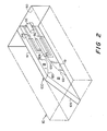
- Figures 2 through 11 illustrate embodiments of the present invention.
- FIG 2 there is shown a finline structure 100 mounted within the interior boundaries of a waveguide 16.
- a typical waveguide 16 is a Type WR-19 waveguide designed for a center frequency of 50 GHz with a design operating frequency range of 40 GHz to 60 GHz.
- the present invention is not solely limited to this range of operation as other structure sizes and frequencies ranges can have the same basic features or produce the same basic conditions characteristic of the present invention.
- the interior cross-sectional dimension of a standard WR-19 waveguide is 2.39 mm height by 4.78 mm width.
- a finline circuit 100 is formed on a dielectric substrate 14 with at least one integrated distributed capacitance element 42 or 44 wherein a dielectrically insulated bridge is provided along a gap 56 or 66 separating metallization layers 18,118 or 19, 118.
- the finline circuit according to the invention is mounted within the waveguide 16 extending between interior walls in the narrower (height) dimension, with a junction element 124 mounted to metallization layers 18, 19, 118 of the finline circuit 100.
- Metallization layers 18, 19 and 118 on the front surface 21 of the dielectric substrate 14 are provided in a specific example such that the metallization layers 18, 19 define input tapers 120, 122 in surface pattern on the substrate and layer 118 define a slot 30 of dielectric material exposed in the waveguide 16.
- the slot 30 forms a matching stub of predefined length along the front surface 21.
- junction element 124 is a matching network as explained in connection with Figure 3.
- the leading edge of dielectric substrate 100 is a leading edge taper 126 to introduce a smooth impedance transition from a free-space waveguide to a dielectrically-loaded waveguide of a relatively high dielectric coefficient.
- the leading edge taper defines a gradual transition along the length of the waveguide 16 from one wall to the opposing wall.
- the leading edge taper 126 is preferably tapered from zero waveguide height to maximum waveguide height at an angle not exceeding thirty (30) degrees.
- a straight taper is simple and convenient for manufacturing purposes, and it provides for orderly impedance transition and improved reflection coefficient for the finline circuit.
- the thickness of the dielectric substrate 14 is selected to be on the order of 0.25 mm. This thickness is consistent with the preferred thickness of a simple dielectric sheet in a dielectrically-loaded waveguide designed to operate at about 50 GHz.
- the dielectric substrate 100 is preferably a smooth or even polished material, and preferably the dielectric substrate 100 is formed of sapphire or fused silica quartz.
- the dielectric constant may be on the order of 3.8.
- the metallization layers 18, 19 and 118 may be formed of any highly conductive material which will bind to the surface of the material forming the substrate 100.
- the metallization layers may be formed of gold or silver. Gold is preferred due to its high conductivity and its corrosion resistance.
- a detected signal must be extracted from the waveguide 16.
- the metallization layer 118 is d.c. coupled to an output probe 32 through a rear wall 50 of the waveguide 16.
- Metallization layer 118 is d.c. isolated from the waveguide 16.
- the metallization layers 18 and 19 each define curvilinear tapers 120 and 122, respectively, on the front surface 21 of the dielectric substrate 14.
- the metallization layers together define a transition region from maximum dielectric exposure (wall to wall in the waveguide 16) upstream of the detection region 123 to minimum dielectric exposure at the detection region 123.
- the minimum separation between metallization layer 18 and metallization layer 19 is preferably about 0.15 mm at the detection region 123.
- the value L may be chosen, for example, to be sufficiently large such that values of z representing greater than 1.3 wavelengths do not differ significantly from a metallization profile parallel with the waveguide axis downstream of the detection region 123.
- the slot 30 downstream of the detection region 123 may preferably be formed of straight parallel opposing margins of the metallization layers along the axis of the waveguide.
- the detection means 124 as shown in Figure 3 preferably comprises a hybrid chip component carrier 38 containing a low-barrier or a zero-bias Schottky diode 24 for detection and a lumped-element resistor 34 for impedance matching.
- An optional lumped-element capacitor 36 may be optionally provided in the component carrier 38. The value is included with the intrinsic capacitance of the the carrier 38 at the gap formed between metallization layers 19 and 118. The purpose of capacitor 36 is to maintain d.c. voltage on the d.c.-isolated metallization layer 118 to permit voltage detection of an r.f. signal.
- the component carrier 38 may be mounted to the substrate surface 21 by conventional mounting techniques.
- the diode 24 is mounted with its cathode terminal coupled to metallization layer 18 and with its anode terminal coupled to metallization layer 118 in a region less than approximately one-quarter wavelength electric distance d (at 50 GHz) from the backshort termination 40. It is the slot 30 which defines the backshort to the dielectric substrate 14 of up to approximately one-quarter wavelength in electrical length.
- the purpose of the backshort and its choice of length is as follows:
- the diode 24 exhibits intrinsic junction capacitance which must be counteracted if detection sensitivity is not to degrade with changing wavelengths of operation.
- One purpose of the backshort formed by slot 30 is to provide a shunt inductance across the intrinsic junction capacitance.
- the proper shunt inductance appears across the intrinsic junction capacitance at intended operating frequencies when the length d of the backshort is slightly less than about one-quarter wavelength, as measured from the position of a terminal of diode 24 to the backshort termination 40 of the slot 30.
- the added shunt inductance tends to improve waveguide to detector matching and to improve the flatness of detector frequency response.
- the lumped element resistor 34 of the detection means 124 provides a needed resistive match for detection. Without the resistor 34, the input match is otherwise a strong function of input power to the finline structure 100.
- the lumped element resistor 34 which is typically of a value of about 250 Ohm, appears in shunt across the detection diode 24 and is thus in shunt with the characteristic video impedance of the diode 24. Values for the lumped element resistor 34 are chosen for optimum detection sensitivity and match between the waveguide and the finline detector.
- distributed capacitances are formed directly on the surface 21 of the finline structure 100.
- the distributed capacitances provide r.f. coupling with d.c. isolation for purposes such as detector voltage storage, selectively controlled biasing and many other applications.
- the versatility afforded by distributed capacitance structures are particularly advantageous at microwave frequencies because photolithographic techniques can be employed to form precisely-controlled integrated structures. Details of an exemplary distributed capacitance structure are described in connection with Figure 4.
- Capacitor 42 is formed along facing portions 52 and 54 of respective metallization layers 18 and 118 along a slit 56 together with dielectric layers 58 underlying the slit 56, as hereinafter explained.
- the slit 56 extends from the region of the slot 30 adjacent the detection region 123 to the rear wall 50.
- the lateral boundaries 44A and 44B of typical capacitor 44 are outlined in phantom and are similarly designated in Figure 4.
- the entire capacitor 42 extends from the gap region 70 toward the rear wall 50 along the slit 56.
- the entire capacitor 44 extends from the gap region 72 toward the rear wall 50 along the slit 66.
- the materials forming the distributed capacitors 42 and 44 are mounted via thin-film techniques over an area of the surface 21.
- FIG 4 there is shown a side cross-sectional view (along lines 4-4 of Figure 3) of a typical distributed capacitor 44 in accordance with the invention.
- the ratio of vertical to planar dimensions is highly exaggerated for illustration purposes.
- Typical thicknesses of the layers are in the sub-micrometer range.
- the distributed capacitance means 44 is photolithographically formed in thin film on dielectric substrate 14 in layers of the following composition: A base metallization layer 80 of for example tantalum directly upon the substrate 14 within the boundaries of capacitor 44, as indicated in phantom; the base layer 80 being oxidized to form an intermediate layer 82 of tantalum pentoxide, likewise within the boundaries of capacitor 44, but completely covering the base layer 80; a thin-film stratum 84 forming the dielectric bridging under metallization layers 118 and 19; the thin-film dielectric stratum being of for example silicon dioxide; and metallization strata 86 (of tantalum nitride), 88 (of chrome) and 87 or 89 (of gold) defining the metallization layers 118 or 19.
- a base metallization layer 80 of for example tantalum directly upon the substrate 14 within the boundaries of capacitor 44, as indicated in phantom; the base layer 80 being oxidized to form an intermediate layer 82 of tantalum pentoxide, likewise within the boundaries
- Chrome is of particular importance as an adhesion layer between the layers of gold and tantalum nitride. Tantalum nitride binds with silicon dioxide but not with gold. Chrome binds with both tantalum nitride and gold and is therefore a suitable adhesion medium.
- the slit 66 is formed through layers 86, 88 and the metallization layers (118 or 19) to the layer 84 of silicon dioxide. Each of these layers is applied by thin-film photolithographic techniques, a procedure believed to be new among microwave finline structures.
- Figure 5 is a schematic of an approximate equivalent circuit of the finline structure 100 of Figure 2, together with a signal source 200 and source resistance 202.
- Impedance matching resistor 34 represents the resistance required for a good match between the loaded waveguide and the detector defined by structure 100.
- the input resistance is shunted across the input to the structure 100.
- Diode 24 is a.c. coupled to ground through capacitor 44 and a.c. coupled to a termination element (slot 30) though capacitor 42.
- a current path is provided between the anode of diode 24 and the output terminal 32.
- the termination element 30 comprises the equivalent of a delay line 130 having as a termination an inductive load 132.
- the inductive load is coupled across the unbalanced termination of the delay line 130.
- the unbalanced side of the delay line 130 is coupled to the anode of the diode 24 to provide a complete rectified a.c. signal path through the diode 24 and inductor 132.
- the detectable signal is derived from this signal path. It is to be understood that modeling of a finline circuit is not precise due to the nature of the structure and the signal paths.
- the inductor-diode signal loop for example represents the current flow path around the slot 30 in the metallization layer 118.
- an a.c. e.g., sinusoidal
- the nonlinear element namely the low barrier diode 24 will conduct current in a sense or direction such that a d.c. voltage will appear on the metallization layer 118.
- the capacitances 42 and 44 provide an r.f. signal path through the metallization layer 118.
- a capacitor such as optional capacitor 36 of Figure 3 or distributed capacitor 44, serves to maintain the d.c.
- Signals may be picked off at the probe output terminal 32 and supplied to a buffer amplifier (not shown) for processing.
- FIG. 6 there is shown a perspective view of a finline structure illustrating construction of a simple biasing configuration.
- a finline substrate 140 is mounted within and between opposing first and second (grounded) mating metal halves 160, 162 of means forming free-space waveguide 16 to place a finline circuit 200 within the waveguide 16
- Fourth metallization region 228 includes a stem 216 is d.c. isolated from the waveguide 16. To assure proper isolation of the stem 216 from the waveguide half 162, the second waveguide half 162 is provided with a relief 164 aligned with the stem 216 and which is at least as wide as the combined width of the stem 216 and the channels 212 and 214.
- the distributed capacitance 44 provides sufficient r.f. continuity such that the transmission slot (first channel 210) appears in the circuit as an unperturbed unilateral finline, despite the presence of a d.c. bias.
- d.c. bias may be applied externally to the pad 228 from a d.c. source connected to the stem 216.
- a quarter-wave slot 130 may be provided which has a backshort 240 at the quarter wave position of the multiplied frequency, for example, three times the fundamental frequency 3f o .
- Output of the multiplier circuit 300 into a surrounding waveguide cavity (as in Figure 2) containing the finline circuit is via the finline channel defined by a first channel 310 along the axis 301 of the waveguide.
- FIG 8 there is shown a further embodiment of a finline detector 400 similar in topology to the finline detector circuit 100 of Figure 3.
- the circuit is formed on a dielectric substrate 21, and a finline slot 30 is disposed in line with a waveguide central axis 301 within a surrounding waveguide.
- the finline slot 30 terminates in a quarter-wave backshort 40 formed in metallization layer 18.
- a matching resistance means 134 is provided across finline slot 30 between first metallization layer 18 and second metallization layer 19.
- the matching resistance means may be a discrete resistor as in the embodiment of Figure 3, or it may be a thin film resistor of for example tantalum nitride printed on the finline substrate and spanning the finline slot 30.
- a diode detector 224 is coupled across the finline slot 30 between first metallization layer 18 and d.c.-isolated third metallization layer 118.
- the third metallization layer 118 forms a trace between first and second dielectric channels 56 and 66.
- a thin-film capacitance means 44 is provided on the finline substrate 21 bridging first and second dielectric channels 56 and 66 and in r.f. contact with first metallization layer 18 (at region 18A), third metallization layer 118 (at region 118A), and second metallization layer 19 (at region 19A), thereby to provide for r.f. coupling between first and third metallization layers 18 and 118 and between second and third metallization layers 19 and 118.
- Detection of signals is provided at any point along the third metallization layer 118, preferably at an external terminal 121 remote from the finline slot 30. Further, according to the invention, a d.c. bias may be applied through the external terminal 121 thereby to set a desired level of signal detection. The ability to provide d.c. bias in this manner in a finline circuit represents added flexibility and advantage.
- incoming r.f. signals along axis 301 are detected by the diode 224, and the capacitance means 44 provide r.f. continuity across the the metallization layers 18, 118 and 19 as well as provide a d.c. holding capacitance for voltage detected across the diode 224.
- FIG. 9 illustrates another application of the invention, namely, a microwave modulator 500.
- the microwave modulator 500 has an input port 504 for unmodulated r.f. signals and an output port 505 for modulated r.f. signals along a waveguide axis 301.
- first, second and third P.I.N. diodes 501, 502 and 503 are coupled across a finline through-slot 230 between common metallization layer 18 and respective first, second and third terminal pads 506, 508 and 510.
- the terminal pads are separated by metallization layers 19, 219, 319 and 419, which are also on the side of the finline through-slot 230 opposite the common metallization layer 18.
- the pads 506, 508 and 510 are respectively d.c.-isolated from the adjacent metallization layers by dielectric channels 512, 513; 514, 515; and 516, 517.
- the pads 506, 508 and 510 are coupled, respectively with traces 507, 509 and 511 between the dielectric channels.
- a distributed capacitance means 44 adjacent the finline through-slot 230 to bridge the metallization layers 19, 219, 319 and 419 and the adjacent pads 506, 508 and 510, thereby to provide r.f. signal continuity along the finline through-slot 230. Because each of the P.I.N.
- the traces 507, 509 and 511 are advantageously provided with d.c. biasing V1, V2 and V3 of independent level and conditions. Independent biasing allows improved modulator match, greater dynamic range and broader or flatter response operational frequency range to an extent not attainable in any prior known finline modulator.
- FIG. 10 illustrates a still further application of the invention, namely a finline stepped attenuator 600.
- the stepped attenuator 600 comprises a finline through-slot 230 for unattenuated r.f. input at the input end 604 and selectively attenuated r.f. output at the output end 605.
- a first metallization layer 18 is provided on one side of the finline through-slot 230.
- First, second and third slotline gaps 330, 430 and 530 are disposed transverse to and along the finline through-slot 230.
- the slotline gaps 330, 430 and 530 are preferably at right angles to the finline through-slot 230.
- the slotline gaps 330, 430 and 530 are preferably provided with respective energy absorption means 134, 234, and 334, such as lossy tantalum nitride.
- first, second and third diodes 601, 602 and 603 are coupled across the respective slotline gaps 330, 430 and 530 along finline through-slot 230 between metallization layers 219, 319, and 419 and pads 606, 608 and 610 opposing first metallization layer 18 across the finline through-slot 230.
- the terminal pads 606, 608 and 610 are separated from metallization layers 19, 219, 319 and 419 and are thus respectively d.c.-isolated from the adjacent metallization layers by dielectric channels 612, 613; 614, 615; and 616, 617.
- the pads 606, 608 and 610 are coupled, respectively, with traces 607, 609 and 611 between the dielectric channels.
- distributed capacitance means 144, 244 and 344 adjacent the finline through-slot 230 to bridge the metallization layer 19 to pad 606 and to metallization 219, to bridge metallization layer 219 to pad 608 and to metallization layer 319, and to bridge metallization layer 319 to pad 610 and to metallization layer 419.
- Each of the pads 606, 608 and 610 is disposed on one side only of the slotline gaps 330, 430 and 530, thereby to provide r.f. signal continuity selectively along the finline through-slot 230.
- the diodes 601, 602 and 603 when in the on state provide relatively low loss r.f. continuity bypassing and effectively shorting out the lossy transmission line segments provided by the slotline gaps 330, 430 and 530. Because each of the diodes 601, 602 and 603 is d.c.-isolated from one another and the metallization layers 19, 219, 319 and 419, then the traces 607, 609 and 611 and thus diodes 601, 602 and 603 can be independently and advantageously provided with d.c.
- V1, V2 and V3 biasing V1, V2 and V3 to turn the diodes 601, 602, 603 on or off.
- the slotline gap 330, 430 and 530 appears in the finline circuit 600 as a lossy transmission line in series with the finline through-slot 230.
- the slotline gap does not appear in the finline circuit 600 because the r.f. energy is shunted through the diodes bypassing the lossy transmission lines and avoiding attenuation.
- Independent biasing allows stepped remote selectivity of attenuation level.
- the distributed capacitance 144, 244 or 344 provides the r.f. continuity across the dielectric channel 613, 615 or 617 and along the margin of slotline gap 330, 430 or 530 which is needed to support the electric field energy (E-field) in the slotline gap 330, 430 or 530.
- E-field electric field energy
- slotline gaps preferably not containing a lossy material
- the slotline gaps may be formed with appropriate lengths to act as wave traps in a frequency-selective band reject filter network.
- the filter characteristics can be changed by selectively biasing the diodes to the on or off states.
- FIG. 11 there is shown a plan view details of one embodiment of an r.f. amplifier 700 using finline technology according to the invention.
- a simplified model of a beam lead field effect transistor (FET) 728 having a gate G, a source S and a drain D, is mounted across a finline through-slot 230 between d.c.-isolated terminals.
- FET beam lead field effect transistor
- a metallization layer 18 serves as a terminal for source S
- a first pad 706 serves as a terminal for gate G
- a second pad 708 serves as a terminal for drain S.
- Metallization layers 19, 219 and 319 surround the pads 706 and 708, being d.c. separated by dielectric channels 712, 713, 714 and 715.
- r.f. continuity is provided through the metallization 19 and the first pad 706 to metallization 219 by first capacitance means 444 bridging channel 712 and channel 713. Further, r.f. continuity is provided between metallization 219, the second pad 708 and metallization 319 by second capacitance means 544 bridging the channel 714 and the channel 715. Still further according to the invention, a first trace 707 is provided for d.c. coupling the first pad 706 with a gate bias 731. A second trace 709 is provided for d.c. coupling the second pad 708 with a drain bias 732.
- a slotline gap 730 in series connection with the through-slot 230 separates the first pad 706 from the second pad 708 and extends outwardly from the finline through-slot 230 to define a quarter-wave termination.
- This quarter-wave termination consists of the parallel combination of slotline gap 730 and shorted slotline stub 733, which is defined by the metallization layer 219.
- the distributed capacitance 444 or 544 according to the invention provides the r.f. continuity across the dielectric channel 713 or 714 and along each (lateral) margin of the slotline gap 730 and the shorted slotline stub 733 which is needed to support the electric field energy (E-field) in the slotline gap 730 and slotline stub 733. Were there no r.f.
- slotline gap 730 and slotline stub 733 The parallel combination of slotline gap 730 and and slotline stub 733 is to provide a series shorted stub which acts as an impedance converter so as to cause the appearance of an open circuit at the the through-slot 230 where the active device 728 is positioned. This is necessary to provide electrical isolation between the input 704 and the output 705. Bias may be applied independently to the gate G through trace 707 and to the drain D through trace 709.
- the capacitance means 444 and 544 which may be thin film distributed capacitors, provide the necessary r.f. continuity to the finline amplifier circuit 700.
Landscapes
- Microwave Amplifiers (AREA)
- Waveguide Connection Structure (AREA)
Applications Claiming Priority (2)
| Application Number | Priority Date | Filing Date | Title |
|---|---|---|---|
| US06/852,861 US4789840A (en) | 1986-04-16 | 1986-04-16 | Integrated capacitance structures in microwave finline devices |
| US852861 | 1986-04-16 |
Publications (3)
| Publication Number | Publication Date |
|---|---|
| EP0244105A2 true EP0244105A2 (fr) | 1987-11-04 |
| EP0244105A3 EP0244105A3 (en) | 1989-02-08 |
| EP0244105B1 EP0244105B1 (fr) | 1992-08-12 |
Family
ID=25314423
Family Applications (1)
| Application Number | Title | Priority Date | Filing Date |
|---|---|---|---|
| EP87303087A Expired EP0244105B1 (fr) | 1986-04-16 | 1987-04-09 | Structures capacitives intégrés dans des composants aux micro-ondes à lignes à ailettes |
Country Status (4)
| Country | Link |
|---|---|
| US (1) | US4789840A (fr) |
| EP (1) | EP0244105B1 (fr) |
| JP (1) | JPH0783217B2 (fr) |
| DE (1) | DE3781010T2 (fr) |
Cited By (3)
| Publication number | Priority date | Publication date | Assignee | Title |
|---|---|---|---|---|
| EP0245048A3 (en) * | 1986-05-08 | 1988-10-05 | Hewlett-Packard Company | Finline millimeter wave detector |
| EP0735604A1 (fr) * | 1995-03-28 | 1996-10-02 | Murata Manufacturing Co., Ltd. | Ligne diélectrique planaire et circuit intégré l'utilisant |
| CN104538717A (zh) * | 2014-12-16 | 2015-04-22 | 东南大学 | 一种基片集成同轴线的尺寸设计方法 |
Families Citing this family (21)
| Publication number | Priority date | Publication date | Assignee | Title |
|---|---|---|---|---|
| US4980636A (en) * | 1989-08-10 | 1990-12-25 | The United States Of America As Represented By The Administrator, National Aeronautics And Space Administration | Universal nondestructive MM-wave integrated circuit test fixture |
| US5225796A (en) * | 1992-01-27 | 1993-07-06 | Tektronix, Inc. | Coplanar transmission structure having spurious mode suppression |
| US5232549A (en) * | 1992-04-14 | 1993-08-03 | Micron Technology, Inc. | Spacers for field emission display fabricated via self-aligned high energy ablation |
| US5528202A (en) * | 1992-08-27 | 1996-06-18 | Motorola, Inc. | Distributed capacitance transmission line |
| EP0607044B1 (fr) * | 1993-01-13 | 1999-08-11 | Honda Giken Kogyo Kabushiki Kaisha | Mélangeur à guide d'onde diélectrique et module radar à guide d'onde diélectrique |
| IT1284025B1 (it) * | 1996-06-18 | 1998-05-08 | Italtel Spa | Convertitore di frequenza per applicazioni alle onde radio millimetriche |
| US5920240A (en) * | 1996-06-19 | 1999-07-06 | The Regents Of The University Of California | High efficiency broadband coaxial power combiner/splitter with radial slotline cards |
| JP3067675B2 (ja) * | 1997-02-27 | 2000-07-17 | 株式会社村田製作所 | 平面誘電体集積回路 |
| RU2158044C2 (ru) * | 1998-12-30 | 2000-10-20 | Государственное научно-производственное предприятие "НИИПП" | Свч-модуль |
| US6384691B1 (en) * | 2000-03-15 | 2002-05-07 | Tlc Precision Wafer Technology, Inc. | Millimeter wave low phase noise signal source module |
| US6411494B1 (en) | 2000-04-06 | 2002-06-25 | Gennum Corporation | Distributed capacitor |
| WO2001082404A1 (fr) | 2000-04-20 | 2001-11-01 | Paratek Microwave, Inc. | Dephaseur accordable a guide d'onde et ligne a ailettes |
| EP1497758A1 (fr) * | 2002-04-18 | 2005-01-19 | University Of South Florida | Systeme universel de modelisation d'un circuit equivalent pour des elements de circuit montes sur un substrat integrant des caracteristiques dependantes du substrat |
| JP2007060127A (ja) * | 2005-08-23 | 2007-03-08 | Sony Corp | スロット・アンテナ |
| US20070133083A1 (en) * | 2005-12-07 | 2007-06-14 | Kangaslahti Pekka P | Waveguide apparatus with integrated amplifier and associated transitions |
| US7583074B1 (en) | 2005-12-16 | 2009-09-01 | Hrl Laboratories, Llc | Low cost millimeter wave imager |
| US20080112705A1 (en) * | 2006-11-13 | 2008-05-15 | Optimer Photonics, Inc. | Frequency selective mmw source |
| US8098185B2 (en) * | 2006-11-13 | 2012-01-17 | Battelle Memorial Institute | Millimeter and sub-millimeter wave portal |
| US8030913B1 (en) | 2008-07-14 | 2011-10-04 | Hrl Laboratories, Llc | Detector circuit with improved bandwidth |
| US8390403B1 (en) | 2009-01-26 | 2013-03-05 | Hrl Laboratories, Llc | Wideband ridged waveguide to diode detector transition |
| US11754444B2 (en) | 2021-03-19 | 2023-09-12 | Rockwell Collins, Inc. | Distributed integrate and dump circuit |
Family Cites Families (14)
| Publication number | Priority date | Publication date | Assignee | Title |
|---|---|---|---|---|
| JPS583401B2 (ja) * | 1972-05-23 | 1983-01-21 | 日本放送協会 | マイクロハカイロ |
| NL7609903A (nl) * | 1976-09-07 | 1978-03-09 | Philips Nv | Microgolfinrichting voor het omzetten van een golfpijp- in een microstripgeleiderstructuur. |
| US4291278A (en) * | 1980-05-12 | 1981-09-22 | General Electric Company | Planar microwave integrated circuit power combiner |
| US4425549A (en) * | 1981-07-27 | 1984-01-10 | Sperry Corporation | Fin line circuit for detecting R.F. wave signals |
| US4541120A (en) * | 1982-08-19 | 1985-09-10 | International Standard Electric Corporation | Transmitter-receiver module |
| GB2126429A (en) * | 1982-08-27 | 1984-03-21 | Philips Electronic Associated | R f balanced mixer |
| GB2126430A (en) * | 1982-08-27 | 1984-03-21 | Philips Electronic Associated | R f circuit arrangement |
| DE3315860A1 (de) * | 1983-04-30 | 1984-10-31 | Philips Patentverwaltung Gmbh, 2000 Hamburg | Mischer |
| DE3330099C2 (de) * | 1983-08-20 | 1985-11-21 | Hermann Dipl.-Ing. 7778 Markdorf Ebner | Hohlleiter/Mikrostrip Übergang |
| GB2147472A (en) * | 1983-09-30 | 1985-05-09 | Philips Electronic Associated | RF-solid-state arrangement |
| FR2560442B1 (fr) * | 1984-02-24 | 1987-08-07 | Thomson Csf | Dispositif de commutation et de limitation a ligne a fente, fonctionnant en hyperfrequences |
| GB2161990B (en) * | 1984-07-18 | 1987-08-19 | Philips Electronic Associated | Finline with dc-isolated portions |
| US4661997A (en) * | 1985-09-23 | 1987-04-28 | Motorola, Inc. | Mixer for use in a microwave system |
| DE3783938T2 (de) * | 1986-05-08 | 1993-06-03 | Hewlett Packard Co | Millimeterwellendetektor in einer flossenleitung. |
-
1986
- 1986-04-16 US US06/852,861 patent/US4789840A/en not_active Expired - Lifetime
-
1987
- 1987-04-09 DE DE8787303087T patent/DE3781010T2/de not_active Expired - Lifetime
- 1987-04-09 EP EP87303087A patent/EP0244105B1/fr not_active Expired
- 1987-04-16 JP JP62094226A patent/JPH0783217B2/ja not_active Expired - Lifetime
Cited By (4)
| Publication number | Priority date | Publication date | Assignee | Title |
|---|---|---|---|---|
| EP0245048A3 (en) * | 1986-05-08 | 1988-10-05 | Hewlett-Packard Company | Finline millimeter wave detector |
| EP0735604A1 (fr) * | 1995-03-28 | 1996-10-02 | Murata Manufacturing Co., Ltd. | Ligne diélectrique planaire et circuit intégré l'utilisant |
| CN104538717A (zh) * | 2014-12-16 | 2015-04-22 | 东南大学 | 一种基片集成同轴线的尺寸设计方法 |
| CN104538717B (zh) * | 2014-12-16 | 2017-09-19 | 东南大学 | 一种基片集成同轴线的尺寸设计方法 |
Also Published As
| Publication number | Publication date |
|---|---|
| EP0244105A3 (en) | 1989-02-08 |
| DE3781010T2 (de) | 1993-04-08 |
| JPS62247610A (ja) | 1987-10-28 |
| EP0244105B1 (fr) | 1992-08-12 |
| JPH0783217B2 (ja) | 1995-09-06 |
| DE3781010D1 (de) | 1992-09-17 |
| US4789840A (en) | 1988-12-06 |
Similar Documents
| Publication | Publication Date | Title |
|---|---|---|
| EP0244105B1 (fr) | Structures capacitives intégrés dans des composants aux micro-ondes à lignes à ailettes | |
| US4983910A (en) | Millimeter-wave active probe | |
| Yang et al. | A novel low-loss slow-wave microstrip structure | |
| US7417516B2 (en) | Monolithic microwave integrated circuit providing power dividing and power monitoring functionality | |
| US4118670A (en) | Image phased and idler frequency controlled mixer formed on an integrated circuit dielectric substrate | |
| Tahim et al. | Design and performance of W-band broad-band integrated circuit mixers | |
| EP0492357A1 (fr) | Coupleur 3dB en quadrature du type coplanaire | |
| US3735267A (en) | Balanced mixer | |
| JPH047603B2 (fr) | ||
| JP3045074B2 (ja) | 誘電体線路、電圧制御発振器、ミキサーおよび回路モジュール | |
| US4006425A (en) | Dielectric image guide integrated mixer/detector circuit | |
| Kerr et al. | Progress on tunerless SIS mixers for the 200-300 GHz band | |
| KR930004493B1 (ko) | 플래너 에어스트립라인-스트립라인 매직-t회로망 장치 | |
| CA2230419C (fr) | Circuit integre dielectrique planar | |
| US6169301B1 (en) | Planar dielectric integrated circuit | |
| CN116314165B (zh) | 一种基于肖特基势垒二极管的毫米波宽带平衡零偏检波芯片 | |
| US4627104A (en) | Mixer | |
| EP0245048B1 (fr) | Détecteur d'ondes millimétriques sur une ligne à ailettes | |
| US5420464A (en) | RF voltage/current sensor apparatus | |
| JPH0624223B2 (ja) | マイクロ波集積回路装置 | |
| Sun et al. | A new overlay coupler for direct digital modulator in GaAs HBT | |
| Payne et al. | A GaAs monolithic pin SPDT switch for 2-18 GHz applications | |
| JP2631883B2 (ja) | Rf整合終端装置 | |
| JPS6349922B2 (fr) | ||
| Wang et al. | Experimental study of wideband uniplanar phase inverters for MICs |
Legal Events
| Date | Code | Title | Description |
|---|---|---|---|
| PUAI | Public reference made under article 153(3) epc to a published international application that has entered the european phase |
Free format text: ORIGINAL CODE: 0009012 |
|
| AK | Designated contracting states |
Kind code of ref document: A2 Designated state(s): DE FR GB |
|
| PUAL | Search report despatched |
Free format text: ORIGINAL CODE: 0009013 |
|
| AK | Designated contracting states |
Kind code of ref document: A3 Designated state(s): DE FR GB |
|
| 17P | Request for examination filed |
Effective date: 19890807 |
|
| 17Q | First examination report despatched |
Effective date: 19910322 |
|
| GRAA | (expected) grant |
Free format text: ORIGINAL CODE: 0009210 |
|
| AK | Designated contracting states |
Kind code of ref document: B1 Designated state(s): DE FR GB |
|
| REF | Corresponds to: |
Ref document number: 3781010 Country of ref document: DE Date of ref document: 19920917 |
|
| EN | Fr: translation not filed | ||
| PG25 | Lapsed in a contracting state [announced via postgrant information from national office to epo] |
Ref country code: FR Effective date: 19921231 |
|
| PLBE | No opposition filed within time limit |
Free format text: ORIGINAL CODE: 0009261 |
|
| STAA | Information on the status of an ep patent application or granted ep patent |
Free format text: STATUS: NO OPPOSITION FILED WITHIN TIME LIMIT |
|
| 26N | No opposition filed | ||
| REG | Reference to a national code |
Ref country code: FR Ref legal event code: ST |
|
| REG | Reference to a national code |
Ref country code: GB Ref legal event code: 732E |
|
| REG | Reference to a national code |
Ref country code: GB Ref legal event code: 732E |
|
| REG | Reference to a national code |
Ref country code: GB Ref legal event code: IF02 |
|
| PGFP | Annual fee paid to national office [announced via postgrant information from national office to epo] |
Ref country code: GB Payment date: 20060424 Year of fee payment: 20 |
|
| PGFP | Annual fee paid to national office [announced via postgrant information from national office to epo] |
Ref country code: DE Payment date: 20060531 Year of fee payment: 20 |
|
| REG | Reference to a national code |
Ref country code: GB Ref legal event code: PE20 |
|
| PG25 | Lapsed in a contracting state [announced via postgrant information from national office to epo] |
Ref country code: GB Free format text: LAPSE BECAUSE OF EXPIRATION OF PROTECTION Effective date: 20070408 |