EP0244643A2 - Procédé de fabrication de têtes d'impression pour imprimantes thermiques par jets d'encre - Google Patents
Procédé de fabrication de têtes d'impression pour imprimantes thermiques par jets d'encre Download PDFInfo
- Publication number
- EP0244643A2 EP0244643A2 EP87104971A EP87104971A EP0244643A2 EP 0244643 A2 EP0244643 A2 EP 0244643A2 EP 87104971 A EP87104971 A EP 87104971A EP 87104971 A EP87104971 A EP 87104971A EP 0244643 A2 EP0244643 A2 EP 0244643A2
- Authority
- EP
- European Patent Office
- Prior art keywords
- barrier layer
- nozzle plate
- substrate
- thermally
- printhead
- Prior art date
- Legal status (The legal status is an assumption and is not a legal conclusion. Google has not performed a legal analysis and makes no representation as to the accuracy of the status listed.)
- Withdrawn
Links
- 238000000034 method Methods 0.000 title claims abstract description 31
- 230000008569 process Effects 0.000 title claims abstract description 27
- 238000004519 manufacturing process Methods 0.000 title abstract description 5
- 230000004888 barrier function Effects 0.000 claims abstract description 55
- 239000000758 substrate Substances 0.000 claims abstract description 27
- 239000000463 material Substances 0.000 claims abstract description 16
- 239000010409 thin film Substances 0.000 claims abstract description 16
- 229920000642 polymer Polymers 0.000 claims abstract description 11
- 238000004026 adhesive bonding Methods 0.000 claims abstract description 4
- 239000002131 composite material Substances 0.000 claims abstract 4
- 239000000853 adhesive Substances 0.000 claims description 11
- 230000001070 adhesive effect Effects 0.000 claims description 10
- 229920006254 polymer film Polymers 0.000 claims description 7
- 238000001723 curing Methods 0.000 claims description 6
- 238000001029 thermal curing Methods 0.000 claims description 4
- 238000010438 heat treatment Methods 0.000 claims 2
- 230000004044 response Effects 0.000 abstract description 2
- 239000002184 metal Substances 0.000 abstract 1
- 239000010408 film Substances 0.000 description 10
- VYPSYNLAJGMNEJ-UHFFFAOYSA-N Silicium dioxide Chemical compound O=[Si]=O VYPSYNLAJGMNEJ-UHFFFAOYSA-N 0.000 description 8
- 229920002120 photoresistant polymer Polymers 0.000 description 7
- HBMJWWWQQXIZIP-UHFFFAOYSA-N silicon carbide Chemical compound [Si+]#[C-] HBMJWWWQQXIZIP-UHFFFAOYSA-N 0.000 description 5
- 229910010271 silicon carbide Inorganic materials 0.000 description 5
- RVSGESPTHDDNTH-UHFFFAOYSA-N alumane;tantalum Chemical compound [AlH3].[Ta] RVSGESPTHDDNTH-UHFFFAOYSA-N 0.000 description 4
- 229910052581 Si3N4 Inorganic materials 0.000 description 3
- BGTFCAQCKWKTRL-YDEUACAXSA-N chembl1095986 Chemical compound C1[C@@H](N)[C@@H](O)[C@H](C)O[C@H]1O[C@@H]([C@H]1C(N[C@H](C2=CC(O)=CC(O[C@@H]3[C@H]([C@@H](O)[C@H](O)[C@@H](CO)O3)O)=C2C=2C(O)=CC=C(C=2)[C@@H](NC(=O)[C@@H]2NC(=O)[C@@H]3C=4C=C(C(=C(O)C=4)C)OC=4C(O)=CC=C(C=4)[C@@H](N)C(=O)N[C@@H](C(=O)N3)[C@H](O)C=3C=CC(O4)=CC=3)C(=O)N1)C(O)=O)=O)C(C=C1)=CC=C1OC1=C(O[C@@H]3[C@H]([C@H](O)[C@@H](O)[C@H](CO[C@@H]5[C@H]([C@@H](O)[C@H](O)[C@@H](C)O5)O)O3)O[C@@H]3[C@H]([C@@H](O)[C@H](O)[C@@H](CO)O3)O[C@@H]3[C@H]([C@H](O)[C@@H](CO)O3)O)C4=CC2=C1 BGTFCAQCKWKTRL-YDEUACAXSA-N 0.000 description 3
- 230000007797 corrosion Effects 0.000 description 3
- 238000005260 corrosion Methods 0.000 description 3
- 238000007641 inkjet printing Methods 0.000 description 3
- 239000002861 polymer material Substances 0.000 description 3
- 230000001681 protective effect Effects 0.000 description 3
- 235000012239 silicon dioxide Nutrition 0.000 description 3
- 239000000377 silicon dioxide Substances 0.000 description 3
- XUIMIQQOPSSXEZ-UHFFFAOYSA-N Silicon Chemical compound [Si] XUIMIQQOPSSXEZ-UHFFFAOYSA-N 0.000 description 2
- XAGFODPZIPBFFR-UHFFFAOYSA-N aluminium Chemical compound [Al] XAGFODPZIPBFFR-UHFFFAOYSA-N 0.000 description 2
- 229910052782 aluminium Inorganic materials 0.000 description 2
- 229910052681 coesite Inorganic materials 0.000 description 2
- 229910052906 cristobalite Inorganic materials 0.000 description 2
- 238000001465 metallisation Methods 0.000 description 2
- 229910003465 moissanite Inorganic materials 0.000 description 2
- 238000002161 passivation Methods 0.000 description 2
- 229910052710 silicon Inorganic materials 0.000 description 2
- 239000010703 silicon Substances 0.000 description 2
- 229910052682 stishovite Inorganic materials 0.000 description 2
- 229910052905 tridymite Inorganic materials 0.000 description 2
- 229910004490 TaAl Inorganic materials 0.000 description 1
- 230000015556 catabolic process Effects 0.000 description 1
- 239000004020 conductor Substances 0.000 description 1
- 238000004132 cross linking Methods 0.000 description 1
- 238000005530 etching Methods 0.000 description 1
- 230000001788 irregular Effects 0.000 description 1
- 230000005923 long-lasting effect Effects 0.000 description 1
- 230000000873 masking effect Effects 0.000 description 1
- 238000012986 modification Methods 0.000 description 1
- 230000004048 modification Effects 0.000 description 1
- 238000013021 overheating Methods 0.000 description 1
- 230000003647 oxidation Effects 0.000 description 1
- 238000007254 oxidation reaction Methods 0.000 description 1
- 238000002360 preparation method Methods 0.000 description 1
- 238000007639 printing Methods 0.000 description 1
- 230000009467 reduction Effects 0.000 description 1
- 239000004065 semiconductor Substances 0.000 description 1
- HQVNEWCFYHHQES-UHFFFAOYSA-N silicon nitride Chemical compound N12[Si]34N5[Si]62N3[Si]51N64 HQVNEWCFYHHQES-UHFFFAOYSA-N 0.000 description 1
- 238000004347 surface barrier Methods 0.000 description 1
Images


Classifications
-
- B—PERFORMING OPERATIONS; TRANSPORTING
- B41—PRINTING; LINING MACHINES; TYPEWRITERS; STAMPS
- B41J—TYPEWRITERS; SELECTIVE PRINTING MECHANISMS, i.e. MECHANISMS PRINTING OTHERWISE THAN FROM A FORME; CORRECTION OF TYPOGRAPHICAL ERRORS
- B41J2/00—Typewriters or selective printing mechanisms characterised by the printing or marking process for which they are designed
- B41J2/005—Typewriters or selective printing mechanisms characterised by the printing or marking process for which they are designed characterised by bringing liquid or particles selectively into contact with a printing material
- B41J2/01—Ink jet
- B41J2/135—Nozzles
- B41J2/16—Production of nozzles
- B41J2/1601—Production of bubble jet print heads
- B41J2/1603—Production of bubble jet print heads of the front shooter type
-
- B—PERFORMING OPERATIONS; TRANSPORTING
- B41—PRINTING; LINING MACHINES; TYPEWRITERS; STAMPS
- B41J—TYPEWRITERS; SELECTIVE PRINTING MECHANISMS, i.e. MECHANISMS PRINTING OTHERWISE THAN FROM A FORME; CORRECTION OF TYPOGRAPHICAL ERRORS
- B41J2/00—Typewriters or selective printing mechanisms characterised by the printing or marking process for which they are designed
- B41J2/005—Typewriters or selective printing mechanisms characterised by the printing or marking process for which they are designed characterised by bringing liquid or particles selectively into contact with a printing material
- B41J2/01—Ink jet
- B41J2/135—Nozzles
- B41J2/16—Production of nozzles
- B41J2/1621—Manufacturing processes
- B41J2/1623—Manufacturing processes bonding and adhesion
Definitions
- This invention relates generally to thermal ink jet (TIJ) printing and more particularly to a new and improved process for fabricating thermal ink jet printheads and printhead structures produced thereby.
- TIJ thermal ink jet
- TFR thin film resistor
- the printhead will typically include an underlying silicon substrate member upon which a thin passivation layer of silicon dioxide is deposited, and a resistor material such as tantalum aluminum is then deposited on the silicon dioxide layer to serve as the resistive heater material for the device structure. Traces of a conductive material, such as aluminum, are then formed on the resistive layer in a predefined pattern which defines the length and the width of the individual resistive heater elements.
- a protective inert barrier layer material such as silicon carbide, is deposited atop the conductive pattern in order to protect the underlying materials from ink corrosion and cavitation wear. Such corrosion and wear is caused by the collapsing vapor bubble which would otherwise be transmitted from the ink reservoirs defined on top of the protective barrier layer in preestablished geometries.
- This type of structure is generally well known in the art and is described, for example, in the Hewlett-Packard Journal, Vol. 36, No. 5, May 1985, incorporated herein by reference.
- one process for defining these ink reservoirs involved forming a pattern in a polymer film disposed on the surface of the silicon carbide barrier layer so as to define individual and separated reservoirs vertically aligned with the underlying resistive heater elements.
- a photoresist polymer film was both ultraviolet (U. V.) and thermally cured on the surface of the inert barrier layer, and then a separate adhesive system was used to secure a nozzle plate to the top surface of the polymer film.
- Typical polymer materials suitable for this ink reservoir-defining film are sold by the Dupont Company of Wilmington, Delaware under the trade names "RISTON” and " VACREL".
- the general purpose of this invention is to provide a new and improved TIJ printhead fabrication process and structure produced thereby which eliminates the above gaps between the polymer barrier layer and the nozzle plate attached thereto and accomplishes the same. while simultaneously eliminating the need for a separate adhesive system for attaching the nozzle plate to the polymer barrier layer defining the individual ink reservoirs.
- TFR thin film resistor
- UV ultraviolet
- This photoresist polymer film is patterned to define a plurality of ink reservoirs disposed above the plurality of resistive heater elements, respectively.
- a nozzle plate having a plurality of ink ejection orifices therein is aligned with the photoresist barrier layer, with the individual orifices in the nozzle plate being aligned with the ink reservoirs in the barrier layer.
- a predetermined amount of heat and pressure is applied via a heat staker or laminator to the nozzle plate to thereby produce a partial thermal curing of the photoresist barrier layer.
- This thermal curing produces excellent initial adhesion between the photoresist film and both the nozzle plate and the thin film resistor substrate structure, and the pressure applied to the structure during this process eliminates air gaps resulting from uneveness of adjacent layers .
- This curing eliminates air gaps between the nozzle plate and the polymer film and it further eliminates the need for a separate adhesive material for securing the above adjacent members one to another.
- the printhead is removed from the heat staker and transferred to an oven where the thermal curing process is completed for a predetermined curing temperature and time.
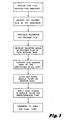
- FIG. 1 there is shown an eight step process of carrying out the invention and includes the provision of a thin film resistor ( TFR ) substrate which has been fabricated using state of the art semiconductor processing techniques.
- TFR thin film resistor
- a dry polymer film is then laminated on the upper surface of the TFR substrate, and this upper surface will typically be an inert barrier layer of either SiC or Si 3 N 4 .
- This polymer film is then partially polymerized with UV light and selectively developed to form an ink reservoir barrier mask on the TFR substrate. Then the barrier mask is subjected to additional ultraviolet light to provide a further cure thereof.
- a nozzle plate (also referred to sometimes as an orifice plate) is aligned with and placed upon the barrier mask in preparation for a heat stake operation described in more detail below with reference to Figure 3.
- the printhead structure is transferred to an oven for final curing at a predetermined time and elevated temperature.
- a thin film resistor structure which may be used in carrying out the present invention will typically consist of a silicon substrate member 10 upon which a thin silicon dioxide ,Si02, surface barrier layer 12 is deposited using known thermal oxidation techniques. Then, a resistive layer 14 of tantalum aluminum, TaAl, is sputtered deposited on top of the Si02 barrier layer 12, and thereafter a metalization pattern 16 which will typically be aluminum is formed as shown on the surface of the tantalum aluminum layer 14. The metalization pattern 16 will have openings therein defining the lateral dimensions of the individual resistors in the TFR structure.
- outer surface passivation layer 18 is deposited on the outer surface of the conductive pattern 16 and will typically consist of either silicon carbide, SiC, or silicon nitride, Si 3 N 4 . These latter materials are highly inert and are thus protective of the underlying materials from both ink corrosion and cavitation wear produced by the ink and ink ejections respectively during a thermal ink jet printing operation.
- the processing details used in producing a thin film resistor substrate structure of the type shown in Figure 2 are generally well known to those skilled in this art and more fully described in the above' identified Hewlett-Packard Journal published May 1985 and incorporated herein by reference.
- the TFR substrate of Figure 2 is illustrated only schematically as a single member in Figure 3A without showing the individual layers therein.
- Figures 3A - 3C still show the location of the four tantalum-aluminum heater resistors 20 which are subsequently aligned with the openings 22 in the polymer ink reservoir barrier layer 24.
- This barrier layer 24 is laminated on the TFR substrate 10 as a dry film of a material such as VACREL or RISTON which are trade names of photoresist polymer materials commercially available from the Dupont Company of Wilmington, Delaware.
- the polymer film 24 is processed using conventional photolithographic masking, ultraviolet exposure and etching techniques in order to form the plurality of openings 22 therein which define the boundaries of four individual ink reservoirs. These reservoirs are disposed immediately above the four resistive heater elements 20 of the thin film substrate 10 which supports it.
- the barrier layer 24 is developed to remove the unwanted selected portions of the dry film and create openings 22 therein, the structure of Figure 3A is exposed to some additional ultraviolet light to further UV cure the barrier layer 24 in accordance with the processing detail given below.
- an orifice or nozzle plate 26 having a plurality of openings 28 therein is aligned on the barrier layer 24 as shown, so that the orifices 28 are precisely centered with the ink reservoirs 22 in the barrier layer 24.
- a hot chuck 30 of a heat staker apparatus is moved down into thermal and pressure contact with the top surface of the nozzle plate 26 and held there at a predetermined pressure and for a predetermined time to partially thermally cure the barrier layer material 24. This step provides a good initial interface adherance and good surface contour match at the barrier layer-nozzle plate interface, as well as at the barrier
- the hot chuck 30 of the heat staker is brought into contact with the nozzle plate 28 under sufficient pressure to allow the barrier material 24 to plastically deform and adhere and conform to the contour of the upper surface of the nozzle plate 28. Then, the chuck 30 is released and the ink jet printhead of Figure 3C is transferred to a hot oven to fully cure the dry barrier film 24 in accordance with the processing schedule below.
- the present invention allows batch processing of parts during a nozzle plate attachment operation and thereby results in quick bonding of the nozzle plate 26 to the barrier layer 24 as indicated.
- This process deforms the dry film barrier layer 24 into the shape of the nozzle plate 28 to thereby fill any gaps therein, and in addition, further prevents the printhead substrate 10 from overheating during the nozzle plate attachment process.
- this process allows the batch processing of parts without the requirement for clamping, which has been a frequent requirement in prior dry film-adhesive cures.
- the present process eliminates the need for separate adhesives and adhesive bonding operations during the assembly process.
- the present process imparts long lasting structural integrity to the printhead structures being fabricated and insures permanent (plastic) deformation of the dry film barrier layer material.
- barrier layer materials are not limited to the particular VACREL and RISTON polymers sold by the Dupont Company and may instead employ other suitable polymer materials.
- the present invention is useful in the manufacture of thin film resistor type printheads used in thermal ink jet printers.
Landscapes
- Engineering & Computer Science (AREA)
- Manufacturing & Machinery (AREA)
- Particle Formation And Scattering Control In Inkjet Printers (AREA)
Applications Claiming Priority (2)
| Application Number | Priority Date | Filing Date | Title |
|---|---|---|---|
| US86119286A | 1986-05-08 | 1986-05-08 | |
| US861192 | 1986-05-08 |
Publications (2)
| Publication Number | Publication Date |
|---|---|
| EP0244643A2 true EP0244643A2 (fr) | 1987-11-11 |
| EP0244643A3 EP0244643A3 (fr) | 1988-09-28 |
Family
ID=25335136
Family Applications (1)
| Application Number | Title | Priority Date | Filing Date |
|---|---|---|---|
| EP87104971A Withdrawn EP0244643A3 (fr) | 1986-05-08 | 1987-04-03 | Procédé de fabrication de têtes d'impression pour imprimantes thermiques par jets d'encre |
Country Status (2)
| Country | Link |
|---|---|
| EP (1) | EP0244643A3 (fr) |
| JP (1) | JPS62264957A (fr) |
Cited By (4)
| Publication number | Priority date | Publication date | Assignee | Title |
|---|---|---|---|---|
| US6575560B2 (en) | 2000-07-10 | 2003-06-10 | Canon Kabushiki Kaisha | Liquid discharge recording head and liquid discharge recording apparatus |
| US6964467B2 (en) | 1999-12-22 | 2005-11-15 | Canon Kabushiki Kaisha | Liquid ejecting recording head and liquid ejecting recording apparatus |
| US7175255B2 (en) | 2003-10-23 | 2007-02-13 | Canon Kabushiki Kaisha | Ink jet recording head and ink jet recording apparatus |
| US7607761B2 (en) | 2005-12-27 | 2009-10-27 | Fuji Xerox Co., Ltd. | Droplet discharging head and manufacturing method for the same, and droplet discharging device |
Families Citing this family (8)
| Publication number | Priority date | Publication date | Assignee | Title |
|---|---|---|---|---|
| JP3343875B2 (ja) * | 1995-06-30 | 2002-11-11 | キヤノン株式会社 | インクジェットヘッドの製造方法 |
| KR20000001904A (ko) * | 1998-06-15 | 2000-01-15 | 윤종용 | 일체형 버블 잉크젯 프린터 헤드 및 그 제조방법 |
| JP4298066B2 (ja) | 1999-06-09 | 2009-07-15 | キヤノン株式会社 | インクジェット記録ヘッドの製造方法、インクジェット記録ヘッドおよびインクジェット記録装置 |
| ATE375865T1 (de) | 2001-08-10 | 2007-11-15 | Canon Kk | Verfahren zur herstellung eines flüssigkeitsausstosskopfes, substrat für einen flüssigkeitsausstosskopf und dazugehöriges herstellungsverfahren |
| JP2004001490A (ja) | 2002-04-23 | 2004-01-08 | Canon Inc | インクジェットヘッド |
| JP2004001488A (ja) | 2002-04-23 | 2004-01-08 | Canon Inc | インクジェットヘッド |
| JP3950730B2 (ja) | 2002-04-23 | 2007-08-01 | キヤノン株式会社 | インクジェット記録ヘッドおよびインク吐出方法 |
| JP5188049B2 (ja) | 2006-09-13 | 2013-04-24 | キヤノン株式会社 | 記録ヘッド |
Family Cites Families (6)
| Publication number | Priority date | Publication date | Assignee | Title |
|---|---|---|---|---|
| JPS5961940A (ja) * | 1982-09-30 | 1984-04-09 | Sharp Corp | 半導体チツプのボンデイング方法 |
| JPH0624855B2 (ja) * | 1983-04-20 | 1994-04-06 | キヤノン株式会社 | 液体噴射記録ヘッド |
| EP0124312A3 (fr) * | 1983-04-29 | 1985-08-28 | Hewlett-Packard Company | Structures de résistance pour imprimantes à jet d'encre thermiques |
| US4535343A (en) * | 1983-10-31 | 1985-08-13 | Hewlett-Packard Company | Thermal ink jet printhead with self-passivating elements |
| JPS60203451A (ja) * | 1984-03-28 | 1985-10-15 | Canon Inc | インクジエツト記録ヘツド |
| JPS61252164A (ja) * | 1985-05-01 | 1986-11-10 | Alps Electric Co Ltd | インクジエツトヘツド |
-
1987
- 1987-04-03 EP EP87104971A patent/EP0244643A3/fr not_active Withdrawn
- 1987-05-08 JP JP11222187A patent/JPS62264957A/ja active Pending
Cited By (7)
| Publication number | Priority date | Publication date | Assignee | Title |
|---|---|---|---|---|
| US6964467B2 (en) | 1999-12-22 | 2005-11-15 | Canon Kabushiki Kaisha | Liquid ejecting recording head and liquid ejecting recording apparatus |
| US7118193B2 (en) | 1999-12-22 | 2006-10-10 | Canon Kabushiki Kaisha | Liquid ejecting recording head and liquid ejecting recording apparatus |
| US6575560B2 (en) | 2000-07-10 | 2003-06-10 | Canon Kabushiki Kaisha | Liquid discharge recording head and liquid discharge recording apparatus |
| US7175255B2 (en) | 2003-10-23 | 2007-02-13 | Canon Kabushiki Kaisha | Ink jet recording head and ink jet recording apparatus |
| US7296869B2 (en) | 2003-10-23 | 2007-11-20 | Canon Kabushiki Kaisha | Ink jet recording head and ink jet recording apparatus |
| US7607761B2 (en) | 2005-12-27 | 2009-10-27 | Fuji Xerox Co., Ltd. | Droplet discharging head and manufacturing method for the same, and droplet discharging device |
| US8141250B2 (en) | 2005-12-27 | 2012-03-27 | Fuji Xerox Co., Ltd. | Method of manufacturing a droplet discharging head |
Also Published As
| Publication number | Publication date |
|---|---|
| JPS62264957A (ja) | 1987-11-17 |
| EP0244643A3 (fr) | 1988-09-28 |
Similar Documents
| Publication | Publication Date | Title |
|---|---|---|
| US6409312B1 (en) | Ink jet printer nozzle plate and process therefor | |
| US5686224A (en) | Ink jet print head having channel structures integrally formed therein | |
| EP0244643A2 (fr) | Procédé de fabrication de têtes d'impression pour imprimantes thermiques par jets d'encre | |
| EP0609860A2 (fr) | Méthode pour la fabrication d'une tête à jet d'encre | |
| JPH10291319A (ja) | ノズル・プレートを個々に分離して印刷ヘッドに取り付ける方法 | |
| JP2008087478A (ja) | インクジェットプリントヘッド及びその製造方法 | |
| EP1559554B1 (fr) | Procédé de fabrication d'une tête d'impression à jet d'encre | |
| US4570167A (en) | Ink jet recording head | |
| JPS58224760A (ja) | インクジエツト記録ヘツド | |
| US6852241B2 (en) | Method for making ink jet printheads | |
| JP2009143228A (ja) | インクジェット印刷ヘッド及びその製造方法 | |
| JP2000255072A (ja) | インクジェット記録ヘッドの製造方法およびインクジェット記録ヘッド | |
| JP3231544B2 (ja) | インクジェットヘッドの製造方法 | |
| KR20100029635A (ko) | 잉크젯 프린트헤드 및 그 제조방법 | |
| JP3652022B2 (ja) | インクジェット記録ヘッド及びインクジェット記録ヘッドの製造方法 | |
| KR100468161B1 (ko) | 모노리식 잉크젯 프린트 헤드의 제조방법 | |
| KR100856412B1 (ko) | 잉크젯 프린트헤드의 제조방법 | |
| JPH0242670B2 (fr) | ||
| JPH08142327A (ja) | インクジェット記録装置の記録ヘッド | |
| JP2002160369A (ja) | インクジェット記録ヘッドおよびその製造方法 | |
| JPH07164639A (ja) | インクジェット記録ヘッド、その製造方法、およびその記録ヘッドを備えた記録装置 | |
| JPH07156414A (ja) | インクジェット記録ヘッドの製造方法、インクジェット記録ヘッド、および記録装置 | |
| JP2001191540A (ja) | ノズル形成部材及びその製造方法、インクジェットヘッド並びにインクジェット記録装置 | |
| JPH0631920A (ja) | インクジェット記録ヘッド及びその製造方法 | |
| US20070091147A1 (en) | Liquid discharge head and method of producing the same |
Legal Events
| Date | Code | Title | Description |
|---|---|---|---|
| PUAI | Public reference made under article 153(3) epc to a published international application that has entered the european phase |
Free format text: ORIGINAL CODE: 0009012 |
|
| AK | Designated contracting states |
Kind code of ref document: A2 Designated state(s): DE FR GB IT |
|
| PUAL | Search report despatched |
Free format text: ORIGINAL CODE: 0009013 |
|
| AK | Designated contracting states |
Kind code of ref document: A3 Designated state(s): DE FR GB IT |
|
| STAA | Information on the status of an ep patent application or granted ep patent |
Free format text: STATUS: THE APPLICATION IS DEEMED TO BE WITHDRAWN |
|
| 18D | Application deemed to be withdrawn |
Effective date: 19890329 |
|
| RIN1 | Information on inventor provided before grant (corrected) |
Inventor name: BERRETTA, FREDERICK S. Inventor name: BEARSS, JAMES G. Inventor name: NIGRO, STEPHEN J. Inventor name: MEYER, WESLEY L. |