EP0244655B1 - Festkörper-Farbbildaufnahmegerät - Google Patents
Festkörper-Farbbildaufnahmegerät Download PDFInfo
- Publication number
- EP0244655B1 EP0244655B1 EP87105138A EP87105138A EP0244655B1 EP 0244655 B1 EP0244655 B1 EP 0244655B1 EP 87105138 A EP87105138 A EP 87105138A EP 87105138 A EP87105138 A EP 87105138A EP 0244655 B1 EP0244655 B1 EP 0244655B1
- Authority
- EP
- European Patent Office
- Prior art keywords
- transfer
- color
- photosensitive
- signal charges
- pickup apparatus
- Prior art date
- Legal status (The legal status is an assumption and is not a legal conclusion. Google has not performed a legal analysis and makes no representation as to the accuracy of the status listed.)
- Expired - Lifetime
Links
- 239000007787 solid Substances 0.000 title claims description 77
- 238000003860 storage Methods 0.000 claims description 140
- 238000006243 chemical reaction Methods 0.000 claims description 111
- 239000003086 colorant Substances 0.000 claims description 48
- 230000000295 complement effect Effects 0.000 claims description 12
- 239000000463 material Substances 0.000 claims description 6
- 238000005036 potential barrier Methods 0.000 claims description 6
- 229910052782 aluminium Inorganic materials 0.000 claims description 5
- XAGFODPZIPBFFR-UHFFFAOYSA-N aluminium Chemical compound [Al] XAGFODPZIPBFFR-UHFFFAOYSA-N 0.000 claims description 5
- 229920006395 saturated elastomer Polymers 0.000 claims description 3
- 230000006798 recombination Effects 0.000 claims 1
- 238000005215 recombination Methods 0.000 claims 1
- 230000035945 sensitivity Effects 0.000 description 21
- 238000000034 method Methods 0.000 description 18
- 238000001444 catalytic combustion detection Methods 0.000 description 14
- 230000006870 function Effects 0.000 description 13
- 238000007639 printing Methods 0.000 description 11
- 239000000758 substrate Substances 0.000 description 8
- 238000010276 construction Methods 0.000 description 7
- 239000011159 matrix material Substances 0.000 description 7
- 229910021420 polycrystalline silicon Inorganic materials 0.000 description 7
- 229920005591 polysilicon Polymers 0.000 description 7
- 230000008569 process Effects 0.000 description 7
- 230000004888 barrier function Effects 0.000 description 5
- 238000010586 diagram Methods 0.000 description 5
- 230000003287 optical effect Effects 0.000 description 5
- 238000002360 preparation method Methods 0.000 description 5
- 229920001296 polysiloxane Polymers 0.000 description 4
- 230000001360 synchronised effect Effects 0.000 description 4
- 239000004642 Polyimide Substances 0.000 description 3
- 230000006872 improvement Effects 0.000 description 3
- 229920001721 polyimide Polymers 0.000 description 3
- XUIMIQQOPSSXEZ-UHFFFAOYSA-N Silicon Chemical compound [Si] XUIMIQQOPSSXEZ-UHFFFAOYSA-N 0.000 description 2
- GWEVSGVZZGPLCZ-UHFFFAOYSA-N Titan oxide Chemical compound O=[Ti]=O GWEVSGVZZGPLCZ-UHFFFAOYSA-N 0.000 description 2
- TZCXTZWJZNENPQ-UHFFFAOYSA-L barium sulfate Chemical compound [Ba+2].[O-]S([O-])(=O)=O TZCXTZWJZNENPQ-UHFFFAOYSA-L 0.000 description 2
- 230000015572 biosynthetic process Effects 0.000 description 2
- 230000000694 effects Effects 0.000 description 2
- 238000000819 phase cycle Methods 0.000 description 2
- 230000002441 reversible effect Effects 0.000 description 2
- 229910052710 silicon Inorganic materials 0.000 description 2
- 239000010703 silicon Substances 0.000 description 2
- 230000003068 static effect Effects 0.000 description 2
- VYZAMTAEIAYCRO-UHFFFAOYSA-N Chromium Chemical compound [Cr] VYZAMTAEIAYCRO-UHFFFAOYSA-N 0.000 description 1
- 230000010748 Photoabsorption Effects 0.000 description 1
- VYPSYNLAJGMNEJ-UHFFFAOYSA-N Silicium dioxide Chemical compound O=[Si]=O VYPSYNLAJGMNEJ-UHFFFAOYSA-N 0.000 description 1
- 238000009825 accumulation Methods 0.000 description 1
- PNEYBMLMFCGWSK-UHFFFAOYSA-N aluminium oxide Inorganic materials [O-2].[O-2].[O-2].[Al+3].[Al+3] PNEYBMLMFCGWSK-UHFFFAOYSA-N 0.000 description 1
- 230000005540 biological transmission Effects 0.000 description 1
- 238000010351 charge transfer process Methods 0.000 description 1
- 230000006835 compression Effects 0.000 description 1
- 238000007906 compression Methods 0.000 description 1
- 238000007796 conventional method Methods 0.000 description 1
- 229910052593 corundum Inorganic materials 0.000 description 1
- 230000003247 decreasing effect Effects 0.000 description 1
- 230000000593 degrading effect Effects 0.000 description 1
- 230000003111 delayed effect Effects 0.000 description 1
- 230000001419 dependent effect Effects 0.000 description 1
- 230000006866 deterioration Effects 0.000 description 1
- 229910003460 diamond Inorganic materials 0.000 description 1
- 239000010432 diamond Substances 0.000 description 1
- 238000007599 discharging Methods 0.000 description 1
- 238000005516 engineering process Methods 0.000 description 1
- 238000002347 injection Methods 0.000 description 1
- 239000007924 injection Substances 0.000 description 1
- 230000010354 integration Effects 0.000 description 1
- 150000002500 ions Chemical class 0.000 description 1
- -1 lithopone Substances 0.000 description 1
- CPLXHLVBOLITMK-UHFFFAOYSA-N magnesium oxide Inorganic materials [Mg]=O CPLXHLVBOLITMK-UHFFFAOYSA-N 0.000 description 1
- 238000004519 manufacturing process Methods 0.000 description 1
- 229910052751 metal Inorganic materials 0.000 description 1
- 239000002184 metal Substances 0.000 description 1
- 239000010445 mica Substances 0.000 description 1
- 229910052618 mica group Inorganic materials 0.000 description 1
- 239000000203 mixture Substances 0.000 description 1
- 230000036961 partial effect Effects 0.000 description 1
- 239000000049 pigment Substances 0.000 description 1
- 239000002985 plastic film Substances 0.000 description 1
- 239000004800 polyvinyl chloride Substances 0.000 description 1
- 229920000915 polyvinyl chloride Polymers 0.000 description 1
- 238000012805 post-processing Methods 0.000 description 1
- 230000002265 prevention Effects 0.000 description 1
- 230000003449 preventive effect Effects 0.000 description 1
- 230000009467 reduction Effects 0.000 description 1
- 230000002829 reductive effect Effects 0.000 description 1
- 230000008929 regeneration Effects 0.000 description 1
- 238000011069 regeneration method Methods 0.000 description 1
- 239000004065 semiconductor Substances 0.000 description 1
- 238000000926 separation method Methods 0.000 description 1
- GGCZERPQGJTIQP-UHFFFAOYSA-N sodium;9,10-dioxoanthracene-2-sulfonic acid Chemical compound [Na+].C1=CC=C2C(=O)C3=CC(S(=O)(=O)O)=CC=C3C(=O)C2=C1 GGCZERPQGJTIQP-UHFFFAOYSA-N 0.000 description 1
- 239000004408 titanium dioxide Substances 0.000 description 1
- 229910001845 yogo sapphire Inorganic materials 0.000 description 1
- XLOMVQKBTHCTTD-UHFFFAOYSA-N zinc oxide Inorganic materials [Zn]=O XLOMVQKBTHCTTD-UHFFFAOYSA-N 0.000 description 1
Images










Classifications
-
- H—ELECTRICITY
- H04—ELECTRIC COMMUNICATION TECHNIQUE
- H04N—PICTORIAL COMMUNICATION, e.g. TELEVISION
- H04N1/00—Scanning, transmission or reproduction of documents or the like, e.g. facsimile transmission; Details thereof
- H04N1/46—Colour picture communication systems
- H04N1/48—Picture signal generators
- H04N1/486—Picture signal generators with separate detectors, each detector being used for one specific colour component
-
- H—ELECTRICITY
- H04—ELECTRIC COMMUNICATION TECHNIQUE
- H04N—PICTORIAL COMMUNICATION, e.g. TELEVISION
- H04N1/00—Scanning, transmission or reproduction of documents or the like, e.g. facsimile transmission; Details thereof
- H04N1/46—Colour picture communication systems
- H04N1/64—Systems for the transmission or the storage of the colour picture signal; Details therefor, e.g. coding or decoding means therefor
- H04N1/646—Transmitting or storing colour television type signals, e.g. PAL, Lab; Their conversion into additive or subtractive colour signals or vice versa therefor
-
- H—ELECTRICITY
- H04—ELECTRIC COMMUNICATION TECHNIQUE
- H04N—PICTORIAL COMMUNICATION, e.g. TELEVISION
- H04N25/00—Circuitry of solid-state image sensors [SSIS]; Control thereof
- H04N25/10—Circuitry of solid-state image sensors [SSIS]; Control thereof for transforming different wavelengths into image signals
- H04N25/11—Arrangement of colour filter arrays [CFA]; Filter mosaics
- H04N25/13—Arrangement of colour filter arrays [CFA]; Filter mosaics characterised by the spectral characteristics of the filter elements
- H04N25/135—Arrangement of colour filter arrays [CFA]; Filter mosaics characterised by the spectral characteristics of the filter elements based on four or more different wavelength filter elements
- H04N25/136—Arrangement of colour filter arrays [CFA]; Filter mosaics characterised by the spectral characteristics of the filter elements based on four or more different wavelength filter elements using complementary colours
Definitions
- the invention relates to a solid state image pickup apparatus comprising a plurality of photodetectors which are arranged in horizontal and verticle rows and are illuminated to provide signal charges which are read to provide an image signal.
- a solid state image pickup device in which signal charges obtained by a plurality of photodetectors arranged in horizontal and verticle rows are read by a verticle transfer unit extending along a verticle row of the photodetectors, are transferred at high speed from the transfer unit to a storage unit, and are transferred for each of one or more horizontal photodetectors from the storage unit to a horizontal transfer unit. The signal charges are further transferred by the horizontal transfer unit to an output unit.
- CCD type color solid state imager in which color signals respectively separated in time can be derived from picture elements for respective colors arrayed in the shape of a matrix and which permits interlacing without degrading a resolution and without causing image lag.
- Pairs of CCD shift registers which are electrically insulated and separated and which run in the verticle direction are arrayed in the horizontal direction, signal charges stored in adjacent picture elements are sent to the individual opposing CCD registers through transfer gates arrayed in a checkerboard pattern, and signal charges transferred in time sequence are distributed to a plurality of CCD shift registers which run in the horizontal direction.
- the former is composed of a photosensitive portion 1 and a charge storage portion 2 provided separately from the photosensitive portion 1.
- the photosensitive portion 1 there are horizontally arranged a plurality of photosensitive blocks a1-a n formed with self-scanning type pickup elements performing photosensitive storage and transfer operation, each of the photosensitive blocks a1-a n being covered with a striped color filter.
- the charge storage portion 2 comprises CCD shift registers b1-b n formed adjacently to the photosensitive blocks a1-a n and covered with an aluminum film or the like for shading.
- a read shift register 3 formed of a horizontal CCD shift register is connected to the one end of each of the CCD shift registers b1-b n .
- the signal charge generated in the photosensitive portion 1 is controlled by a predetermined transfer drive signal and transferred to the charge storage portion 2.
- the signal charges equivalent to one image derived from the photosensitive portion 1 are temporarily stored in the charge storage portion 2 and the signal charges equivalent to one line are sequentially outputted through the read shift register 3 to an output terminal 4.
- each light receiving element 5 being composed of a photodiode and so on whose surface is covered with a given color filter.
- the signal charge generated in each light receiving element 5 is transferred to a transfer shift register 7 through a transfer gate 6 and then the signal charges equivalent to one line are sequentially transferred to a read shift register 8 by the transfer shift register 7.
- the signal charges thus transferred are sequentially outputted through a read shift register 8 comprising a horizontal CCD shift register, whereby the signal charges equivalent to one image are outputted to an output terminal 9.
- each transfer shift register 7 is shaded by an aluminum film to prevent any noise component derived from external light from mixing with the signal charge.
- the photosensitive portion 1 functions as an accumulator for accumulating the signals resulting from photoelectric conversion and a transferer for transferring the mass of the signal charge thus accumulated to the charge storage portion 2.
- the effective accumulating time required for the accumulation of the signal charge cannot be increased and therefore it is difficult to improve the sensitivity.
- the photosensitive portion is covered with polysilicon for use as a transfer electrode, ⁇ short wavelength light is particularly prevented from passing therethrough and thereby the sensitivity is restricted.
- the presence of the shaded transfer shift register in the light receiving means also makes it difficult to improve light storage efficiency and further the shaded portion causes horizontal resolution to reduce.
- the present invention is intended to solve the aforesaid problems and it is therefore an object of the invention to provide a solid pickup apparatus offering improved sensitivity and resolution.
- Figs. 1 and 2 represent a schematic structural view of a conventional solid pickup apparatus.
- Fig. 3 represents a schematic structural view of a first solid state image pickup apparatus embodying the present invention.
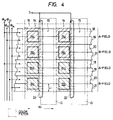
- Fig. 4 shows the structure of the principal part of the surface of the photosensitive zone of Fig. 3.
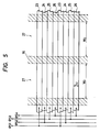
- Fig. 5 shows the structure of the principal part of the surface of the charge storage zone of Fig. 3.
- Fig. 6 represents a schematic structural view of a second solid state image pickup apparatus embodying the present invention.
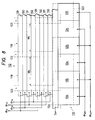
- Figs. 7 and 8 show in detail the principal part of the surface of the construction of Fig. 6.
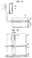
- Fig. 9 shows a schematic arrangement where the solid state image pickup apparatus embodying the present invention is applied to printing equipment.
- Fig. 10 represents a schematic structural view of a third solid state image pickup apparatus intended to describe its structure and operation.
- Fig. 11 represent a schematic structural view of a fourth solid state image pickup apparatus intended to describe its structure and operation.
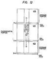
- Fig. 12 represents a schematic structural view of a fifth solid state image pickup apparatus intended to describe its structure and operation.
- Fig. 13 represents an enlarge view illustrating the first light receiving zone of Fig. 1.
- Fig. 14 is a structural view illustrating a sixth embodiment of the present invention.
- Fig. 15 is a structural view illustrating a seventh embodiment of the present invention.
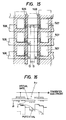
- Fig. 16 is a diagram illustrating a conventional virtual phase CCD.
- Fig. 17 is a top view of an element as an eighth embodiment of the present invention.
- Fig. 18 is a sectional view of the element of Fig. 17.
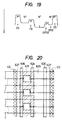
- Fig. 19 is a potential profile.
- Fig. 20 is a top view of another embodiment of the present invention.
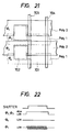
- Fig. 21 is a top view of a solid pickup element to which a ninth embodiment of the present invention applies.
- Fig. 22 is a diagram illustrating voltage applied to a transfer electrode in the storage mode.
- Fig. 23 is a structural view of a solid pickup apparatus illustrating a tenth embodiment of the present invention.
- Fig. 24 is a graph showing photosensitive characteristics of vertical transfer lines and photodiodes of a solid state image pickup apparatus employing the vertical transfer line as a photoelectric conversion means.
- Fig. 25 is a schematic diagram relating to reading and recording method.
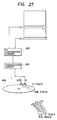
- Figs. 26 and 27 are diagrams illustrating the progress of process.
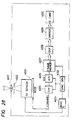
- Fig. 28 is a block diagram of an electronic still image camera with a solid state image pickup apparatus according to the present invention.
- Fig. 3 is a schematic structural view of a solid state image pickup apparatus of a first embodiment of the present invention, wherein the apparatus comprises a photosensitive portion 10, a charge storage portion 11, a first horizontal charge transfer means 12 and a second horizontal charge transfer means 13, each of the last two means being shown simply in the form of a block.
- the photosensitive portion 10 shown in Fig. 3 is composed of photosensitive blocks 14, each consisting of a group of light receiving elements which are photoelectric conversion elements such as photodiodes arranged vertically as shown by a square dotted line and photosensitive (vertical) transfer blocks 15, each of which is arranged side by side with each group.
- a plurality of photosensitive blocks 14 and that of photosensitive transfer blocks 15 are arranged alternately in the horizontal direction (left to right in Fig.3).
- the pairs of light receiving elements are covered alternately with red filters Ra, Rb and blue filters Ba, Bb wherein the vertical direction means a direction perpendicular to the aforesaid horizontal direction in the photosensitive block 14.
- the photosensitive transfer block 15 shown by the square dotted line of Fig. 3 is composed of photosensitive transfer elements arranged vertically so that each of them is adapted to correspond to each light receiving element.
- Each photosensitive transfer element is a CCD (Charge Coupled Device) exercising a photoelectric effect and functioning as a transferer for transferring the signal charge to the charge storage portion 11 through mutual signal transfer operation. That is, the photosensitive transfer block 15 is composed of self-scanning type pickup devices functioning as a photosensitive storage device and a transfer device.
- CCD Charge Coupled Device
- the surface of the photosensitive transfer block 15 is covered with a striped green filter G.
- CCD shift registers equivalent in number to the photosensitive transfer blocks 15, so that the signal charge from a particular transfer block 15 is stored in a particular CCD shift register.
- a first horizontal charge transfer means 12 which is a horizontal CCD shift register for horizontally transferring the signal charge and both sides of the first horizontal charge transfer means 12 are connected with the photosensitive portion 10 and the charge storage portion 11 through transfer gates Tg1, Tg2, respectively.
- the other end of the charge storage portion 11 is connected with the side of a second horizontal charge transfer means 13 through a transfer gate Tg3, the second horizontal charge transfer means 13 being formed with a horizontal CCD shift register for horizontally transferring the signal charge.
- the block enclosed by a dotted line is a channel stopper 16 formed on a silicon substrate and the light receiving elements of the photosensitive block 14 are formed in the portion enclosed by the channel stopper 16.
- the light receiving elements are covered alternately with the red filters Ra, Rb and blue filters Ba, Bb.
- the photosensitive transfer block 15 enclosed by the channel stopper 16and covered with the green filter G is formed between the photosensitive blocks 14.
- transfer electrodes 18, 19, 20, 21 of polysilicon layers horizontally extended are alternately formed in the vertical direction and the channel portions located in the lower portions of the transfer electrodes 18, 19, 20, 21 conform to the aforesaid photosensitive transfer elements.
- the portion corresponding to the horizontal direction of the transfer electrodes 18, 19 is called a field A
- the portion corresponding to the horizontal direction of the transfer electrodes 20, 21 is called a field B, whereby interlace scanning for use in television as will be described later can be implemented.
- the relation of the light receiving element of the photosensitive block 14 to the color filter is such that one pitch of the color filter is assigned to a pair of the two light receiving elements in the vertical direction, whereas one pitch of the filter is assigned to each of one light receiving element and one photosensitive transfer element of the photosensitive transfer block 15 in the horizontal direction.
- the elements covered with the filters Ra, Ba of the red and blue filters, and the green filters G corresponding to the filters Ra, Ba are caused to deal with the field A
- the elements covered with the filters Ra, Rb of the red and blue filters, and the green filters G corresponding to the filters Ra, Ba are caused to deal with the field B.
- a transfer gate 22 for controlling the transfer of the signal charge generated in each light receiving element to the photosensitive transfer block 15 is installed in a part of the channel stopper 16 for separating the photosensitive block 14 from the photosensitive transfer block 15.
- the polysilicon layers forming the transfer electrodes 18, 19, 20, 21 are overlapped so as to prevent their mutually disjunctive portions from conducting and are also provided with a recess in order not to cover the light receiving elements of the photosensitive block 14.
- Fig. 5 shows a part of the structure of the charge storage portion, wherein the portion indicated by dotted and slant lines represents the channel stopper 16 and wherein parallel transfer electrodes 23, 24, 25, 26 of polysilicon layers are vertically formed on the surface of the layer between the channel stoppers 16 to provide CCD shift registers 27.
- the width W2 in the horizontal direction of the channel portion constituted by the transfer electrodes 23, 24, 25, 26 is set roughly equal to the width W1 in the horizontal direction of a pair of a photosensitive block 14 and a photosensitive transfer block 15, whereas the channel length L2 of each of the transfer electrodes 23, 24, 25, 26 of the charge storage portion 11 is set shorter than the channel length L1 of each of the transfer electrodes 18, 19, 20, 21 of the photosensitive portion 10.
- the channel length L2 is determined correspondingly to the quantity of signal charge transferred from the photosensitive transfer block 15. For example, in a case where L2 is set half of channel L1, the area occupied by the charge storage portion 11 can be made roughly half the area of the photosensitive portion 10.
- each of the CCD shift registers 27 is subordinately connected to each pair of a photosensitive block 14 and a photosensitive transfer block 15. Accordingly, it becomes possible to make the vertical width of the charge storage portion 11 narrower than that of the photosensitive portion 10.
- the first horizontal charge transfer means 12 shown in Fig. 3 is formed between the photosensitive portion 10 and the charge storage portion 11 shown in Fig. 4, 5.
- the transfer gates Tg1, Tg2 By applying predetermined gate voltage to the transfer gates Tg1, Tg2 and causing them to perform ON operation, the signal charge of the photosensitive portion 10 is transferred to the charge storage portion 11 through the first horizontal charge transfer means 12.
- the channel portions equal in number to the photosensitive transfer blocks 15 for electrically connecting the photosensitive transfer blocks 15 to the CCD shift registers 27 corresponding thereto. Accordingly, the signal charges can be transferred from the photosensitive portion 10 to the charge storage portion 11 by turning on both of the transfer gates Tg1, Tg2, while by holding the transfer gates Tg1, Tg2 off and causing the first horizontal charge transfer means 12 to perform shift operation, the signal charges can be outputted from the output terminal 29.
- the channel portions equal in number to the CCD shift registers 27 of the charge storage portion 11 are horizontally formed and, by turning on the transfer gate Tg3, the signal charges from the charge storage portion 11 are received, whereby the signals are sequentially outputted from the output terminal 30 through the horizontal shift operation.
- the transfer gates Tg1, Tg2 are turned on and four-phase clock driven pulse signals ⁇ V1, ⁇ V2, ⁇ V3, ⁇ V4 are applied to the transfer electrodes 18, 19, 20, 21 to transfer the green color signal charges of the photosensitive transfer blocks 14 to the charge storage portion 11.
- the synchronous pulse signals ⁇ V1, ⁇ V2, ⁇ V3, ⁇ V4 are applied to the transfer electrodes 23, 24, 25, 26 of the charge storage portion 11, the green color signal charges as they are originally arranged in the photosensitive transfer blocks 15 are transferred to the charge storage portion 11.
- the transfer gates Tg1, Tg2, Tg3 are turned off and closed, whereas the transfer gate 22 is turned on and opened. Then the red and blue color signal charges of the light receiving elements of the photosensitive blocks 14 are transferred to the photosensitive transfer elements of the photosensitive transfer blocks 15.
- color signal charges equivalent to one line are transferred to the first and second horizontal transfer means 12, 13 again and the repetition of the control operation allows image signals equivalent to one image generated in the photosensitive portion 10 to be outputted.
- the shutter exposure is further repeated to obtain image signals equivalent to the next one image.
- the control of the drive signals and the transfer gates is implemented by a drive control circuit and electric signals corresponding to the interline arrangement are available to both the fields A, B.
- totally two horizontal charge transfer means are provided between the photosensitive portion and the charge storage portion and on the side of the charge storage portion, respectively, to separate the color signals R/B and G and output.
- Fig. 6 is a schematic structural view of a solid state image pickup apparatus, as a second embodiment of the present invention, manufactured through circuit integration technology, wherein the apparatus comprises a photosensitive portion 110, a charge storage portion 111, a transfer gate 112, a horizontal shift register 113, a buffer amplifier 114, a switching circuit 115 and a drive control circuit 116 simply shown in the form of an individual block.
- Fig. 7, 8 show the detailed principal portions of the surfaces indicative of the structure of the apparatus of Fig. 6.
- Fig. 7 shows the connecting portion between the photosensitive portion 110 and the charge storage portion 111; and
- Fig. 8 shows the connecting portions between the charge storage portion 111 and the transfer gate 112 and between the charge storage portion 111 and the horizontal shift register 113.
- the horizontal CCD shift register 113 is formed at the end of the charge storage portion 111 through the transfer gate 112 and the output means of the horizontal CCD shift register 113 is connected to the switching circuit 115 through the buffer amplifier 114.
- the switching circuit 115 has gate elements 120, 121 such as transmission gates whose one node commonly is connected to the output terminal of the buffer amplifier 114 and the other is separately connected to output terminals Q1, Q2, both the gate elements 120, 121 being mutually exclusively turned on and off by an inverter 122 connected therebetween.
- the drive control circuit 116 produces, e.g., four-phase drive signals ⁇ v1- ⁇ v4, ⁇ s1- ⁇ s4 applied to the photosensitive portion 10 and the charge storage portion 111; a control signal S1 for controlling the on/off operation of the transfer gate 112; two-phase drive signals ⁇ h1, ⁇ h2 for controlling the shift operation of the horizontal shift register 113; and a switch control signal S2 for controlling the switching of the switching circuit 115.
- a channel stopper 123 formed on a silicon substrate and in the portion enclosed by the channel stopper 123 are light receiving elements 117a of a photosensitive block 117 and a photosensitive transfer block 118, i.e., a self-scanning type CCD shift register, or described in the first embodiment.
- red and blue color filters Ra, Rb, Ba,Bb so arranged as shown in Fig. 6 are installed in the photosensitive block 117, whereas the photosensitive transfer block 118 is covered with a striped green filter G.
- the width W2 in the horizontal direction of the channel constituted by the transfer electrodes 124-127 is roughly set equal to that between a pair of photosensitive block 117 and photosensitive transfer block 118 in the horizontal direction.
- the length L2 of each channel constituted by the transfer electrodes 124-127 of the photosensitive transfer block 118 is set shorter than the channel length L1 of each of the transfer electrodes 124-127 of the photosensitive transfer block 118.
- the length L2 is set about half each channel length L1 in this embodiment.
- the setting value is made to correspond to the quantity of signal charge being transferred from the photosensitive transfer block 118, so that the area occupied by the charge storage portion 11 can effectively be set smaller than the area of the photosensitive portion 110.
- L2 is set half of channel L1
- the area occupied by the charge storage portion 111 can be made roughly half the area of the photosensitive portion 110.
- the horizontal shift register 113 is formed on the output side of the charge storage portion 111 through the transfer gate 112.
- Polysilicon wiring 133 provided in parallel to the transfer electrode 132 installed at the end of the charge storage portion 111 forms the on/off channel of the transfer gate 112 and, under the control of the control signal S1, controls the on/off state of the transfer of the signal charge from the vertical CCD shift register 119 to the horizontal shift register 113.
- CCD shift registers constitute the horizontal shift register and, by applying predetermined drive signals, e.g., two-phase drive signals ⁇ h1, ⁇ h2 to horizontally-arranged transfer electrodes 134, 135, the signal charges equivalent to one line, which are transferred from the charge storage portion 110 are sequentially transferred to the buffer amplifier 114.
- predetermined drive signals e.g., two-phase drive signals ⁇ h1, ⁇ h2
- transfer electrodes 134, 135 horizontally-arranged transfer electrodes 134, 135
- Fig. 9 is a schematic structural view of the aforesaid system, wherein a solid state image pickup apparatus 136 is installed in the following stage of an electronic color camera as an optical system.
- the output terminals Q1, Q2 of the apparatus 136 are respectively connected to the printing heads 138, 139 of a printer 137 so that the output of the former is supplied to the red and blue color printing head 138 and that the output of the latter is supplied to the green color recording head 139.
- Printing paper 140 (not shown) supplied onto the platen of the printer 137 is printed with color images.
- An optical image of an object is first formed on the photosensitive portion 110 through the shutter exposure of the electronic camera and red and blue color signal charges are produced in the light receiving elements 117a of the photosensitive blocks 117, whereas green color signal charges are generated in the photosensitive transfer elements of the photosensitive transfer blocks 118.
- the shutter is closed a predetermined time later and drive signals ⁇ v1- ⁇ v4, ⁇ s1- ⁇ s4 are respectively supplied by a drive control circuit to the transfer electrodes 124-127, 129-132 of the photosensitive portion 110 and the charge storage portion 111 to transfer the green color signal charges to the charge storage portion 111.
- the supply of the drive signals ⁇ v1- ⁇ v4, ⁇ s1- ⁇ s4 is stopped and, after a control signal S1 is supplied to the transfer gate 112 to open the channels, the drive signals ⁇ s1- ⁇ s4 are supplied to transfer signal charges amounting to one line from the charge storage portion 111 to the horizontal shift register 113.
- drive signals ⁇ h1, ⁇ h2 are supplied to the horizontal shift register 113 to transfer the green color signal charges to the buffer amplifier 114.
- gate elements 120, 121 are so arranged as to be respectively turned on and off by a control signal S2 produced by the drive control circuit. Consequently, as shown in Fig. 9, green color signals are supplied from the output terminal Q2 to the green color recording head 139 and green color picture element data equivalent to one horizontal scanning is printed on the paper.
- a control signal TI is supplied from the drive control circuit to a transfer gate 125 (Fig. 7) to open the channels and cause the red and blue color signal charges stored in the photosensitive blocks 117 to transfer to the photosensitive transfer blocks 118. Subsequently after the transfer gate 125 is closed again, all the red and blue color signal charges are transferred to the charge storage portion 111 in the same control of the transfer operation from the color signal charges corresponding to green color to the charge storage portion 111.
- the gate elements 121, 120 of the switching circuit 115 are respectively opened and closed by the control signal S2 and, as in the case of the transfer of the aforesaid recording color signal charges, the signal charge transfer operation on a horizontal scanning basis is repeated by the charge storage portion 111, the transfer gate 112 and the horizontal shift register 113 and the repetition of one horizontal scanning is synchronously carried out by the red and blue printing head 138 shown in Fig. 9, so that red and blue data is printed on the paper.
- Exposure and the transfer of signal charges by means of the solid pickup apparatus is synchronized with the printing operation of the color printer 137, whereby color printing using an electronic camera can be facilitated.
- the signals for use are not limited to four-phase.
- two-phase signals are also usable.
- the color filter arrangement and the number of horizontal transfer means are not limited to those described in the aforesaid embodiment.
- one (G) of the three primary colors or a complementary color has been arranged in the form of stripes on each filter for the photosensitive (vertical) transfer block and the two remaining colors(R,B) have been arranged in the form of a mosaic.
- a third embodiment of the present invention shown in Fig. 10 three kinds of filters are vertically extended in the form of stripes and, of the three kinds of colors, two of them are used for filters in the photosensitive (vertical) transfer block and the last one is employed for filters in the photosensitive block.
- a light receiving portion 201 is provided with photoelectric conversion elements arranged in the form of a matrix and the light receiving zone 201 is covered with a microcolor filter.
- the microcolor filter bears three colors R, G, B corresponding to each photoelectric conversion element.
- the microcolor filter according to the present invention is arranged in the form of stripes having the same color in a vertical direction. In Fig. 10, the arrangement of the colors are schematically indicated by reference symbols R, G, B.
- the photoelectric conversion elements arranged under the filters R and G in this case play the role of a charge transfer element by themselves, each being covered with a polysilicone transparent electrode for transfer control.
- the surface of each photoelectric conversion element under the filter B is not covered with the polysilicone electrode. Instead, a transfer gate 202 is provided between the photoelectric conversion elements for colors B and G.
- the photoelectric conversion element for the color G functions as what is used for color G photoelectric conversion, color G charge transfer and color B charge transfer.
- a storage portion 203 is portioned under the light receiving portion 201.
- the signal charges produced by the color R/G photoelectric conversion elements are sequentially respectively sent to the storage portion through the photoelectric conversion elements themselves.
- the signal charges generated by the color B photoelectric conversion elements are transferred to the color G photoelectric conversion elements through the transfer gates 202. At this time, preparation for reading out the signal charges becomes complete.
- the color B signal charges stored in the color G photoelectric conversion elements and color G/R signal charges stored in the storage portion 3 are sequentially transferred to the horizontal CCDs 204, 205, 206 corresponding to the pertinent colors.
- the signal charges are read out of the horizontal CCDs 204, 205, 206 in the conventional known manner.
- the solid state image pickup apparatus thus arranged offers resolution equivalent to that of a conventional FT type one and roughly the same light receiving area and aperture efficiency. Moreover, since the color B light receiving element is provided with no transparent element, it has sensitivity equivalent to what is offered by a conventional IT system. Accordingly, it is unnecessary to reduce the sensitivity of the other colors to balance the colors and extremely high sensitivity is available as a whole.
- the storage portion need not accumulate the color B signal charges, the area occupied by chips becomes smaller than that occupied thereby in a conventional FT system and decreased requirements for accuracy in terms of manufacturing result in yield improvement.
- Fig. 11 shows a fourth embodiment of the present invention.
- a microfilter color arrangement in this embodiment is such that one of the primary colors or complementary colors is arranged vertically and the remaining two colors of the primary colors or the complementary colors are alternately arranged in a vertical direction, each vertical rows being arranged alternately in a horizontal direction.
- the picture elements of the solid state image pickup apparatus corresponding to the first color are composed of the photoelectric conversion elements of the FT system and accordingly one charge storage portion and one horizontal CCD are provided for the first color.
- the picture elements corresponding to the second and third colors are composed of the photoelectric conversion elements of the IT system and therefore a transfer gate is provided between the second/third picture element and the first color element, whereas another charge storage portion and another horizontal CCD are provided for the second/third colors.
- the output of the first color picture element, i.e., the picture element at the end of the output side of the picture element coupled to the second/third color picture elements through the transfer gate is selectively stored in one of the charge storage portions.
- the CCD type solid state image pickup apparatus operates under the FT method as far as the first color, e.g., G is concerned and under the IT method as far as the second and third colors, e.g., R and B are concerned.
- the signal charge formed in the color G photoelectric conversion element is transferred to the color G storage portion during the signal transfer period.
- the color R/B signal charges remain in the photoelectric conversion elements.
- the color R/B signal charges are transferred to the color G photoelectric conversion elements at a time through the transfer gates. In other words, the color G photoelectric conversion elements then functions as a vertical charge transferer.
- the color R/B signal charges thus transferred into the color G photoelectric conversion elements are then transferred to the color R or B storage portion during the signal transfer period. As soon as all the color R/B signal charges have been transferred to the color R or B storage portion, these signal charges, together with the color G signal charges prepared in the color G storage portion, are simultaneously read out through the horizontal charge transfer means, i.e., the horizontal CCDs.
- the aforesaid color G photoelectric conversion elements operate as a vertical charge transfer means, they produce the color G signal charges as photoelectric conversion elements.
- the vertical transfer of the signal charges to the storage portion is made at an extremely high speed, the influence of the mixture of the vertically transferred signal charges with the currently produced signal charges of the color G is minimized to the extent it is ignorable. Accordingly, it is unnecessary to shade the light receiving portion as in the case of a conventional element and the light receiving portion is usable as what is intended for movies.
- the color G for instance, is actuated under the FT system and the colors R and B are under the IT system in the solid state color image pickup apparatus according to this embodiment.
- the color G photoelectric conversion elements are used as a vertical transfer means based on the IT method and two storage portion for the colors G and R or B are provided at the output side terminal of the vertical transfer means to store the output signal in one of them.
- the light receiving portion has photoelectric conversion elements arranged in the form of a matrix and is covered with a microcolor filter.
- the microcolor filter has three colors R, G, B corresponding to the photoelectric conversion elements.
- the structure of the microcolor filter according to this embodiment is such that it has a row of the same color, i.e., G vertically arranged, a row of alternate colors R and B in pair, the same color being arranged in the line direction, and the so-called G striped R/B lines sequentially alternately arranged in the horizontal direction.
- Fig. 11 shows a schematic arrangement of colors with the reference symbols R, G, B.
- the photoelectric conversion element arranged under the filter G also plays the role of a charge transfer element and therefore the surface of each photoelectric conversion element is covered with a four-phase driven polysilicone transparent electrode 311 for transfer control.
- the surfaces of the photoelectric conversion elements under the filters R and B are opened and provided with no polysilicone electrodes. Instead, a transfer gate 312 is provided between each of the color R and B photoelectric conversion elements and the color G photoelectric conversion element.
- each color G photoelectric conversion element functions in three ways: color G photoelectric conversion; color G charge transfer; and color R or B charge transfer.
- the portion enclosed by a dotted line in Fig. 11 represents a channel stopper formed on the silicone base and the photoelectric elements and the charge transfer elements, i.e., self-scanning type CCD shift registers are formed in the portion enclosed by the channel stopper.
- a first storage portion 313 is adjacent to the light receiving portion 310 and equipped with a first horizontal CCD 315 at its output terminal.
- the second storage portion 314 is adjacent to the first storage portion 313 and arranged in such a position as to hold the first horizontal CCD 315 therebetween and further equipped with a second horizontal CCD 316 at its output terminal.
- Transfer gates (not shown) are respectively installed in between the first storage portion 313 and the first horizontal CCD 315 and between the first horizontal CCD 315 and the second storage portion 314 so as to control the destinations of the signal charges as will be described later.
- the signal charges generated by the color G photoelectric conversion elements are sent to the first storage portion 313 through the photoelectric conversion elements themselves.
- the signal charges generated by the color R and B photoelectric conversion elements are transferred to the emptied color G photoelectric conversion elements through the transfer gate 312 at a time.
- the color G signal charges already stored in the first storage portion 313 are transferred to the second storage portion 314 and the color R/B signal charges transferred to the color G photoelectric conversion elements are sent to the first storage portion 313, whereby they are ready for being read out.
- the control of the signal charge transfer is not limited to the aforesaid pattern and, for instance, it is possible to have the transfer of the color R/B signal charges started after the color G signal charges are transferred to the second storage portion first.
- the color R/B signal charges stored in the first storage portion and the color G signal charges stored in the second storage portion are sequentially transferred to the horizontal CCDs 315, 316 of relevant colors.
- the signal charges are read out of the horizontal CCDs 315, 316 in a conventionally known manner and field signals for the NTSC system through buffer amplifiers 317, 318.
- the color R/B signal charges are separated by a switching circuit (not shown) installed in the rear stage of the buffer amplifier 317.
- the solid state image pickup apparatus has two charge storage portions and, after all the signal charges generated in the light receiving portion are distributed between the storage portions, they are read out by each horizontal CCD.
- the light receiving portion is thereby free from being shaded and also usable for movies.
- the light receiving zone in the form of an FT-IT hybrid type CCD and arranging a filter for each IT type vertical transfer means as a light receiving block, horizontal resolution twice as great as that of a conventional IT system can be obtained. Since the color B light receiving element has no transparent electrode, the disadvantages of the FT system are eliminated and offers sensitivity equivalent to that of the conventional IT system. Consequently, it is unnecessary to reduce its sensitivity to the other colors to provide color balance, so that extremely high sensitivity is available as a whole.
- Fig. 12 shows a fifth embodiment of the present invention.
- the three primary colors or complementary color filters two of them are allotted for use as those of photosensitive blocks in the light receiving portion and the remaining color filters for use as those of (vertical) transfer blocks.
- R color filters are adopted into the photosensitive transfer blocks to prevent transfer electrodes of polysilicon from reducing sensitivity on the short wavelength side.
- the CCD solid state image pickup apparatus operates under the frame transfer system for long wavelength light and under the interline transfer system for intermediate wavelength light.
- the use of R. G. B stripe filters causes the signal charges formed in color R photoelectric conversion elements to transfer to the first color R signal storage portion during the signal transfer period. During that period, the color G/B signal charges remain in the photoelectric conversion elements.
- G or B e.g., color G signal charges are transferred to the color R photoelectric conversion elements through the transfer gates. That is, the color R photoelectric conversion elements act as vertical transfer means henceforth.
- the vertical transfer means transfer the color B signal charges in a direction opposite to the transfer direction of the preceding color signal charges and store them in the second signal charge storage portion prepared on the other output terminal side of the vertical transfer means provided opposite to the first storage portion.
- the color G signal charges are subsequently transferred to the color R photoelectric conversion elements again through the transfer gates.
- the color R/B signal charges are respectively prepared in the storage portions and the color G signal charges are also prepared in the color R photoelectric conversion elements for use as vertical transfer means. All the signal charges are simultaneously read out through the horizontal charge transfer means, i.e., horizontal CCD.
- the light incident on the light receiving portion must be, needless to say, shaded by a shading means, e.g., a mechanical shutter during the transfer of the aforesaid charges.
- a shading means e.g., a mechanical shutter during the transfer of the aforesaid charges.
- the solid state color image pickup apparatus operates under the FT system with respect to the long wavelength light color and under the IT system regarding the intermediate and short wavelength light colors.
- the long wavelength light photoelectric conversion elements operate as the vertical charge transfer means for transferring the short and intermediate wavelength signal charges.
- the threshold voltages Vth of the transfer gates are set different from each other. Further, there are provided two signal storage portions and three horizontal CCDs to simultaneously read out all the signal charges.
- Fig. 12 is a schematic illustration of the solid state image pickup apparatus according to the present embodiment and Fig. 13 is an enlarged view of the light receiving portion.
- the light receiving portion 401 has photoelectric conversion elements arranged in the form of a matrix and covered with a microcolor filter.
- the microcolor filter has three colors corresponding to the respective photoelectric conversion elements.
- the microcolor film thus arranged is formed with a stripe arrangement wherein the same color is vertically arranged.
- the reference symbols R. G. B show the schematic arrangement of the colors.
- the arrangement of the colors R, G, and B is such that a plurality of combinations of the color R and the parallel colors G and B on both sides thereof are horizontally arranged.
- the photoelectric conversion element arranged under each filter R is formed in conformity with the FT system and, since the element itself also performs the role of a charge transfer element, the photoelectric conversion elements are covered with four-phase driven ( ⁇ v1- ⁇ v4) transparent electrodes 421-424 of polysilicone for transfer control.
- the photoelectric conversion elements under the filters G, B are formed in conformity with the IT system and accordingly the surfaces thereof are open and provided with no polysilicone electrodes. Instead, transfer gates 431, 432 are respectively installed between the color B/G photoelectric conversion elements and the color R photoelectric elements.
- the threshold voltages Vth of the transfer gates 431, 432 are provided in such a manner that they differ from each other and, in this embodiment, set at color B Vth ⁇ color G Vth.
- the color R photoelectric conversion element functions in three ways: as a color R photoelectric converter; a color B charge transferer; and a color G charge transferer.
- the portion indicated by slant lines represents a channel stopper formed on the silicone base and, in the portion enclosed by the channel stopper, there are formed the photoelectric conversion elements and the charge transfer elements, i.e., self-scanning type CCD shift registers.
- a first color R signal storage portions 403 is provided above the light receiving portion 401 through a horizontal CCD 402.
- a second color B signal storage portion 405 is provided under the light receiving portion 4091 through a color G horizontal CCD 404 and, at the output terminal of the second signal storage portion 405, a color B horizontal CCD 406 is provided.
- the signal charges generated by the color R photoelectric conversion elements are sequentially sent from the lines in order closer to the first signal storage side to the storage portion (indicated by an arrow 1 ) 403.
- the signal charges produced by the color B photoelectric conversion elements are field-to-field shifted (indicated by an arrow 2 ) to the emptied color R photoelectric conversion elements through transfer gates 431.
- the threshold voltages for opening the transfer gates 431, 432 are so arranged as described above that Vth for color B ⁇ Vth for color G, only the color B gate 431 is opened when the lower voltage (Vth for color B) is applied.
- the color B signal charged thus field-to-field shifted to the color R photoelectric photoelectric conversion elements are subsequently transferred in the direction opposited to the transfer direction of the color R under the control of the transfer electrodes ⁇ v1- ⁇ v4 and sent to the second signal storage portion 405 (indicated by an arrow 3 therein).
- the voltage higher than the preceding threshold voltage is applied to open the transfer gates 432.
- the color B transfer gates are also opened, no problem is posed at that time because the color B signal charges have already been discharged.
- the signal charges produced in the color G photoelectric conversion elements by the color G transfer gates 432 are ultimately field-to-field shifted (indicated by an arrow 4 ) to the color R photoelectric conversion elements.
- Preparations for reading out all the color signal charges are then completed.
- the color G signal charges stored in the color G photoelectric conversion elements, the R signal charges stored in the first storage portion 403 and the color B signal charges stored in the second storage portion 405 are sequentially transferred to the corresponding horizontal color CCDs 402, 404, 406.
- the signal charges are read out of the horizontal CCDs 402, 404, 406 in the conventional known manner.
- each of the color G/B photoelectric conversion elements is set so that a suitable color balance is obtained in conformity with their sensitivities.
- the threshold voltages of the color B/G transfer gates 431, 432 are set different from each other, they may be controlled under uniform voltage with wiring arranged separately. However, that method is not always preferable because the wiring will be complicated.
- the order wherein the color B/G signal charges are field-to-field shifted or the selection of the signal charges stored in the second signal storage portion may be altered. Further, the arrangement of the positions of respective horizontal color CCDs 402, 404, 406 is not limited to what has been shown in Fig. 12.
- the present embodiment is needless to say applicable to the solid state image pickup apparatus having complementary color filters.
- the solid state image pickup apparatus offers relatively improved sensitivity by transferring high sensitive long wavelength signal charges under the FT system and low sensitive intermediate and short wavelength signal charges under the IT system, whereby the total color balance becomes improvable.
- each photoelectric element is completely open at least for the corresponding short wavelength light in this embodiment and not covered with a polysilicone transfer electrode. Accordingly, it operates under the interline transfer (IT) system, whereas the pickup portion is composed of virtual phase CCDs as far as long or intermediate wavelength light is concerned. Accordingly, the charge transfer process is such that the signal charges formed in the long or intermediate wavelength light color R/G photoelectric conversion elements are single-phase driven by virtual phase electrodes first and transferred to a signal storage portion during the signal transfer period. During that period, short wavelength light color B signal charges remain in the photoelectric conversion elements.
- the color B signal charges are field-to-field shifted to the color R or G photoelectric conversion elements.
- the color R or G photoelectric conversion elements operate as a color B vertical transfer line and transfer the color B signal charges to the signal storage portion as in the case of color R or G. Then the color B charges are read out through the horizontal CCD.
- the light incident on the pickup portion during the vertical color B transfer must be, needless to say, shaded by a shading means such as a mechanical shutter.
- each polysilicone transfer electrode in the image pickup apparatus has a completely opened window as far as at least a short wavelength color is involved and a partially opened window by means of the virtual phase electrode with respect to long or intermediate wavelength light, whereby sensitivity as a whole is improved and sensitivity of short wavelength light is further improved.
- Fig. 14 shows a structural view of the pickup portion of an image pickup apparatus embodying the present invention.
- the pickup portion 510 has photoelectric conversion elements arranged in the form of a matrix and is covered with a microcolor filter.
- the microcolor film thus arranged according to the present is formed with a stripe arrangement wherein the same color is vertically arranged.
- the reference symbols R, G, and B show the schematic arrangement of the colors.
- the photoelectric elements themselves arranged under the color R/G filters play the role of charge transfer elements and the transfer operation is performed by the single-phase driven virtual phase CCDs. In other words, the virtual phase CCD construction is, as shown in Fig.
- the color R photoelectric element functions in three ways as a color R photoelectric converter, a charge transferer and a color B charge transferer.
- the portion indicated by slant lines represents a channel stopper formed on the silicone base and, in the portion enclosed by the channel stopper, there are formed photoelectric elements and charge transfer elements, i.e., self-scanning type CCDs of virtual phase electrode construction.
- the signal charges produced by the color R/G photoelectric conversion elements are sequentially sent from an output terminal positioned close to a signal storage portion (not shown) to the storage portion through the respective photoelectric conversion elements themselves (indicated by an arrow 1 ). Upon completion of the transfer of all the color R/G charges, the signal charges are sequentially read out of a horizontal CCD.
- the signal charges generated by the color B photoelectric conversion elements are field-to-field shifted to the emptied color R photoelectric conversion elements through the opened transfer gates 505 (indicated by an arrow 2 ).
- the color B signal charges field-to-field shifted to the color R photoelectric conversion elements are vertically transferred as in the case of the color R or G charges (indicated by an arrow 3 ) and then read out through the horizontal CCD.
- the storage portion may be omitted, i.e., the embodiment may be so constructed that only the pickup portion and the horizontal CCDs from a VPCCD operating in the so-called full-frame mode.
- Fig. 15 shows a still another embodiment of the present invention, wherein each color G photoelectric conversion element shown in Fig. 14 has no polysilicon electrode 506 as in the case of the color B but a completely opened window 507. Accordingly, a color R transfer line is used to transfer the charges.
- a transfer gate 8 in between each of the color G photoelectric conversion elements and that of the color R photoelectric conversion elements as in the case of the transfer of the color B.
- the transfer of the signal is sequentially performed in terms of the color B or G after the color R. Accordingly, because the transfer gate 509 between the colors B and R and the transfer gate 508 between the colors G and R should be prevented from simultaneously operating, their threshold voltages are set different from each other.
- a partial opening is provided on each virtual electrode by making the pickup portion have the VPCCD construction in the solid pickup apparatus embodying the present invention to improve the sensitivity on its long wavelength light side and, by forming a complete opening free from the transfer electrode on the short wavelength light side, an element having sensitivity higher than that of the simple VPCCD element is obtainable. Moreover, there substantially exists only one transfer electrode layer because of the VPCCD, its structure can be simplified.
- Figs. 17 and 18 show a seventh embodiment of the present invention.
- each photoelectric conversion element 603 is not covered with a polysilicone transfer electrode 602 and has a completely opened window. Furthermore, it is provided with a microcolor film having the same color in the horizontal direction and alternate two color in the vertical direction. Moreover, the same microcolor filter is arranged on each vertical transfer path 605 being connected to the photoelectric conversion element 603 through a transfer gate 604.
- reference symbols R, G, B designate the concept of the arrangement of the aforesaid color filters. Accordingly, the aforesaid vertical transfer channel 605 not only transfers the charge formed in the photoelectric conversion means 601 but also performs photoelectric conversion by itself.
- OFD overflow drain
- OFC overflow control gate
- the photoelectric conversion elements 603 arranged in the form of a matrix on the substrate are separated from each other by potential barriers 608 and each picture element train composed of the vertical photoelectric conversion element 603 and the vertical transfer channel 605 is isolated by the channel stopper.
- the photoelectric conversion means 1 is formed with the p-n junction and n+pn structure is formed between the photoelectric conversion and the n-type substrate as shown in Fig. 18. Further, the given reverse bias voltage V SUB is applied between the p well and the n substrate, so that the vertical overflow drain (VOD) is provided.
- V SUB vertical overflow drain
- Fig. 19 shows a potential profile of the solid pickup element thus constructed.
- the OFCG is lower than the potential of the transfer gate 604 stored with the charge shown by a continuous line and set always higher than the maximum potential of the vertical transfer channel 605 vertically moved by the clock input as shown by a dotted line. Accordingly when an excessive charge is produced in the vertical transfer channel 605 functioning as a photoelectric conversion means, the charge jumps over the OFCG and is absorbed by the OFD.
- the potential of the channel stopper adjacent to the picture element is set further higher than that of the OFCG at that time and therefore the excessive charge is prevented from flowing into the picture element adjacent thereto.
- the p well under the photoelectric conversion element is then set deeper than the potentials of the transfer gate 604 and the channel stopper 609, the excessive charge is prevented from flowing into the adjoining picture element and the vertical transfer channel 605 but caused to totally flow into the substrate.
- Fig. 20 shows an eighth embodiment of the present invention, wherein the VOD provided under the photoelectric element as shown in Fig. 17 through 19 is replaced with a lateral overflow drain (LOD) for absorbing the excessive charge produced in the photoelectric conversion means.
- LOD lateral overflow drain
- a first OFCG 626 and a first OFD 627 are provided along a vertical transfer channel 625 as in the aforesaid embodiment, whereas a second OFD 637 is provided along the vertical photoelectric conversion element train opposite to a transfer gate 624 like the vertical transfer channel side 625 through a second OFCG 636.
- the potential of the second OFCG 636 when stored with charge is set slightly lower than that of the transfer gate 624, so that the excessive charge produced in the photoelectric conversion block 621 is absorbed by the second OFD 637 before it flows into the vertical transfer channel 625.
- the solid state image pickup apparatus since the solid state image pickup apparatus according to those embodiments is provided with, in addition to the photoelectric conversion means, the means for absorbing the excessive charge produced in the vertical transfer channel functioning as a photoelectric converter, the blooming phenomenon can completely be suppressed and the blooming-resistant properties of the apparatus as a whole becomes improvable.
- the vertical transfer channel is equipped with the microfilter and employs it as a photosensitive block, whereby high image resolution and sensitivity are available.
- Fig. 21 shows a ninth embodiment of the present invention, which is intended to ensure the prevention of blooming on the vertical (photosensitive) transfer line referred to in the seventh and eighth embodiments by employing another means.
- Fig. 21 is a top view of the principal part of the solid state image pickup apparatus to which a blooming preventive means according to this embodiment is applied.
- This solid state image pickup apparatus employs a vertical transfer line 701 as a photosensitive block by arranging a microfilter on the vertical transfer line 701 of the conventional interline transfer type CCD as in the case of a photoelectric conversion means 702.
- the aforesaid vertical transfer line 701 is four-phase driven by a plurality of polysilicone transfer electrodes ⁇ 1- ⁇ 4 arranged along a horizontal direction corresponding to transfer elements to transfer signal charges stored by the vertical transfer line itself in the transfer mode or those photoelectrically converted by photodiodes of the photoelectric conversion means and field-to-field shifted through a transfer gate 703.
- one picture element is formed by the four electrodes ⁇ 1- ⁇ 4 vertically adjacent to each other in the aforesaid vertical transfer line 701 and, by the transfer gate 703 and a channel stopper 704 and by a potential barrier produced beneath the electrode to which a low level voltage has been applied, enclosed respectively in the horizontal and vertical directions.
- a high level voltage is applied to the central two electrodes ( ⁇ 2, ⁇ 3) among the four electrodes ⁇ 1- ⁇ 4 vertically adjacent to each other and the low level voltage is applied to those on both sides ( ⁇ 1, ⁇ 4) whereby the photoelectrically converted signal charges are stored beneath the two electrodes ( ⁇ 2, ⁇ 3) with a deepened potential.
- the electrode ( ⁇ 1) performing the role of a potential barrier in the storage mode without functioning as the transfer agate 703 of the photodiodes is supplied with the bias voltage superposed in the phase of alternating current.
- the excessive charges overflowing the two electrodes ⁇ 2, ⁇ 3 because of blooming are caused to be recoupled to positive holes by the electrode ( ⁇ 1), supplied with the bias a.c. and oscillated, and eliminated on the interface between the silicone oxide film beneath the electrode and the base.
- Fig. 22 shows the voltage level applied to each electrode in the storage mode.
- the aforesaid solid state image pickup apparatus is exposed by the switching operation of the shutter of a photographing apparatus containing the element.
- the one electrode ( ⁇ 4) functioning as a barrier is supplied with voltage at between e.g., 0--9 V and kept at low levels.
- the other one electrode ( ⁇ 1) for use as a barrier is also supplied with voltage at between, e.g., 0--5 V and maintained at low levels and bias a.c. oscillating between e.g., +4--7 V is superposed thereon.
- the bias a.c. is supplied to one of the electrodes to suppress the blooming produced in the vertical transfer line only while the shutter is opened to expose the element, the element is subsequently placed in the transfer mode and the transfer electrodes ⁇ 1- ⁇ 4 are driven by the clock input.
- VOD As a means for suppressing the blooming in the photoelectric means, a VOD or LOD may be used.
- the blooming produced on the vertical transfer line which the solid state image pickup apparatus employs as a photosensitive block can be suppressed.
- that method according to the present invention which is different from that of providing the LOD along the vertical transfer line, for instance, ensures improvement in the blooming properties without reducing the aperture ratio.
- Fig. 23 shows a tenth embodiment of the present invention, wherein a solid state image pickup apparatus employs an interline transfer CCD as a vertical transfer line for photoelectric conversion.
- the aforesaid apparatus comprises photoelectric conversion means consisting of a plurality of photodiodes 810 arranged in the form of a matrix, vertical transfer lines arranged vertically along a row of the photodiodes 810, a horizontal CCD 812 at the output terminal of each vertical transfer line, and an output circuit 813.
- the vertical transfer line 811 formed with the vertical CCD is covered with the same microfilter as what is used for the photodiode block.
- microfilter is not shown for the sake of illustrative brevity.
- the vertical transfer line 811 is such that, at the time of exposure, one picture element is formed with four polysilicone transfer electrodes vertically adjacent to each other and horizontally partitioned by transfer gates 804, each being arranged between a channel stopper 803 and the photoelectric conversion means, and further vertically partitioned by the potential barriers beneath both the two electrodes ( ⁇ v1, ⁇ v4) supplied with a low level voltage. Moreover, potential wells are provided beneath the central two electrodes ( ⁇ v2, ⁇ v3) supplied with a high level voltage for the purpose of charge storage.
- the effective photosensitive block of the vertical transfer line 811 thus arranged is so defined that it is saturated with the same quantity of light as that of the photodiode 810.
- the photosensitive properties of the photodiode 810 and the vertical transfer line are different and the vertical transfer line is saturated with the quantity of exposure smaller than what is applied to the photodiode.
- the saturation point of the vertical transfer line 8211 can be made coincident with that of the photodiode 810 provided the photosensitive face of the vertical transfer line is set narrower.
- An aluminum film is employed as the shading means 814 and arranged in position between the element face where the vertical transfer line 811 and the photodiode 810 are formed and the color filter.
- the shading portion of the shading means 814 is naturally determined in consideration of the photo-absorption ratio of the polysilicone electrodes ( ⁇ v1- ⁇ v4) and the color filter and the vertical effective photosensitive block of one photosensitive element is clearly defined to prevent charges from being generated beneath the outer barrier electrodes of the aforesaid four polysilicone electrodes on the vertical transfer line.
- a light reflecting or light impermeable meaterial can be disposed and as the light reflecting material, the aforesaid aluminum and metal such as chrome may be deposited in the form of a layer or use can be made of polyimide mixed with barium sulfate or titanium dioxide, lithopone, mica, Al2O3, MgO, ZnO and polyimide containing diamond. Moreover, as the light reflecting material, polyimide containing organic or inorganic colored pigments may be used.
- photoelectric conversion is carried out even beneath the barrier electrodes ( ⁇ v1, ⁇ v4) on the vertical transfer line and the charges thus generated are moved to the underside of the central electrodes ( ⁇ v2, ⁇ v3) supplied with the high level voltage and stored therein. Accordingly, because it practically functions as though the photosensitive block were expanded, saturation is accelerated and completed with the quantity of exposure different and smaller than what is applicable to the photodiode.
- the difference in the photosensitive efficiency between the vertical transfer line and the photodiode causes the deterioration of the color balance, particularly the while color balance in the highlight portion.
- the area ratio of the photosensitive face of the photoelectric conversion means to that of the vertical transfer line is clearly defined in this embodiment and set in such a manner as to make both the saturation points coincident with each other, so that the white color balance of the highlight portion close to the saturation point is particularly ensured with excellent color reproducibility.
- Figs. 25 through 27 shows the method of reading output signals from the solid state image pickup apparatus and recording the data thus read out.
- Fig. 25 is a schematic view showing the construction of the solid state image pickup apparatus for implementing the method.
- the photoelectric conversion elements R, B and the vertical charge transfer means G in the upper portion.
- the reference characters represent the permeable light colors of the microcolor filters arranged on the element and each element is allotted to the color designated by the symbol R, B or G.
- switches are installed between the photoelectric elements R, B and the vertical charge transfer element G.
- transparent electrodes 901 for controlling the transfer of the charges are horizontally installed above the elements and the four electrodes 901 are vertically formed into a group and controlled by a four-phase clock signal.
- One group of electrodes forms a vertical charge transfer element G and, as is obvious from the drawing, the one vertical transfer element G belongs to the two photoelectric conversion elements R, B.
- the vertical transfer element G simultaneously functions as the photoelectric conversion element G. Consequently, if the apparatus is operated by the conventional method to read out signals, the signals G respectively corresponding to the signals R, B are read out. Since the signal charge produced in the vertical transfer means G once during the exposure is transferred to the storage portion 902 at high speed, a signal G' is formed in the vertical transfer means G after the preceding transfer and the same effect of providing an equivalent double photoelectric conversion element can be obtained.
- the signal charge within the vertical charge transfer means is read out through the first horizontal charge transfer means HCCD 1 and the signal charge within the storage portion is read out through the second horizontal charge transfer means HCCD 2.
- Figs. 26, 27 show examples of post processing of the signals read out by the image pickup apparatus according to the present embodiment.
- the signals thus read out are designed to be recorded on magnetic disks.
- Fig. 26(a) shows the operation of reading the signal G' from the first horizontal charge transfer means HCCD 1 and the signal G from the second horizontal charge transfer HCCD 2.
- a changeover switch 903 is switched in such a manner that, after it allows the signal G' to be read out over one horizontal linear period, it causes the signal G to be read out over the following one horizontal line period.
- the signals G', G thus read out are recorded in the channel G of the magnetic disk 4.
- Fig. 26(b) shows the operation of reading the signal B from the first horizontal charge transfer means HCCD 1 and the signal R from the second charge transfer means HCCD 2.
- the changeover switch 903 is so switched that, after it allows the signal B equivalent to one horizontal line to be read out, it causes the signal R equivalent to one horizontal line to be read out.
- the signals B, R thus read out are recorded in the B/R channels of the magnetic disk 4.
- Fig. 26(c) shows a schematic view of a magnetic disk apparatus for use in recording signals.
- the magnetic disk apparatus has tow magnetic heads for two channels.
- Fig. 27 shows a changeover switch 905 for switching the channels.
- Fig. 27 also shows a schematic arrangement of the tracks G, B/R thus recorded.
- the tracks G, B/R are arranged in parallel, if the two magnetic heads are used to read signals from the two tracks, the signals G, B or G' and R can simultaneously be obtained. Accordingly, if the signal in the B/R channel is delayed for one horizontal line period, the signals G, B, R can simultaneously be obtained. Ordinary signals Y, R-Y and B-Y are thereby formed.
- the number picture elements of the signal G as the main component of luminance can be maximized.
- the signal G can be recorded on a one channel one track basis and the signals R/B when they are read out, luminance and color difference signals are simply obtainable. Images ensuring extremely high resolution in view of sensibility can thereby be offered.
- Fig. 28 shows the concept of an electronic still camera having an IC card incorporating a semiconductor chip as a recording medium.
- the electronic still camera like the conventional silver salt film camera, has a self-contained image formation optical system 4021 and a self-contained shutter 4022 in its dark box 4020.
- An image of an object introduced through the image formation optical system 4021 and the shutter 4022 is picked up by a solid state image pickup apparatus 4024 controlled by a drive IC 4023 and produced as photoelectrically converted image signals.
- the solid state image pickup apparatus is of a type as described in the preceding embodiments. That is, the pickup apparatus has vertical transfer channel covered with a microcolor filter and sends the three primary color image signals resulting from color separation out of one horizontal CCD in phase sequence.
- the first color field signal is supplied to a sample hold circuit 4024 and an A/D conversion circuit 4026 for digital conversion and then stored in a frame memory 40927 capable of containing three field signals.
- the frame memory 40927 is formed with a RAM having a memory capacity of 500 KB per field.
- the second color (G or B) signal is produced by the solid pickup element 4024, this signal is also converted into a digital form and stored in the frame memory 4027.
- the third color (B or G) signal is changed into a digital form and stored in the frame memory 4027.
- the signals are read out at a time and taken out as a simultaneous signal and supplied to a digital signal processor (DSP) 4028.
- DSP digital signal processor
- the DSP processes the signal with interpolation and frequency band compression, then provides the signal with a predetermined format and sends it out so that the signal may be recorded on an IC card as described later.
- the signal thus produced is recorded on the IC card 4030 through a writer.
- the solid state image pickup apparatus 4024 and each signal processor are controlled by a synchronizing signal from a synchronizing signal generator 4032.
- the aforesaid writer 4029 comprises an input/output means for mounting, detecting and discharging the IC card, interfaces respective for exchanging signals with the DSP 4028 and the IC card 4030, a CPU for controlling the input/output means and the interfaces, and a power supply, the writer writing the signal from the DSP 4028 through a signal terminal.
- the IC card 4030 is roughly as large as a name card and formed by providing a space large enough to contain an IC in polyvinyl chloride as a principal card material base, burying the IC module in the space and sandwiching the base with thin plastic sheets.
- the IC card is so shaped as to fit into the camera.
- the IC module is of a two chip construction wherein the combination of a microprocessor and an IC memory chip is normally incorporated in a printed circuit board, In the present invention, however, a one chip memory card with only the memory is satisfactory.
- the memory chip may be composed of a static RAM for holding memory with a battery as a power supply, the chip being capable of recording and reading out a given image signal. On the contrary, it may be composed of a PROM which requires no battery as a power supply.
- Playback is effected by a CRT or printer mounted in an exclusive reader.
Landscapes
- Engineering & Computer Science (AREA)
- Multimedia (AREA)
- Signal Processing (AREA)
- Physics & Mathematics (AREA)
- Spectroscopy & Molecular Physics (AREA)
- Solid State Image Pick-Up Elements (AREA)
- Transforming Light Signals Into Electric Signals (AREA)
- Color Television Image Signal Generators (AREA)
Claims (23)
- Festkörper-Bildaufnahmegerät, enthaltend:
einen fotoempfindlichen Teil (10) aus fotoempfindlichen Blöcken (14), die jeweils aus lichtempfangenden fotoelektrischen Wandlerelementen bestehen, und fotoempfindlichen Transferblöcken (15), die jeweils aus fotoempfindlichen Transferelementen bestehen, die jeweils eine fotoelektrische Wandlerfunktion und eine Ladungstransferfunktion aufweisen, und die von einem ersten Farbfilter (G) zum Erzeugen erster Signalladungen entsprechend einer ersten Farbe unter den drei Primär- oder Komplementärfarben bedeckt sind, und mit zweiten und dritten Farbfiltern (Ra, Rb, Ba, Bb), die die Lichtempfangselemente der fotoempfindlichen Blöcke (14) zum Erzeugen von zweiten und dritten Signalladungen entsprechend einer zweiten und einer dritten Farbe unter den drei Primär- oder Komplementärfarben bedecken,
Toreinrichtungen (22), die zwischen den fotoempfindlichen Blöcken (14) und den Transferblöcken (15) angeordnet sind, um den Fluß der zweiten und dritten Signalladungen, die in den fotoempfindlichen Blöcken (14) erzeugt werden, zu den Transferblöcken (15) zu beeinflussen,
eine Treibersteuereinrichtung (Tf) zum Steuern der Toretnrichtungen (22). - Festkörperbildaufnahmegerät nach Anspruch 1, bei dem die Lichtempfangselemente der fotoempfindlichen Blöcke vertikal angeordnet sind und wenigstens zwei Lichtempfangselemente eines jeden fotoempfindlichen Blocks in einem Paar angeordnet sind, wobei jedes Paar alternierend mit den zweiten und dritten Farbfiltern (Ra, Rb, Ba, Bb) längs jedes fotoempfindlichen Blocks bedeckt ist.
- Festkörperbildaufnahmegerät nach Anspruch 2, bei dem die zwei Lichtempfangselemente eines jeden Paars jeweils dem A-Teilbild und dem B-Teilbild bei der Bildabtastung zur Ausführung des Zeilensprungverfahrens zugeordnet sind.
- Festkörperbildaufnahmegerät nach Anspruch 1, weiterhin enthaltend eine Speichereinrichtung (11) zum Zwischenspeichern wenigstens der Signalladungen, die in den Transferblöcken (15) erzeugt werden, und weiterhin enthaltend Horizontalladungstransfereinrichtungen (12, 13) zum Ausgeben der in den Speichereinrichtungen (11) zwischengespeicherten ersten Signalladungen und der zu den fotoempfindlichen Transferblöcken (15) bewegten zweiten und dritten Signalladungen zu einem vorbestimmten Synchronzeitpunkt, nachdem die ersten Signalladungen in die Speichereinrichtungen (11) übertragen worden sind.
- Festkörperbildaufnahmegerät nach Anspruch 4, bei dem die Horizontalladungstransfereinrichtungen (12, 13) eine erste Horizontaltransfereinrichtung (12) zwischen dem fotoempfindlichen Teil (10) und der Speichereinrichtung (11) zum Ausgeben der zweiten und dritten Farbsignalladungen und eine zweite Horizontaltransfereinrichtung (13) auf der anderen Seite der Speichereinrichtung (11) zum Abgeben der in der Speichereinrichtung (11) zwischengespeicherten ersten Signalladungen enthält.
- Festkörperbildaufnahmegerät nach Anspruch 4 oder 5, bei dem die Kanallänge (L₂) in Transferrichtung der Speichereinrichtung (11) kürzer ist als die Kanallänge (L₁) in der Transferrichtung des fotoempfindlichen Teils (10), und wobei die Kanalbreite in der Transferrichtung der Speichereinrichtung (11) größer als die in dem fotoempfindlichen Transferblock (15) ist.
- Festkörperbildaufnahmegerät nach Anspruch 4, bei der die Horizontalladungstransfereinrichtung ein Horizontalschieberegister (113) zum Übertragen der in der Speichereinrichtung (111) gespeicherten Signalladungen in Serie zur Ausgabeseite, und eine Schalteinrichtung (115) vorgesehen ist, um Signale, die äquivalent den von dem Horizontalschieberegister (113) abgegebenen Signalladungen sind, auf mehrere Ausgangsanschlüsse (Q1, Q2) zu schalten.
- Festkörperbildaufnahmegerät, enthaltend:
einen fotoempfindlichen Teil aus fotoempfindlichen Blöcken (201), die jeweils aus lichtaufnehmenden fotoelektrischen Wandlerelementen, die von einem ersten Farbfilter zum Erzeugen erster Signalladungen entsprechend einer ersten Farbe unter den drei Primär- oder Komplementärfarben bedeckt sind, und fotoempfindlichen Transferblöcken bestehen, die jeweils aus fotoempfindlichen Transferelementen, die jeweils eine fotoelektrische Wandlerfunktion und eine Ladungstransferfunktion haben und alternierend von zweiten und dritten Farbfiltern zum Erzeugen zweiter bzw. dritter Farbsignalladungen entsprechend einer zweiten und einer dritte Farbe unter den drei Primär- oder Komplementärfarben bedeckt sind, bestehen, wobei alle vorgenannten Farbfilter in einem Streifenmuster angeordnet sind;
Toreinrichtungen (202) zwischen den fotoempfindlichen Blöcken und den Transferblöcken zum Beeinflussen des Flusses der ersten Signalladungen zu den Transferblöcken;
eine Treibersteuereinrichtung zur Steuerung der Toreinricheine Ladungsspeichereinrichtung (203) zum Zwischenspeichern der zweiten und dritten Farbsignalladungen; und
eine erste Horizontaltransfereinrichtung (204) zwischen einer Ausgangsseite der fotoempfindlichen Blöcke und einer Eingangsseite der Speichereinrichtung zum Abgeben der ersten Farbsignalladungen, die zu den Transferblöcken übertragen worden sind, und
zweite und dritte Horizontaltransfereinrichtungen (205, 206) auf der Ausgangsseite der Speichereinrichtung (203) zum Ausgeben der zweiten und dritten Signalladungen. - Festkörperbildaufnahmegerät nach Anspruch 8, bei dem die ersten, zweiten und dritten Farbfilter blaue, rote bzw. grüne Farbfilter sind.
- Festkörperbildaufnahmegerät nach Anspruch 2, weiterhin enthaltend:
eine erste Speichereinrichtung (303) zum Zwischenspeichern der ersten, zweiten und dritten Farbsignalladungen;
eine zweite Speichereinrichtung (314) zum Zwischenspeichern der ersten Signalladungen;
eine erste Horizontaltransfereinrichtung (315) zwischen den ersten und zweiten Speichereinrichtungen (313, 314) zum Abgeben der zu den fotoempfindlichen Transferblöcken übertragenen zweiten und dritten Farbsignalladungen; und
eine zweite Horizontaltransfereinrichtung (316) zum Ausgeben der über die erste Speichereinrichtung (313) in die zweite Speichereinrichtung (314) eingespeicherten ersten Farbsignalladungen. - Festkörperbildaufnahmegerät nach Anspruch 1, weiterhin enthaltend eine erste Speichereinrichtung (403) zum Zwischenspeichern der ersten Farbsignalladungen;
eine erste Horizontaltransfereinrichtung (402) zwischen einer Seite des fotoempfindlichen Teils (401) und der ersten Speichereinrichtung (403) zum Ausgeben der in der ersten Speichereinrichtung (403) gespeicherten ersten Farbsignalladungen; eine zweite Speichereinrichtung (405) auf der entgegengesetzten Seite der ersten Speichereinrichtung (403) zum Zwischenspeichern der zum fotoempfindlichen Transferteil übertragenen zweiten Farbsignalladungen; eine zweite Horizontaltransfereinrichtung (406) auf einer Seite der zweiten Speichereinrichtung (405) zum Ausgaben der in der zweiten Speichereinrichtung (405) gespeicherten zweiten Farbsignalladungen, und eine dritte Horizontaltransfereinrichtung (404) zwischen der anderen Seite des fotoempfindlichen Teils (401) und der zweiten Speichereinrichtung (405) zum Ausgeben der in den fotoempfindlichen Transferteil übertragenen dritten Farbsignalladungen. - Festkörperbildaufnahmegerät nach Anspruch 11, bei dem alle Farbfilter G, R, B vertikal in einem Streifenmuster angeordnet sind, wobei das erste Farbfilter R Licht langer Wellenlänge unter den drei Primärfarben oder Komplementärfarben entspricht.
- Festkörperbildaufnahmegerät nach Anspruch 12, bei dem die Toreinrichtungen zum Steuern der Übertragung der zweiten und dritten Farbsignalladungen in den fotoempfindlichen Transferteil durch Spannungen gesteuert werden, die im Pegel voneinander abweichen.
- Festkörperbildaufnahmegerät nach Anspruch 1, bei dem die Treibersteuereinrichtung Polysiliziumelektroden (502) aufweist.
- Festkörperbildaufnahmegerät nach Anspruch 14, bei dem wenigstens ein Farbfilter (B), das Licht einer kurzen Wellenlänge unter den drei Primärfarb- oder Komplementärfarbfiltern entspricht, den fotoempfindlichen Teil bedeckt, und wobei die Oberflächen von Bildaufnahmeelementen des fotoempfindlichen Teils nicht mit den Polysiliziumelektroden (502) bedeckt sind, um vollständig geöffnete Fenster 504 aufzuweisen.
- Festkörperbildaufnahmegerät nach Anspruch 15, bei dem die Polysiliziumelektroden (502) Elektroden vom virtuell-phaseladungsgekoppelten Typ (VPCCD-Typ) sind, die einphasig angesteuert werden.
- Festkörperbildaufnahmegerät nach Anspruch 1, bei dem der fotoempfindliche Teil (603) mit vertikalen oder Querüberlaufablässen versehen ist und die fotoempfindliche Transfereinrichtung (605) mit Querüberlaufabflüssen (607) längs der fotoempfindlichen Transfereinrichtung (605) über ein Überlaufsteuertor (606) versehen ist, um dadurch ein Überstrahlungsphänomen im fotoempfindlichen Teil (603) und im fotoempfindlichen Transferteil (605) zu unterdrücken.
- Festkörperbildaufnahmegerät nach Anspruch 14, bei dem ein Wechselvorstrom an eine der zwei Elektroden (602) angelegt ist, die Potentialsperren (608) in jeder der vier Elektroden zur Übertragung von Signalladungen von den Polysiliziumelektroden (602) bilden, um dadurch überschüssige Ladungen, die an dem fotoempfindlichen Transferteil (6) erzeugt werden, um durch Oberflächenrekombination die überschüssigen Ladungen zu beseitigen.
- Festkörperbildaufnahmegerät nach Anspruch 1, weiterhin enthaltend eine Abschattungseinrichtung (814), um den fotoempfindlichen Teil (810) und den fotoempfindlichen Transferteil (811) mit derselben Lichtqualität zur Sättigung zu bringen.
- Festkörperbildaufnahmegerät nach Anspruch 19, bei dem die Abschattungseinrichtung (814) zwischen der fotoempfindlichen Einrichtung (810) und den Farbfiltern angeordnet ist.
- Festkörperbildaufnahmegerät nach Anspruch 19, bei dem die Abschattungseinrichtung (814) auf den auf den Oberflächen der fotoempfindlichen Einrichtungen (810) befindlichen Farbfiltern angeordnet ist.
- Festkörperbildaufnahmegerät nach Anspruch 20 oder 21, bei dem die Abschattungseinrichtung (814) ein lichtreflektierendes Material oder ein lichtundurchlässiges Material ist.
- Festkörperbildaufnahmegerät nach Anspruch 22, bei dem das lichtreflektierende Material Aluminium ist.
Applications Claiming Priority (28)
| Application Number | Priority Date | Filing Date | Title |
|---|---|---|---|
| JP78308/86 | 1986-04-07 | ||
| JP61078308A JPH0685582B2 (ja) | 1986-04-07 | 1986-04-07 | 固体撮像装置 |
| JP89505/86 | 1986-04-18 | ||
| JP61089505A JPS62245874A (ja) | 1986-04-18 | 1986-04-18 | 固体撮像装置 |
| JP61120181A JPH0685583B2 (ja) | 1986-05-27 | 1986-05-27 | カラ−用固体撮像素子 |
| JP120181/86 | 1986-05-27 | ||
| JP130341/86 | 1986-06-06 | ||
| JP61130341A JPH0685584B2 (ja) | 1986-06-06 | 1986-06-06 | カラ−用固体撮像素子 |
| JP139144/86 | 1986-06-17 | ||
| JP61139144A JPH0680813B2 (ja) | 1986-06-17 | 1986-06-17 | カラ−用固体撮像素子 |
| JP61159544A JPH0691658B2 (ja) | 1986-07-09 | 1986-07-09 | イメ−ジセンサ読出し方法 |
| JP159544/86 | 1986-07-09 | ||
| JP164716/86 | 1986-07-15 | ||
| JP61164716A JPH0691659B2 (ja) | 1986-07-15 | 1986-07-15 | イメ−ジセンサ |
| JP166792/86 | 1986-07-17 | ||
| JP61166792A JPH0738723B2 (ja) | 1986-07-17 | 1986-07-17 | 電子スチルカメラ |
| JP194074/86 | 1986-08-21 | ||
| JP61194074A JPH0728427B2 (ja) | 1986-08-21 | 1986-08-21 | 電子スチルカメラ |
| JP198257/86 | 1986-08-26 | ||
| JP61198257A JPH0683473B2 (ja) | 1986-08-26 | 1986-08-26 | 静止画像記録方法 |
| JP61215975A JPS6372153A (ja) | 1986-09-16 | 1986-09-16 | 固体撮像素子 |
| JP215976/86 | 1986-09-16 | ||
| JP215975/86 | 1986-09-16 | ||
| JP61215976A JPS6372283A (ja) | 1986-09-16 | 1986-09-16 | 電子スチルカメラ |
| JP218214/86 | 1986-09-18 | ||
| JP61218214A JPS6374377A (ja) | 1986-09-18 | 1986-09-18 | ブル−ミング抑制方法 |
| JP222209/86 | 1986-09-22 | ||
| JP61222209A JPH0691238B2 (ja) | 1986-09-22 | 1986-09-22 | イメ−ジセンサ |
Publications (3)
| Publication Number | Publication Date |
|---|---|
| EP0244655A2 EP0244655A2 (de) | 1987-11-11 |
| EP0244655A3 EP0244655A3 (en) | 1989-08-23 |
| EP0244655B1 true EP0244655B1 (de) | 1994-08-10 |
Family
ID=27584856
Family Applications (1)
| Application Number | Title | Priority Date | Filing Date |
|---|---|---|---|
| EP87105138A Expired - Lifetime EP0244655B1 (de) | 1986-04-07 | 1987-04-07 | Festkörper-Farbbildaufnahmegerät |
Country Status (3)
| Country | Link |
|---|---|
| US (2) | US4829368A (de) |
| EP (1) | EP0244655B1 (de) |
| DE (1) | DE3750347T2 (de) |
Families Citing this family (40)
| Publication number | Priority date | Publication date | Assignee | Title |
|---|---|---|---|---|
| US4985760A (en) * | 1987-10-09 | 1991-01-15 | Canon Kabushiki Kaisha | Color imager having varying filter aperture sizes to compensate for luminance differences between colors |
| US4992860A (en) * | 1988-03-29 | 1991-02-12 | Mitsubishi Denki Kabushiki Kaisha | Color scanning system |
| JP2713996B2 (ja) * | 1988-06-17 | 1998-02-16 | キヤノン株式会社 | カラー画像信号記録装置 |
| JPH02298194A (ja) * | 1988-10-03 | 1990-12-10 | Hitachi Ltd | カラービデオプリンタ装置 |
| EP0371422A3 (de) * | 1988-11-29 | 1991-11-27 | Konica Corporation | Gerät zum Betrieb eines Festkörper-Bildabtasters |
| JP2660567B2 (ja) * | 1988-12-21 | 1997-10-08 | 富士写真フイルム株式会社 | 画像処理システム |
| JP2595077B2 (ja) * | 1988-12-23 | 1997-03-26 | 株式会社日立製作所 | 撮像装置 |
| US4954900A (en) * | 1989-01-06 | 1990-09-04 | Ball Corporation | Imaging and wide sector searching apparatus |
| US5187569A (en) * | 1989-03-03 | 1993-02-16 | Asahi Kogaku Kogyo Kabushiki Kaisha | Solid state imaging device and electronic still camera using same |
| JP2750602B2 (ja) * | 1989-03-03 | 1998-05-13 | 旭光学工業株式会社 | 固体撮像素子およびその素子を用いた電子スチルカメラ |
| US5075770A (en) * | 1989-03-24 | 1991-12-24 | Polaroid Corporation | Color balanced image detector system |
| EP0415756A3 (en) * | 1989-08-31 | 1991-12-27 | Canon Kabushiki Kaisha | Electronic still camera |
| US5410349A (en) * | 1990-07-06 | 1995-04-25 | Fuji Photo Film Co., Ltd. | Solid-state image pick-up device of the charge-coupled device type synchronizing drive signals for a full-frame read-out |
| US5305096A (en) * | 1990-07-31 | 1994-04-19 | Canon Kabushiki Kaisha | Image signal processing apparatus using color filters and an image pick-up device providing, interlaced field signals |
| US5734779A (en) * | 1990-11-05 | 1998-03-31 | Canon Kabushiki Kaisha | Image pickup device having a plurality of pickup element regions and a color filter |
| DE69127877T2 (de) * | 1990-11-22 | 1998-03-05 | Canon Kk | Bildaufnahmevorrichtung |
| JP2964354B2 (ja) * | 1991-01-18 | 1999-10-18 | ソニー株式会社 | 固体撮像装置及びその駆動方法 |
| JPH04278236A (ja) * | 1991-03-06 | 1992-10-02 | Canon Inc | 画像信号の記録及び/又は再生の方法、並びに装置 |
| US5289269A (en) * | 1991-12-27 | 1994-02-22 | Nippon Television Network Corporation | Color television camera with details of luminance signal formation |
| JPH05283670A (ja) * | 1992-04-03 | 1993-10-29 | Sony Corp | 固体撮像素子及び固体撮像素子の電荷読出し方法 |
| US5832170A (en) * | 1994-12-16 | 1998-11-03 | Sony Corporation | Apparatus and method for storing and reproducing high-resolution video images |
| US5510623A (en) * | 1995-02-24 | 1996-04-23 | Loral Fairchild Corp. | Center readout intra-oral image sensor |
| US5754229A (en) * | 1995-11-14 | 1998-05-19 | Lockheed Martin Corporation | Electronic image sensor with multiple, sequential or staggered exposure capability for color snap shot cameras and other high speed applications |
| US5796433A (en) * | 1996-03-20 | 1998-08-18 | Loral Fairchild Corp. | Multiple-frame CCD image sensor with overlying photosensitive layer |
| JPH09298693A (ja) * | 1996-05-08 | 1997-11-18 | Fuji Photo Film Co Ltd | 電子スチルカメラの記録制御方法 |
| JP3893424B2 (ja) * | 1998-11-06 | 2007-03-14 | 富士フイルム株式会社 | 固体撮像装置および信号読出し方法 |
| US6633058B1 (en) | 1999-07-26 | 2003-10-14 | Dalsa, Inc. | Variable reticulation time delay and integrate sensor |
| WO2002104007A2 (en) * | 2001-06-15 | 2002-12-27 | Dalsa Corporation | Image pick up device and camera provided therewith |
| EP1417829B1 (de) * | 2001-08-02 | 2009-04-08 | Dalsa Corporation | Bildaufnahmegerät mit verbesserter bildspeicherübergabe |
| CN1203665C (zh) * | 2002-03-25 | 2005-05-25 | 精工爱普生株式会社 | 固体摄像元件以及使用其的固体摄像装置 |
| JP4388752B2 (ja) * | 2003-03-11 | 2009-12-24 | 富士フイルム株式会社 | Ccd型カラー固体撮像装置 |
| US7480000B2 (en) * | 2003-06-25 | 2009-01-20 | Fujifilm Corporation | Image-taking apparatus including a vertical transfer control device |
| JP4322166B2 (ja) * | 2003-09-19 | 2009-08-26 | 富士フイルム株式会社 | 固体撮像素子 |
| US20050068441A1 (en) * | 2003-09-26 | 2005-03-31 | Eastman Kodak Company | Multiple output CCD for color imaging |
| JP4105648B2 (ja) * | 2004-03-10 | 2008-06-25 | 富士フイルム株式会社 | 撮像素子の読出制御装置および撮影装置 |
| US8184188B2 (en) * | 2009-03-12 | 2012-05-22 | Micron Technology, Inc. | Methods and apparatus for high dynamic operation of a pixel cell |
| US8773563B2 (en) * | 2011-05-25 | 2014-07-08 | Truesense Imaging, Inc. | Multi-purpose architecture for CCD image sensors |
| US8411189B2 (en) * | 2011-05-25 | 2013-04-02 | Truesense Imaging, Inc. | Multi-purpose architecture for CCD image sensors |
| US8800130B2 (en) | 2011-05-25 | 2014-08-12 | Truesense Imaging, Inc. | Methods for producing image sensors having multi-purpose architecture |
| JP5841359B2 (ja) * | 2011-06-28 | 2016-01-13 | キヤノン株式会社 | 画像処理装置及びその制御方法並びにプログラム |
Family Cites Families (23)
| Publication number | Priority date | Publication date | Assignee | Title |
|---|---|---|---|---|
| JPS593066B2 (ja) * | 1975-09-18 | 1984-01-21 | ソニー株式会社 | コタイサツゾウタイ |
| JPS5377131A (en) * | 1976-11-26 | 1978-07-08 | Sony Corp | Solid state pick up unit |
| JPS5383424A (en) * | 1976-11-30 | 1978-07-22 | Sony Corp | Color solid state pickup device |
| JPS5383425A (en) * | 1976-12-02 | 1978-07-22 | Sony Corp | Solid state pickup device |
| JPS5410626A (en) * | 1977-06-24 | 1979-01-26 | Matsushita Electric Ind Co Ltd | Television camera |
| US4214264A (en) * | 1979-02-28 | 1980-07-22 | Eastman Kodak Company | Hybrid color image sensing array |
| JPS56160081A (en) * | 1980-05-14 | 1981-12-09 | Matsushita Electronics Corp | Solid state image pickup apparatus |
| JPS57132481A (en) * | 1981-02-09 | 1982-08-16 | Toshiba Corp | Solid-state image sensor |
| JPS5810977A (ja) * | 1981-07-13 | 1983-01-21 | Sony Corp | 固体撮像装置 |
| JPS5848455A (ja) * | 1981-09-17 | 1983-03-22 | Canon Inc | 電荷転送素子 |
| JPS5856458U (ja) * | 1981-10-09 | 1983-04-16 | 株式会社日立製作所 | カラ−固体撮像装置 |
| US4539597A (en) * | 1982-05-28 | 1985-09-03 | Canon Kabushiki Kaisha | Solid state image pickup device |
| JPS58210663A (ja) * | 1982-06-01 | 1983-12-07 | Mitsubishi Electric Corp | 固体撮像装置 |
| JPS5928772A (ja) * | 1982-08-11 | 1984-02-15 | Sony Corp | 固体撮像装置の駆動方法 |
| JPS5931056A (ja) * | 1982-08-13 | 1984-02-18 | Mitsubishi Electric Corp | 固体撮像素子 |
| JPS5984466A (ja) * | 1982-11-06 | 1984-05-16 | Canon Inc | 電荷転送デバイス |
| KR850001441A (ko) * | 1983-07-01 | 1985-03-18 | 이노우에 도시야 | 고체 촬상장치 |
| US4740828A (en) * | 1983-12-24 | 1988-04-26 | Canon Kabushiki Kaisha | Image sensing apparatus having a low-resolution monitor, means for reducing the amount of information in an image signal, and switching means for reducing power consumption in various operating modes |
| JPS60160270A (ja) * | 1984-01-31 | 1985-08-21 | Toshiba Corp | 固体撮像装置 |
| JPS6115475A (ja) * | 1984-07-01 | 1986-01-23 | Canon Inc | 撮像素子及び撮像装置 |
| JPS6141279A (ja) * | 1984-08-03 | 1986-02-27 | Toshiba Corp | 固体撮像装置 |
| EP0185485A3 (de) * | 1984-12-10 | 1988-03-16 | British Aerospace Public Limited Company | Überwachungsanlagen |
| US4584609A (en) * | 1985-04-15 | 1986-04-22 | Rca Corporation | Parallel-input/serial output CCD register with clocking noise cancellation, as for use in solid-state imagers |
-
1987
- 1987-04-07 DE DE3750347T patent/DE3750347T2/de not_active Expired - Lifetime
- 1987-04-07 EP EP87105138A patent/EP0244655B1/de not_active Expired - Lifetime
- 1987-04-07 US US07/035,402 patent/US4829368A/en not_active Expired - Lifetime
-
1988
- 1988-06-17 US US07/207,989 patent/US4924316A/en not_active Expired - Lifetime
Also Published As
| Publication number | Publication date |
|---|---|
| US4829368A (en) | 1989-05-09 |
| EP0244655A3 (en) | 1989-08-23 |
| DE3750347T2 (de) | 1994-12-08 |
| EP0244655A2 (de) | 1987-11-11 |
| US4924316A (en) | 1990-05-08 |
| DE3750347D1 (de) | 1994-09-15 |
Similar Documents
| Publication | Publication Date | Title |
|---|---|---|
| EP0244655B1 (de) | Festkörper-Farbbildaufnahmegerät | |
| US6400404B2 (en) | Solid-state imaging device and camera using the same | |
| US6452634B1 (en) | Charge transfer device and method of driving the same, and solid state imaging device and method of driving the same | |
| US5018006A (en) | Multi-plate type image pickup apparatus having picture elements for producing color and luminance signals | |
| EP0258001B1 (de) | Festkörperabbildungseinrichtung | |
| US7002630B1 (en) | Method of driving solid-state imaging device, solid-state imaging device and camera | |
| US4635122A (en) | Image pickup device of the frame transfer type and image pickup arrangement using the same | |
| EP0077156B1 (de) | Festkörper-Farbfernsehkamera | |
| CA1106965A (en) | Solid state color camera | |
| US4551758A (en) | Image pick-up device and system | |
| US7379107B2 (en) | Image sensor for still or video photography | |
| US4907074A (en) | Image pickup apparatus having color separation filters and forming line-sequential luminance and color-difference signals | |
| JP3102557B2 (ja) | 固体撮像素子およびその駆動方法 | |
| US4675887A (en) | Solid state imaging device and method with row-by-row charge transfer | |
| US4853786A (en) | CSD image sensor and method of decreasing smear by the user thereof | |
| US6552747B1 (en) | Solid state image pickup device | |
| US20060044441A1 (en) | Image sensor for still or video photography | |
| US6785027B1 (en) | Method for driving a CCD solid-state imaging device | |
| US5283633A (en) | Solid state image pickup device in which picture elements of green are generated in vertical charge transfer paths | |
| JPS60203076A (ja) | 固体撮像素子の駆動方法 | |
| JP4758160B2 (ja) | 固体撮像素子およびその駆動方法 | |
| JP2592272B2 (ja) | カラー用固体撮像素子 | |
| JP2979693B2 (ja) | 電荷転送撮像装置およびその駆動方法 | |
| JP2750602B2 (ja) | 固体撮像素子およびその素子を用いた電子スチルカメラ | |
| JP2534105B2 (ja) | 固体撮像装置及びその信号読出し方法 |
Legal Events
| Date | Code | Title | Description |
|---|---|---|---|
| PUAI | Public reference made under article 153(3) epc to a published international application that has entered the european phase |
Free format text: ORIGINAL CODE: 0009012 |
|
| AK | Designated contracting states |
Kind code of ref document: A2 Designated state(s): DE FR GB NL |
|
| PUAL | Search report despatched |
Free format text: ORIGINAL CODE: 0009013 |
|
| AK | Designated contracting states |
Kind code of ref document: A3 Designated state(s): DE FR GB NL |
|
| 17P | Request for examination filed |
Effective date: 19891114 |
|
| 17Q | First examination report despatched |
Effective date: 19920316 |
|
| GRAA | (expected) grant |
Free format text: ORIGINAL CODE: 0009210 |
|
| AK | Designated contracting states |
Kind code of ref document: B1 Designated state(s): DE FR GB NL |
|
| REF | Corresponds to: |
Ref document number: 3750347 Country of ref document: DE Date of ref document: 19940915 |
|
| ET | Fr: translation filed | ||
| PLBE | No opposition filed within time limit |
Free format text: ORIGINAL CODE: 0009261 |
|
| STAA | Information on the status of an ep patent application or granted ep patent |
Free format text: STATUS: NO OPPOSITION FILED WITHIN TIME LIMIT |
|
| 26N | No opposition filed | ||
| REG | Reference to a national code |
Ref country code: GB Ref legal event code: IF02 |
|
| PGFP | Annual fee paid to national office [announced via postgrant information from national office to epo] |
Ref country code: DE Payment date: 20060330 Year of fee payment: 20 |
|
| PGFP | Annual fee paid to national office [announced via postgrant information from national office to epo] |
Ref country code: GB Payment date: 20060405 Year of fee payment: 20 |
|
| PGFP | Annual fee paid to national office [announced via postgrant information from national office to epo] |
Ref country code: FR Payment date: 20060410 Year of fee payment: 20 |
|
| PGFP | Annual fee paid to national office [announced via postgrant information from national office to epo] |
Ref country code: NL Payment date: 20060417 Year of fee payment: 20 |
|
| PG25 | Lapsed in a contracting state [announced via postgrant information from national office to epo] |
Ref country code: NL Free format text: LAPSE BECAUSE OF EXPIRATION OF PROTECTION Effective date: 20070407 |
|
| REG | Reference to a national code |
Ref country code: GB Ref legal event code: PE20 |
|
| REG | Reference to a national code |
Ref country code: GB Ref legal event code: 732E |
|
| NLV7 | Nl: ceased due to reaching the maximum lifetime of a patent |
Effective date: 20070407 |
|
| REG | Reference to a national code |
Ref country code: FR Ref legal event code: TP Ref country code: FR Ref legal event code: CD |
|
| PG25 | Lapsed in a contracting state [announced via postgrant information from national office to epo] |
Ref country code: GB Free format text: LAPSE BECAUSE OF EXPIRATION OF PROTECTION Effective date: 20070406 |