EP0246362B1 - Verfahren und Gerät zur Entwicklung eines elektrostatischen Ladungsbildes - Google Patents
Verfahren und Gerät zur Entwicklung eines elektrostatischen Ladungsbildes Download PDFInfo
- Publication number
- EP0246362B1 EP0246362B1 EP86200841A EP86200841A EP0246362B1 EP 0246362 B1 EP0246362 B1 EP 0246362B1 EP 86200841 A EP86200841 A EP 86200841A EP 86200841 A EP86200841 A EP 86200841A EP 0246362 B1 EP0246362 B1 EP 0246362B1
- Authority
- EP
- European Patent Office
- Prior art keywords
- pattern
- electrostatic image
- liquid developer
- developer
- image
- Prior art date
- Legal status (The legal status is an assumption and is not a legal conclusion. Google has not performed a legal analysis and makes no representation as to the accuracy of the status listed.)
- Expired
Links
- 238000000034 method Methods 0.000 title claims description 46
- 238000011161 development Methods 0.000 title claims description 41
- 239000007788 liquid Substances 0.000 claims description 87
- 238000009826 distribution Methods 0.000 claims description 29
- 239000002245 particle Substances 0.000 claims description 27
- 238000012546 transfer Methods 0.000 claims description 15
- 239000000463 material Substances 0.000 claims description 9
- 239000004020 conductor Substances 0.000 claims description 6
- 238000006243 chemical reaction Methods 0.000 claims description 2
- 238000007641 inkjet printing Methods 0.000 claims 1
- 230000005855 radiation Effects 0.000 claims 1
- 230000005684 electric field Effects 0.000 description 7
- 238000004140 cleaning Methods 0.000 description 6
- BUGBHKTXTAQXES-UHFFFAOYSA-N Selenium Chemical compound [Se] BUGBHKTXTAQXES-UHFFFAOYSA-N 0.000 description 4
- 239000006185 dispersion Substances 0.000 description 4
- 150000002500 ions Chemical class 0.000 description 4
- 239000004411 aluminium Substances 0.000 description 3
- XAGFODPZIPBFFR-UHFFFAOYSA-N aluminium Chemical compound [Al] XAGFODPZIPBFFR-UHFFFAOYSA-N 0.000 description 3
- 229910052782 aluminium Inorganic materials 0.000 description 3
- 239000011248 coating agent Substances 0.000 description 3
- 238000000576 coating method Methods 0.000 description 3
- 230000008021 deposition Effects 0.000 description 3
- 230000033001 locomotion Effects 0.000 description 3
- OKTJSMMVPCPJKN-UHFFFAOYSA-N Carbon Chemical compound [C] OKTJSMMVPCPJKN-UHFFFAOYSA-N 0.000 description 2
- 239000004215 Carbon black (E152) Substances 0.000 description 2
- 229910001370 Se alloy Inorganic materials 0.000 description 2
- 230000015572 biosynthetic process Effects 0.000 description 2
- 238000001962 electrophoresis Methods 0.000 description 2
- 238000003912 environmental pollution Methods 0.000 description 2
- 229930195733 hydrocarbon Natural products 0.000 description 2
- 150000002430 hydrocarbons Chemical class 0.000 description 2
- 238000003384 imaging method Methods 0.000 description 2
- 238000004519 manufacturing process Methods 0.000 description 2
- 230000002093 peripheral effect Effects 0.000 description 2
- 229910052711 selenium Inorganic materials 0.000 description 2
- 239000011669 selenium Substances 0.000 description 2
- 102000016979 Other receptors Human genes 0.000 description 1
- 239000004698 Polyethylene Substances 0.000 description 1
- 239000002250 absorbent Substances 0.000 description 1
- 230000002745 absorbent Effects 0.000 description 1
- 238000009825 accumulation Methods 0.000 description 1
- 238000013459 approach Methods 0.000 description 1
- 239000011324 bead Substances 0.000 description 1
- 238000007664 blowing Methods 0.000 description 1
- 239000013078 crystal Substances 0.000 description 1
- 230000006866 deterioration Effects 0.000 description 1
- 239000003989 dielectric material Substances 0.000 description 1
- 230000000694 effects Effects 0.000 description 1
- 239000011554 ferrofluid Substances 0.000 description 1
- 230000005294 ferromagnetic effect Effects 0.000 description 1
- 230000004907 flux Effects 0.000 description 1
- 238000010438 heat treatment Methods 0.000 description 1
- 238000005286 illumination Methods 0.000 description 1
- 230000001771 impaired effect Effects 0.000 description 1
- 230000006698 induction Effects 0.000 description 1
- 230000010354 integration Effects 0.000 description 1
- 238000007648 laser printing Methods 0.000 description 1
- 230000005499 meniscus Effects 0.000 description 1
- 238000012986 modification Methods 0.000 description 1
- 230000004048 modification Effects 0.000 description 1
- 230000003472 neutralizing effect Effects 0.000 description 1
- 230000003287 optical effect Effects 0.000 description 1
- 239000011236 particulate material Substances 0.000 description 1
- 239000000049 pigment Substances 0.000 description 1
- -1 polyethylene Polymers 0.000 description 1
- 229920000573 polyethylene Polymers 0.000 description 1
- 238000007639 printing Methods 0.000 description 1
- 102000005962 receptors Human genes 0.000 description 1
- 238000004064 recycling Methods 0.000 description 1
- 230000000717 retained effect Effects 0.000 description 1
- 239000000725 suspension Substances 0.000 description 1
- 238000011144 upstream manufacturing Methods 0.000 description 1
- 238000009736 wetting Methods 0.000 description 1
- 239000002023 wood Substances 0.000 description 1
Images

Classifications
-
- G—PHYSICS
- G03—PHOTOGRAPHY; CINEMATOGRAPHY; ANALOGOUS TECHNIQUES USING WAVES OTHER THAN OPTICAL WAVES; ELECTROGRAPHY; HOLOGRAPHY
- G03G—ELECTROGRAPHY; ELECTROPHOTOGRAPHY; MAGNETOGRAPHY
- G03G13/00—Electrographic processes using a charge pattern
- G03G13/06—Developing
- G03G13/10—Developing using a liquid developer, e.g. liquid suspension
-
- G—PHYSICS
- G03—PHOTOGRAPHY; CINEMATOGRAPHY; ANALOGOUS TECHNIQUES USING WAVES OTHER THAN OPTICAL WAVES; ELECTROGRAPHY; HOLOGRAPHY
- G03G—ELECTROGRAPHY; ELECTROPHOTOGRAPHY; MAGNETOGRAPHY
- G03G15/00—Apparatus for electrographic processes using a charge pattern
- G03G15/06—Apparatus for electrographic processes using a charge pattern for developing
- G03G15/10—Apparatus for electrographic processes using a charge pattern for developing using a liquid developer
- G03G15/101—Apparatus for electrographic processes using a charge pattern for developing using a liquid developer for wetting the recording material
- G03G15/102—Apparatus for electrographic processes using a charge pattern for developing using a liquid developer for wetting the recording material for differentially wetting the recording material
Definitions
- the present invention relates to a method of developing electrostatic images and to apparatus therefor.
- the development of electrostatic images is usually effected by the deposition of finely divided coloured particulate material, called toner particles.
- the toner particles have a definite electric charge sign and are attracted by charges of opposite sign in proportion to their strength.
- the deposited toner particles can be fixed, e.g. by heating or other suitable means, on the surface on which they are initially image-wise deposited or they can be transferred to another supporting medium, e.g. paper, and then fixed.
- the development can be effected with a dry or wet developer.
- a dry developer comprises charged toner particles in admixture with carrier particles.
- Wet developers can be constituted solely by a liquid but more usually they are so-called electrophoretic developers comprising a suspension of charged toner particles in an insulating carrier liquid.
- the present invention provides an improved development method using a liquid developer of this electrophoretic type.
- the suspended electrically charged toner particles migrate through the carrier liquid under the influence of an electric field generated by or in dependence on the electrostatic charge image to be developed, a phenomenon known as electrophoresis.
- positive-positive development toner particles migrate and deposit on those areas of the charge carrying surface (hereafter called "recording surface") which are in positive-positive relation to the original image to be developed.
- the recording surface is the surface of a photoconductor which has been overall charged and then image-wise exposed, these areas are those which were unexposed and therefore carry retained charges.
- toner particles migrate and deposit on recording surface areas which are in positive-negative relation to the original image.
- Electrophoretic development is usually accomplished by flowing the liquid developer over the recording surface.
- the liquid developer is applied to the recording surface from an applicator roller by a so-called meniscus coating technique in which a liquid bead is formed between said roller and the recording surface.
- Yet another approach is to move the recording surface through a supply of the electrophoretic developer held in a container and then to smooth the liquid layer on that surface with a downstream doctor blade or roller.
- the recording surface on which the toner image is formed is overall contacted by and wetted with the developer dispersion. It is usually desirable to transfer the toner image from that surface to a separate receiving material in sheet form, e.g. a paper sheet.
- Carrier liquid which is normally a hydrocarbon liquid, becomes adsorbed and/or absorbed by the receiving sheet both in the areas occupied by the toner image and in the background areas and eventually evaporates. The consumption of liquid therefore tends to be rather high, likewise environmental pollution.
- United Kingdom Patent Application 2 041 790A describes an electrophoretic development method in which a film of liquid developer is carried on the surface of a carrier roller to a developing zone where the liquid film passes close to but out of contact with the surface of a recording drum bearing the electrostatic image to be developed.
- the conductivity of the liquid and the thickness of the film are controlled so that small quanta of the liquid developer jump from the liquid developer film onto the surface of the recording drum in dependence on the electric field distribution representing the latent electrostatic image.
- electrophoresis continues at a rate which is increased by the imposition of an electric field of the same polarity as the charge of the latent electrostatic image.
- this method can be used in plain paper copying machines and enables substantially dry copies to be formed because the entire surface of the photoconductor is not wetted with the liquid developer.
- the method involves various operating parameters which require to be accurately controlled.
- the thickness of the liquid developer film and the gap between this film and the recording surface are in particular quite critical, and their control raises problems if apparatus costs are to be kept within reasonable limits.
- a method of developing an electrostatic image on a recording surface by supplying liquid developer comprising positively or negatively charged toner particles dispersed in an electrically insulating non-polar carrier liquid to a developing zone where increments of the electrostatic image are successively developed by attraction of toner par- tides to the recording surface in a distribution depending on the distribution of charges forming said electrostatic image, characterised in that the liquid developer is supplied to the developing zone so that in course of the period over which the development of the complete electrostatic image takes place, said developer is made available at that zone in a distribution pattern which constitutes a lower resolution version of the electrostatic image to be developed, each increment of said pattern being brought directly opposite the corresponding increment of the electrostatic image.
- the liquid developer is made available at the development zone in a distribution such that it forms a preliminary image congruent with but coarser than the electrostatic image (final image) to be developed and at the development zone the preliminary image provides fringes of developer extending outwardly of the projected boundary lines of the said final image.
- high density toner images can be formed with clean image background.
- a biasing voltage can be applied, if in any given case it should be required, in order to prevent fog in the fringe areas.
- the method is very suitable for example for producing high quality toner-developed electrostatic screened (half-tone) images.
- the method can be performed for producing transfer images on paper or other receptor sheets in such a way that there is little wastage of the carrier liquid.
- liquid developer is dispensed from one or more dispensing nozzles in the distribution pattern required at the development zone.
- the liquid developer can be dispensed from one or more nozzles in dependence on sequential electrical signals dictated by digital information representing elementary parts (pixels) of the lower resolution version of the electrostatic image to be developed.
- electrical signals for controlling the dispensing of the liquid developer can for example be derived by signal strength modulation in dependence on digital data resulting from an analog-to-digital conversion of signals obtained from a photodetector during a scanning operation wherein light reflected from or transmitted by a graphic original represented by the electrostatic image to be developed is received by such photodetector.
- control signals can be derived by signal strength modulation in dependence on digital data stemming from a character generator coupled to a computer or word processor.
- the electrostatic image can for example be obtained by character generated laser-beam exposure or LED-exposure of a previously overall charged photoconductive surface.
- LED stands for light emitting diode.
- the or each nozzle and the associate control means can be of a kind as used in ink-jet printers, e.g. those which operate on the continuous deflected drop principle or those using impulse jets.
- the developer can for example be a so-called ferrofluid wherein a ferromagnetic pigment forms the toner particles and the discharge of the developer can be controlled by a liquid drop deflection system using a deflection magnet as described in the above mentioned article of Jochen Fricke in Physik in fer Zeit (1980), pp. 34-35.
- liquid developer is made available at the development zone in the required distribution pattern by applying liquid developer to an insulating carrier surface in the distribution pattern in which it is to be made available at the development zone, and then bringing the resulting applied developer pattern progressively to the development zone for developing the higher resolution electrostatic image on the recording surface.
- the said insulating carrier surface and the recording surface are surfaces of first and second photoconductive members on which an electrostatic charge pattern (corresponding with said required developer distribution pattern) and the required higher resolution electrostatic image are respectively formed, in each case by overall electrostatically charging the member and then exposing it to a light image of the appropriate resolution; the lower resolution electrostatic charge pattern is developed by means of the liquid developer thereby to form a corresponding pattern of liquid developer on said first photoconductive member; the first and second photoconductive members are displaced so as to bring such liquid developer pattern and the higher resolution electrostatic image progressively and in appropriate register to the development zone, and liquid developer is caused to transfer from the first to the second photoconductive member at that zone to develop the higher resolution electrostatic image.
- such charge pattern is formed on a dielectric non-photoconductive member by means of (an) image-wise modulated ion stream(s) or (a) charge-modulated conductor(s).
- the charge pattern formed on the said dielectric member is then developed to form a corresponding pattern of liquid developer on said dielectric member; and this liquid developer pattern is made progressively available at the development zone for developing the higher resolution electrostatic image formed on a photoconductive member as in the previously described procedure.
- a charge pattern can be formed by means of an image-wise modulated ion stream using an aperture controlled ion projection technique as described e.g. in the above mentioned book by R.M.
- the preliminary liquid developer pattern can be brought, at the development zone, into contact with the recording surface carrying the higher resolution electrostatic image.
- contact is not essential. If sufficiently strong electrical field forces act at the development zone, it suffices to bring said preliminary liquid developer pattern into close proximity with said recording surface.
- Methods of the second type can of course be performed repetitively using apparatus which comprises rotatable electrostatically chargeable members and incorporates cleaning facilites for removing residual liquid developer material and unwanted electrostatic charges from such members in each cycle.
- Residual electrostatic charges can be removed by exposure of the said members to an alternating current. corona discharge (in combination with exposure to light in the case of a photoconductive member).
- Residual liquid developer can be removed by means of an absorbent cleaning web.
- developer can be image-wise transferred from the recording surface to a receptor element, e.g. of paper, to form thereon a transfer image.
- a receptor element e.g. of paper
- the developer image is fixed on the recording surface on which it is formed and no transfer is required.
- the invention includes apparatus for forming and developing an electrostatic image on a recording surface provided by an electrically insulating member, e.g. a photoconductive member, wherein there is developer applicator means for bringing liquid developer material comprising positively or negatively charged toner particles dispersed in an electrically insulating non-polar carrier liquid to a developing zone where increments of an electrostatic image on said recording surface are successively developed by attraction of toner particles to such surface in a distribution depending on the distribution of charges forming said electrostatic image, characterised in that said applicator means is operatable so as, over the period during which development of the complete electrostatic image takes place, to make said liquid developer available at said development zone in a distribution pattern which constitutes a lower resolution version of the electrostatic image to be developed, each increment of said pattern being directly opposite the corresponding increment of the electrostatic image.
- an electrically insulating member e.g. a photoconductive member
- developer applicator means for bringing liquid developer material comprising positively or negatively charged toner particles dispersed in an electrically
- the apparatus can incorporate any features, e.g. ink-jet nozzles, required for performing a method according to the invention according to any of its types or embodiments hereinbefore described.
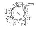
- the apparatus illustrated in Figure 1 comprises as liquid applicator means one or more nozzles which dispense the liquid developer in a ditribution pattern corresponding to a lower resolution version of the electrostatic image to be developed.
- the dispensing of liquid by said nozzles is controlled by sequential electrical signals that are modulated in strength in dependence on digitized information representing elementary picture parts (pixels) of the lower resolution pattern.
- element 1 represent a conductive drum rotationally driven by its shaft 2.
- a photoconductive coating 3 e.g. made of vapour-deposited photoconductive selenium or selenium alloy, is present.
- the photoconductive layer 3 is overall charged electrostatically with the direct current corona unit 4.
- the photoconductive layer 3 is scanning-wise exposed by means of an array 5 of LED elements of which the light-output is controlled by digital signals fed to the array by input line 6 which is connected to the signal output of a character generator (not shown in the drawing).
- the photoconductive layer 3 in moving past the LED array 5 is irradiated by tiny light spots corresponding with the light-emissions from the individually modulated LED elements in the array 5.
- the layer 3 is in that way discharged pattern-wise at a resolution of 16 lines per mm.
- the ink-jet operates according to a known principle involving piezo-electric deformation of individual ink-jet channels arranged in a row a described e.g. in "Druck Print” 1 (1981), p. 24.
- the piezo-electric crystals are activated by electronic signals stemming from the character generator but in such a way that the liquid developer is dispensed in a distribution pattern corresponding to a coarser version of the electrostatic image formed on layer 3 by the scanning-wise exposure.
- the coarser distribution pattern can e.g. be one resulting from the integration of four neighbouring digitized pixel values, and the deposition of overlapping drops, so that the resolution of the distribution pattern is four times lower than of the said electrostatic image.
- a light source 9 that overall illuminates the photoconductive layer 3 to a level sufficient to remove residual charge in the background area to prevent toner deposition thereon in the following air-jet cleaning.
- Surplus liquid and toner particles not held electrostatically by the photoconductive layer 3 are removed with an air-jet by blowing pressurized air in the intake 10 of the venturi shaped passage 11 towards the outlet 12.
- the outlet 12 is connected to a vacuum pump. Upstream of the pump a filter withholds toner particles and a vapour trap, e.g. activated carbon, captures vaporized carrier liquid.
- a vapour trap e.g. activated carbon
- the toner particle image left on photoconductive layer 3 is transferred under the influence of electrostatic charges of opposite polarity generated by transfer corona 13 to a receiving paper sheet 14.
- Individual paper sheets 14 are supplied from a sheet dispenser 15 and are conveyed by a series of conveyor rollers 16 towards a pivotable receiving tray 17.
- the photoconductive layer 3 after transfer of the toner image is overall exposed to light source 18 to remove residual charges and is cleaned with web device 19 to remove residual toner.
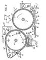
- the apparatus illustrated in Figure 2 comprises a photoconductive carrier drum 20 which is arranged in close proximity to a drum 1 corresponding to drum 1 in Figure 1.
- the drum 20 is rotationally driven by its shaft 21.
- the drum comprises a conductive shell made e.g. from a aluminium, which bears a photoconductive coating 22, e.g. made of vapour-deposited photoconductive selenium or selenium alloy.
- a photoconductive coating 22 e.g. made of vapour-deposited photoconductive selenium or selenium alloy.
- the photoconductive layer 22 is overall charged electrostatically with the direct current corona unit 23.
- the photoconductive layer 22 is line-wise exposed by means of an array 24 of LED elements of which the light-output is controlled by digital signals fed to the array by input line 25 which is connected to the signal output of a character genteator (not shown in the drawing).
- the LED array irradiates the photoconductive layer in a pattern of spots of larger diameter than the spots irradiated on photodonductive layer 3, by the LED array 5.
- the electrostatic charge pattern thus formed on drum 20 corresponds with the electrostatic image formed on drum 1 but is of lower resolution.
- electrophoretic developer liquid 27 is flowed through a passage 28 defined by a developing electrode 29 and the photoconductive layer 22 and developer is image-wise attracted to the drum to develop the electrostatic charge pattern thereon.
- the developing device is provided with a liquid recycling pump 36.
- a conductive bar 30 that is connected to a direct current voltage source 31 and thereby induces through the conductive material of the drum and the photoconductive layer 22 a charge at least partially neutralizing the electrostatic charges by which the toner particles are attracted to the drum 20.
- the charges forming the electrostatic image on photoconductive layer 3 provide the necessary electrical field strength to cause the toner partices to transfer, i.e. jump across the gap between the photoconductive layer 22 and the photoconductive layer 3 and to develop the said electrostatic image.
- the width of the gap is not very critical and may be in the range of 10 to 50 um yielding a sharp development.
- the peripheral speed of the drums 1 and 20 is the same but their motions at the location of the development zone i.e. at the toner transfer gap, are in opposite directions.
- the photoconductive layer 22 after said transfer of toner particles is cleaned with web 32 of cleaning device 33 to remove residual toner developer.
- Residual charge on photoconductive layer 22 is removed by overall illumination with exposure source 34 and treatment with the ionizing flux of the alternating current corona 35.
- the apparatus illustrated in Figure 3 is similar to that shown in Figure 2 except that a dielectric belt 42 carries the initially formed pattern of liquid developer to the development zone.
- the dielectric belt 42 is supported by a conductive drum 40 and a pulley 43.
- the drum is driven anti-clockwise by its shaft 41.
- the drum 1 can e.g. be made of a aluminium.
- the dielectric belt 42 can e.g. be formed by polyethylene-coated paper.
- the belt 42 is pattern-wise charged with a cathode ray tube 44 having one or more rows of closely spaced fine wires 45 embedded in the face of the tube as described in the book "Electrophotgraphy" by R.M. Schaffert, second revised edition, The Focal Press, London and New York, (1975), pp. 205-206.
- the belt 42 is sandwiched between the face of the tube 44 and a grounded electrode 46.
- the charge pattern thus formed on the belt corresponds with the electrostatic image formed on the surface of photoconductive layer 3 (which is the image to be developed) but is of a lower resolution.
- the preliminary development by the developing device 26, the transfer of liquid developer to the drum 1, and the operations of the cleaning web 32 and the corona 35 take place in the same way as in the apparatus according to Figure 2.
- the peripheral speed of the drums 1 and 40 is the same but their motions at the location of the tone transfer gap are in the opposite directions.
- a dielectric web supplied from a spool can be used instead of an endless dielectric belt. In that case cleaning operations can be omitted because in each copying cycle a fresh frame of the web can be used.
- an ink-jet dispenser can be used for dispensing liquid developer in the required relatively low resolution image pattern onto a dielectric member to form thereon the liquid developer pattern and this pattern can be progressively brought to the development zone for developing the higher resolution electrostatic image on the recording surface.
- the ink-jet device of the embodiment illustrated in Figure 1 can be used to form a coarse liquid developer pattern on a dielectric carrier roller and the toner particles of that pattern can be transferred onto the electrostatic image of higher image resolution formed on the photconductive drum 1 in that figure.
- This latter procedure has the advantage in comparison with tray development that a fresh portion of liquid developer is made available for the development in each copying cycle. So there is no need for toner replenishment. Changes in developer properties due to accumulation of dissolved charge controlling ions, as takes place in tray development, do not take place.
- the liquid developer is supplied pattern-wise and does not wet the whole surface of the carrier roller, less carrier liquid has to be removed in the fixing step. Consequently there is less environmental pollution and a hydrocarbon carrier liquid for the toner particles can be used with practically no risk of fire.
- the photoconductive layer and its conductive support may form a fixed part of a rotating drum or may be constructed by sheet material which is removably attached to a drum.
- the photoconductive member can be in the form of a belt, e.g. an endless belt, that can be replaced.
Landscapes
- Physics & Mathematics (AREA)
- General Physics & Mathematics (AREA)
- Wet Developing In Electrophotography (AREA)
Claims (15)
Priority Applications (4)
| Application Number | Priority Date | Filing Date | Title |
|---|---|---|---|
| EP86200841A EP0246362B1 (de) | 1986-05-15 | 1986-05-15 | Verfahren und Gerät zur Entwicklung eines elektrostatischen Ladungsbildes |
| DE8686200841T DE3676693D1 (de) | 1986-05-15 | 1986-05-15 | Verfahren und geraet zur entwicklung eines elektrostatischen ladungsbildes. |
| US07/044,418 US4770967A (en) | 1986-05-15 | 1987-04-30 | Method and apparatus for the development of an electrostatic charge image |
| JP62116684A JPS62278583A (ja) | 1986-05-15 | 1987-05-13 | 静電荷像の現像方法および装置 |
Applications Claiming Priority (1)
| Application Number | Priority Date | Filing Date | Title |
|---|---|---|---|
| EP86200841A EP0246362B1 (de) | 1986-05-15 | 1986-05-15 | Verfahren und Gerät zur Entwicklung eines elektrostatischen Ladungsbildes |
Publications (2)
| Publication Number | Publication Date |
|---|---|
| EP0246362A1 EP0246362A1 (de) | 1987-11-25 |
| EP0246362B1 true EP0246362B1 (de) | 1990-12-27 |
Family
ID=8195738
Family Applications (1)
| Application Number | Title | Priority Date | Filing Date |
|---|---|---|---|
| EP86200841A Expired EP0246362B1 (de) | 1986-05-15 | 1986-05-15 | Verfahren und Gerät zur Entwicklung eines elektrostatischen Ladungsbildes |
Country Status (4)
| Country | Link |
|---|---|
| US (1) | US4770967A (de) |
| EP (1) | EP0246362B1 (de) |
| JP (1) | JPS62278583A (de) |
| DE (1) | DE3676693D1 (de) |
Families Citing this family (4)
| Publication number | Priority date | Publication date | Assignee | Title |
|---|---|---|---|---|
| US5378574A (en) * | 1988-08-17 | 1995-01-03 | Xerox Corporation | Inks and liquid developers containing colored silica particles |
| US4918487A (en) * | 1989-01-23 | 1990-04-17 | Coulter Systems Corporation | Toner applicator for electrophotographic microimagery |
| US5121131A (en) * | 1989-10-30 | 1992-06-09 | Drexler Technology Corporation | Instant high contrast imaging system |
| DE19634088C2 (de) * | 1996-08-23 | 2002-02-14 | Roland Man Druckmasch | Vorrichtung zum bilddifferenzierten Einfärben eines latenten elektrostatischen Bildes |
Family Cites Families (8)
| Publication number | Priority date | Publication date | Assignee | Title |
|---|---|---|---|---|
| US3052213A (en) * | 1958-12-17 | 1962-09-04 | Ibm | Electrostatic printer apparatus for printing with liquid ink |
| US3216844A (en) * | 1962-03-02 | 1965-11-09 | Xerox Corp | Method of developing electrostatic image with photoconductive donor member |
| US3512965A (en) * | 1963-07-12 | 1970-05-19 | Australia Res Lab | Electroprinting method |
| US3656173A (en) * | 1969-08-08 | 1972-04-11 | Olivetti & Co Spa | Liquid development of electrostatic images |
| US4058637A (en) * | 1971-02-18 | 1977-11-15 | Research And Development Laboratories Of Ohno Co., Ltd. | Electrostatic developing method |
| US3888666A (en) * | 1971-12-22 | 1975-06-10 | Rank Xerox Ltd | Reversal developing method using photoconductive developing electrode |
| US4268597A (en) * | 1976-04-13 | 1981-05-19 | Philip A. Hunt Chemical Corp. | Method, apparatus and compositions for liquid development of electrostatic images |
| JPS5484738A (en) * | 1977-12-19 | 1979-07-05 | Ricoh Co Ltd | Developing device for variable magnification copier |
-
1986
- 1986-05-15 DE DE8686200841T patent/DE3676693D1/de not_active Expired - Fee Related
- 1986-05-15 EP EP86200841A patent/EP0246362B1/de not_active Expired
-
1987
- 1987-04-30 US US07/044,418 patent/US4770967A/en not_active Expired - Fee Related
- 1987-05-13 JP JP62116684A patent/JPS62278583A/ja active Pending
Also Published As
| Publication number | Publication date |
|---|---|
| DE3676693D1 (de) | 1991-02-07 |
| JPS62278583A (ja) | 1987-12-03 |
| US4770967A (en) | 1988-09-13 |
| EP0246362A1 (de) | 1987-11-25 |
Similar Documents
| Publication | Publication Date | Title |
|---|---|---|
| US4769676A (en) | Image forming apparatus including means for removing residual toner | |
| EP0010375B1 (de) | Elektrostatographisches Gerät | |
| EP0096978B1 (de) | Gerät zur elektrographischen Bilderzeugung | |
| US3645614A (en) | Aperture-controlled electrostatic printing system employing ion projection | |
| US4833503A (en) | Electronic color printing system with sonic toner release development | |
| US5826147A (en) | Electrostatic latent image development | |
| EP0240888B1 (de) | Elektrophotographisches Farbverfahren und Gerät | |
| JPH11295981A (ja) | 低付着性トナ―を搬送するためのイオン充電式現像システム | |
| JP2645078B2 (ja) | 液体像転写装置 | |
| JPH03200271A (ja) | 現像装置 | |
| JPH0652451B2 (ja) | 液体現像装置 | |
| EP0532306B1 (de) | System zum Entfernen von Agglomeraten von einem, auf einem Photorezeptor entwickelten, Bildes | |
| EP0246362B1 (de) | Verfahren und Gerät zur Entwicklung eines elektrostatischen Ladungsbildes | |
| GB2036605A (en) | Developing latent electrostatic images | |
| US5084718A (en) | Wet recording apparatus and wet recording method | |
| JPH08234614A (ja) | ストリークの除去工程を備えたカラー透明体定着装置および構造 | |
| CA1327834C (en) | Laser addressed ionography | |
| CA1223297A (en) | Xerographic apparatus and process with backside photoconductor imaging | |
| US5826149A (en) | Developing device employing a liquid developer and picture forming device having such developing device | |
| JPS6064364A (ja) | 画像形成方法および装置 | |
| US4144061A (en) | Transfer development using a fluid spaced donor member | |
| US6102523A (en) | Printer for large format printing using a direct electrostatic printing (DEP) engine | |
| US5420672A (en) | Concept for prevention of scavengeless nip wire contamination with toner | |
| US5077172A (en) | Carrier web transfer device and method for electrophotographic printing press | |
| JPS6118972A (ja) | 光導電性トナ−を用いる記録方法 |
Legal Events
| Date | Code | Title | Description |
|---|---|---|---|
| PUAI | Public reference made under article 153(3) epc to a published international application that has entered the european phase |
Free format text: ORIGINAL CODE: 0009012 |
|
| AK | Designated contracting states |
Kind code of ref document: A1 Designated state(s): AT BE CH DE FR GB IT LI LU NL SE |
|
| RBV | Designated contracting states (corrected) |
Designated state(s): BE DE FR GB |
|
| 17P | Request for examination filed |
Effective date: 19880413 |
|
| 17Q | First examination report despatched |
Effective date: 19900405 |
|
| GRAA | (expected) grant |
Free format text: ORIGINAL CODE: 0009210 |
|
| AK | Designated contracting states |
Kind code of ref document: B1 Designated state(s): BE DE FR GB |
|
| REF | Corresponds to: |
Ref document number: 3676693 Country of ref document: DE Date of ref document: 19910207 |
|
| ET | Fr: translation filed | ||
| PGFP | Annual fee paid to national office [announced via postgrant information from national office to epo] |
Ref country code: FR Payment date: 19910423 Year of fee payment: 6 |
|
| PGFP | Annual fee paid to national office [announced via postgrant information from national office to epo] |
Ref country code: BE Payment date: 19910425 Year of fee payment: 6 |
|
| PGFP | Annual fee paid to national office [announced via postgrant information from national office to epo] |
Ref country code: GB Payment date: 19910430 Year of fee payment: 6 |
|
| PGFP | Annual fee paid to national office [announced via postgrant information from national office to epo] |
Ref country code: DE Payment date: 19910502 Year of fee payment: 6 |
|
| PLBE | No opposition filed within time limit |
Free format text: ORIGINAL CODE: 0009261 |
|
| STAA | Information on the status of an ep patent application or granted ep patent |
Free format text: STATUS: NO OPPOSITION FILED WITHIN TIME LIMIT |
|
| 26N | No opposition filed | ||
| PG25 | Lapsed in a contracting state [announced via postgrant information from national office to epo] |
Ref country code: GB Effective date: 19920515 |
|
| PG25 | Lapsed in a contracting state [announced via postgrant information from national office to epo] |
Ref country code: BE Effective date: 19920531 |
|
| BERE | Be: lapsed |
Owner name: AGFA-GEVAERT N.V. Effective date: 19920531 |
|
| GBPC | Gb: european patent ceased through non-payment of renewal fee |
Effective date: 19920515 |
|
| PG25 | Lapsed in a contracting state [announced via postgrant information from national office to epo] |
Ref country code: FR Effective date: 19930129 |
|
| PG25 | Lapsed in a contracting state [announced via postgrant information from national office to epo] |
Ref country code: DE Effective date: 19930202 |
|
| REG | Reference to a national code |
Ref country code: FR Ref legal event code: ST |