EP0247871A2 - Variable Phasenverschiebungsschaltung - Google Patents
Variable Phasenverschiebungsschaltung Download PDFInfo
- Publication number
- EP0247871A2 EP0247871A2 EP87304725A EP87304725A EP0247871A2 EP 0247871 A2 EP0247871 A2 EP 0247871A2 EP 87304725 A EP87304725 A EP 87304725A EP 87304725 A EP87304725 A EP 87304725A EP 0247871 A2 EP0247871 A2 EP 0247871A2
- Authority
- EP
- European Patent Office
- Prior art keywords
- current
- voltage
- output
- phase
- conversion means
- Prior art date
- Legal status (The legal status is an assumption and is not a legal conclusion. Google has not performed a legal analysis and makes no representation as to the accuracy of the status listed.)
- Granted
Links
Images


Classifications
-
- G—PHYSICS
- G05—CONTROLLING; REGULATING
- G05F—SYSTEMS FOR REGULATING ELECTRIC OR MAGNETIC VARIABLES
- G05F3/00—Non-retroactive systems for regulating electric variables by using an uncontrolled element, or an uncontrolled combination of elements, such element or such combination having self-regulating properties
- G05F3/02—Regulating voltage or current
-
- H—ELECTRICITY
- H03—ELECTRONIC CIRCUITRY
- H03H—IMPEDANCE NETWORKS, e.g. RESONANT CIRCUITS; RESONATORS
- H03H11/00—Networks using active elements
- H03H11/02—Multiple-port networks
- H03H11/16—Networks for phase shifting
- H03H11/20—Two-port phase shifters providing an adjustable phase shift
Definitions
- the present invention relates to a variable phase shifting circuit which is capable of controlling the phase of an output signal with respect to an input signal suitable for use in electronic equipment by a control voltage (or current).
- phase shift range is limited to 90 degrees from +45 to -45 degrees and the amplitude also varies according as the phase shift angle changes.
- An object of the present invention is to provide a variable phase shifting circuit which is capable of shifting the phase over a range broader than 90 degrees, and which has no possibility that the amplitude changes in dependence upon the phase shift angle.
- the present invention provides a variable phase shifting circuit comprising a phase splitter for distributing an input signal into first and second signals which are 90 degrees out of phase to output them, a first double balanced differential amplifier to which a first output signal from the phase splitter is delivered as an input signal, a second double balanced differential amplifier to which a second output signal from the phase splitter is delivered as an input signal, a summer for summing respective output signals from the first and second double balanced differential amplifiers to output the summed result, a converter for converting a control input to differential currents, first logarithmic conversion means for converting an output current of the converter to a logarithmic voltage, circular function conversion means for converting the output current of the converter to circular function, and second logarithmic conversion means for converting an output current of circular function conversion means to a logarithmic voltage, thus to control the gain of the first double balanced differential amplifier using an output from the first logarithmic conversion means and to control the gain of the second double balanced differential amplifier using an output from the second logarithmic
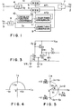
- Fig. 7 is a circuit diagram of an example of a voltage controlled phase shifting circuit illustrated as an example of the background art variable phase shifting circuit.
- the voltage controlled phase shifting circuit of the background art configuration shown in Fig. 7 includes a signal input terminal I, a signal output terminal 2, an input terminal 3 for a control voltage, a phase shifter of +45 degrees designated at 12, and a phase shifter of -45 degrees designated at 13 wherein an input signal Vi is delivered to the two phase shifters of 45 degrees through the input terminal I.
- the phase shifter 12 delivers an output signal V a obtained by shifting the phase of a signal input thereto by an angle an of +45 degrees to the base of a transistor Q a .
- the phase shifter 13 delivers an output signal V b obtained by shifting the phase of the signal input thereto by an angle of -45 degrees to the base of a transistor Q b .
- the transistors Q a and Q b of which emitters are grounded through individual emitter resistors R a output currents i a and i b in correspondence with the signals V a and Vb delivered to their bases, respectively.
- indication of the base bias voltages for the transistors Q a and Q b is omitted for the brevity of the explanation.
- the above-mentioned current i a flowing in the transistor Q a branches at control transistors Q c and Q d .
- the above-mentioned current i b flowing in the transistor Q b branches at control transistors Qe and Q f .
- a control voltage V x delivered to the input terminal 3 for the control voltage is applied to the bases of the above-mentioned transistors Q d and Q e .
- a reference voltage V R is applied from a reference power source VR to the bases of the above-mentioned transistors Qc and Q f .
- the currents separately flowing in the respective transistors Q c to Q f vary in accordance with the control voltage V x .
- the branch ratio in respect of the transistor Q d in the control transistors Q c and Q d at which the current i a of the transistor Q a branches is represented by a p (O ⁇ p ⁇ I) and the branch ratio in respect of the transistor Q f in the control transistors Q e and Q f at which the current i b of the transistor Q b branches is respresented by q (0 ⁇ q ⁇ I).
- the output current of the transistor Q d is expressed as p i a
- the output current of the transistor Q f is expressed as q i b .
- a current flowing through the load resistor R b is expressed as p i a + q i b .
- the output current ia of the transistor Q d has a phase angle of +45 degrees with respect to the input voltage Vi and the output current i b of the transistor Q f has a phase angle of -45 degrees with respect to the input voltage Vi.
- the center phase of the output voltage V o varies, as shown in Fig. 8, within a range of ⁇ 45 degrees with respect to the input voltage V i in accordance with the above-mentioned branch ratios p and q.
- the output voltage V o output from the voltage controlled phase shifting circuit of the background art has a characteristic such that its phase varies according as the control voltage changes and its amplitude also varies at the same time.
- the amplitude at the both ends of the phase control range is increased to a value obtained by multiplying the amplitude at the central position of the phase control range by V2, and the phase control range is limited to substantially ⁇ 45 degrees.
- the voltage controlled phase shifting circuit exhibiting such a phase control characteristic is applicable to a voltage controlled oscillator etc., this circuit cannot be used as a phase shifting circuit in the application field in which it is required that the signal phase can be arbitrarily controlled and the amplitude of the output voltage does not change still at the time when the signal is subjected to phase control.
- Fig. I is a block diagram illustrating an example of the configuration of a variable phase shifting circuit according to the present invention implemented as a voltage controlled phase shifting circuit.
- This phase shifting circuit includes a signal input terminal I, a signal output terminal 2, an input terminal 3 for the control voltage, a phase splitter 4, double balanced differential amplifiers 5 and 6, a summer 7, a voltage-to-current converter 8, logarithmic conversion means 9 and II, and circular function conversion means 10.
- the phase splitter 4 responds to the input signal Videlivered through the input terminal I to generate two signals V i and V 2 which are 90 degrees out of phase to output them.
- One signal Vi of the two signals V 1 and V 2 output from the phase splitter 4 is delivered to the first double balanced differential amplifier 5 as an input signal.
- the other signal V 2 thereof is delivered to the second double balanced differential amplifier 6.
- the double balanced differential amplifier 5 is subjected to gain control by a control voltage AV 1 delivered thereto.
- the double balanced differential amplifier 6 is subjected to gain control by a control voltage ⁇ V2 delivered thereto.
- Output signals from the first and second double balanced differential amplifiers 5 and 6 are subjected to vector summation at a summer 7.-The summed value is output to the output terminal 2 as an output signal Vo.
- the control voltage Vx delivered to a voltage-to-current converter 8 through the input terminal 3 is converted to a current l x at the voltage-to-current converter 8.
- the current l x thus obtained is output to the logarithmic conversion means 9 and to the circular function conversion means 10.
- the current I x output from the voltage-to-current converter 8 is changed to a control voltage ⁇ V 1 by the logarithmic conversion means 9.
- This control voltage ⁇ V 1 is used for the gain control of the first double balanced differential amplifier 5.
- the first and second double balanced differential amplifiers 5 and 6 are subjected to the gain control by the control voltage ⁇ V 1 and AV 2 , respectivley.
- an output signal V o having a fixed amplitude is output within the range of a phase angle of ⁇ 90 degrees.
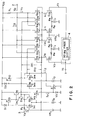
- Fig. 2 is a circuit diagram illustrating an actual circuit arrangement of a variable phase shifting circuit according to the present invention implemented as a voltage controlled phase shifting circuit.
- a phase shifter of 90 degrees is used as the phase splitter 4.
- the first and second output signals V i and V 2 are output from the phase splitter 4.
- the first output signal V i has a phase difference of 90 degrees with respect to an input signal V i and the second output signal V 2 is in phase with the input signal Vi.
- the circuit configuration including transistors Q 17 to Q 22 , two resistors R e and a current source II constitutes a well known double balanced differential amplifier.
- This double balanced differential amplifier corresponds to the first double balanced differential amplifier 5 in the voltage controlled phase shifting circuit shown in Fig. I.
- the well known double balanced operational amplifier including transistors Q 11 to Q 16 , two resistors R e and a current source II corresponds to the second balanced differential amplifier in the voltage controlled phase shifting circuit shown in Fig. I.
- the first output signal V i of the two output signals output from the above-mentioned phase splitter 4 is delivered to the base of the transistor Q 22 .
- the second output signal V 2 thereof is delivered to the base of the transistor Q 11 .
- a reference bias voltage V R2 from a reference bias power source VR2 is delivered. While the above-mentioned two signals V i and V 2 include the reference bias voltage VR 2 as a matter of cource, the indication of the circuit configuration therefor is omitted for the brevity of illustration.
- the outputs of the first and second double balanced differential amplifiers 5 and 6 are output from the commonly connected collectors of the transistors Q 18 and Q 2 o and the commonly connected collectors of the transistors Qi4 and Q 16 as output currents i c1 and ic2, respectively.
- the both output currents are summed at the commonly connected load resistor R L .
- an output voltage V o is output to the output terminal 2.
- the gain of the first double balanced differential amplifier 5 is controlled by the control voltage ⁇ V 1 applied across the bases of the paired transistors Qi and Q 18 and across those of the paired transistors Qi and 0 20 .
- the gain of the second double balanced differential amplifier 6 is controlled by the control voltage AV 2 applied across the bases of the paired transistors Q 13 and Qi 4 and across those of the paired transistors Qis and Q 16 .
- the circuit configuration including a resistor R 1 , transistors Qi to Q 4 , a diode Di, a current source l o , and a reference voltage source VRI corresponds to the voltage-to-current converter 8 and the logarithmic conversion means 9 in the voltage controlled phase shifting circuit shown in Fig. I.
- the control voltage AV 1 determined with the reference voltage VRI set at the reference voltage source VRI being as reference is delivered from the collector of the transistor Q 2 to the control terminal of the first double balanced differential amplifier 5.
- the circuit configuration including transistors Q 2 and Q 4 to Q 7 , and a diode D 2 constitutes the circular function conversion means 10 in the voltage controlled phase shifting circuit shown in Fig. I.
- the circuit configuration including transistors Q 8 to Q 10 , a diode D 3 and a current source I o constitutes the logarithmic conversion means II in the voltage controlled phase shifting circuit shown in Fig. I.
- the control voltage ⁇ V 2 determined with the reference voltage V R1 set at the reference voltage source VRI being as reference is delivered from the collector of the transistor Q 9 to the control terminal of the second double balanced differential amplifier 6.
- control voltage V x applied to the input terminal 3 for the control voltage is determined with the reference voltage V R1 set at the reference voltage source VRI as reference.
- this control voltage V x is converted to a control current I x flowing into the collector of the transistor Q 2 (or flowing out from the collector of the transistor Q 2 ) through the resistor Rl.
- the circuit comprising the transistors Qi and Q 2 paired for constituting the differential amplifier and the current source l o and a current mirror circuit comprising the diode D 1 and the transistor Q 3 constitutes a well known differential amplifier operative with the current mirror circuit being as the load.
- the output of the differential amplifier obtained at the collector of the transistor Q 2 is fed back to the base of the transistor Q 2 , which serves as the inverting input terminal of the differential amplifier.
- the reference voltage source VRI is connected to the base of the transistor Qi, which serves as the non-inverting input terminal of the differential amplifier.
- the output ⁇ V 1 corresponding to the output of the logarithmic conversion means 9 in the voltage controlled phase shifting circuit shown in Fig. I, i.e., the control voltage ⁇ V 1 is obtained from the collector (base) of one transistor Q 2 of the transistor pair for constituting the differential amplifier with the reference voltage VR of the reference voltage source VRI being as reference.
- control voltage ⁇ V 1 is regarded as a voltage obtained by applying logarithmic conversion to the control current I x .
- the circuit configuration including the transistors Q 2 , Q 4 to Q 7 , and the diode D 2 constitutes the circular function conversion means 10 in the voltage controlled phase shifting circuit shown in Fig. I.
- the base of the NPN transistor Qs is connected to the emitter of the transistor Q 4 .
- the base of the PNP transistor Q 6 is connected to the emitters of the differential Q 1 and Q 2 paired for constituting the differential amplifier.
- emitters of the transistors Q 5 and Q 6 are connected to each other.
- the base-emitter voltages of the transistors Q 4 , Qs and Q 6 are designated by V BE4 , V BE5 and V BES , respectively
- the following equation (3) holds in connection with the base-emitter voltages of the transistors Qs and Q 6 :
- the base-emitter voltages V BE of the respective transistors are expressed by the following equation (4): where I s1 and I s2 denote saturation currents of the NPN transistor Q 5 and the PNP transistor Q 6 , respectively.
- the currents I e1 and le 2 flow in the transistors Q 4 and Q 2 , respectively.
- the current ly is amplified by the current mirror circuit comprising the diode D 2 and the transistor Q 7 and is then output as a current I z .
- the relationship between the currents I z and ly 21y. Accordingly, from the aquation (5), the current I z is expressed as follows: Namely, Iz is the circular function of I x .
- the current I z which has undergone the circular function conversion is converted, at the logarithmic conversion means II, to the differential currents l e8 and l e9 as explained with reference to the circuit shown in Fig. 3 and is then subjected to logarithmic conversion.
- a control voltage AV 2 determined with the reference voltage V R1 of the reference voltage source VRI being as reference is output from the logarithmic conversion means II as indicated by the following equation (7):
- an input signal V 2 is subjected to current conversion at the second double balanced differential amplifier 6.
- signal currents i 2 and i 2 flow in the transistors Q 11 and Q 12 , respectively.
- These signal currents i 2 and -i 2 flow in the load resistor R L as a current i c2 on the basis of the operation of the circuit comprising transistors Q 13 to Q 16 of which branch ratio n is controlled by the control voltage ⁇ V 2 .
- a summed current of the currents i c1 and i c2 flows in the load resistor R L .
- an output signal V o is output.
- the following equations hold in connection with these signal currents and the output voltage: and
- FIG. 6 shows another embodiment of the circuit configuration of the voltage-to-current converter 8, the logarithmic conversion means 9 and the circular function conversion means 10 in the voltage controlled phase shifting circuit of the first embodiment shown in Fig. I.
- the circuit configuration including transistors Q 23 and Q 24 paired for constituting the differential amplifier, two current sources 1 0 , and a resistor R 2 is a well known differential amplifier. This portion constitutes the voltage-to-currerit converter 8.
- a control voltage Vx is input to the base of the transistor Q 23 through the input terminal 3, and the reference voltage V R3 set at the reference voltage source VR3 is applied to the base of the transistor Q 24 .
- a reference voltage source VR4 is commonly connected to the bases of transistors Q 25 and Q 26 which constitute the logarithmic conversion means, and a control voltage AV 1 appears across the emitters of the transistors Q 25 and 0 26 .
- a current mirror circuit composed of a diode D 4 and a transistor Q 27 and a circuit composed of transistors 0 26 and Q 28 to 0 31 , and a diode Ds constitute the circular function conversion means 10, thus to output from the transistor 3I a current I z which has been converted to the circular function.
- the operation of the circuit shown in Fig. 6 is as follows.
- the base-emitter voltages VB E of the transistors Q 25 and Q 26 vary, and the control voltage ⁇ V 1 expressed as the equation (2) as its difference voltage is obtained across the both emitters.
- a current equal to the current l e25 flowing in the transistor Q 25 is output from the transistor Q 27 .
- the current thus output flows in the transistor Q 28 .
- the bases and the collectors of the transistors Q 28 and Q 26 are commonly connected to the reference voltage source VR4, the sum of the base-emitter voltages V BE28 and V BE26 of the transistors Q 28 and Q 26 is applied across the bases of the transistors Q 29 and 0 30 .
- variable phase shifting circuit is configured as the voltage controlled phase shifting circuit.
- the variable phase shifting circuit when there is employed an arrangement such that the phase control is effected using a control input current instead of the voltage-to-current converter, the variable phase shifting circuit may be implemented as the current controlled phase shifter.
- a phase splitter to output two signals which are phase-shifted, for example, by ⁇ 45 degrees. In such a case, while the central value of the phase of the output signal is shifted by a suitable value with respect to the input, it is needless to say that the manner of the phase control is the same as in the above-mentioned embodiments.
- variable phase shifting circuit comprises a phase splitter for distributing an input signal into first and second signals which are 90 degrees out of phase to output them, a first double balanced differential amplifier to which a first output signal from the phase splitter is delivered as an input signal, a second double balanced differential amplifier to which a second output signal from the phase splitter is delivered as an input signal, a summer for summing respective output signals from the first and second double balanced differential amplifier to output the summed result, a converter for converting a control input to differential currents, first logarithmic conversion means for converting an output current of the converter to a logarithmic voltage, circular function conversion means for converting the output current of the converter to a circular function, and second logarithmic conversion means for converting an output current of the circular function conversion means to a logarithmic voltage, thus to control the gain of the first double balanced differential amplifier using an output from the first logarithmic conversion means, and to control the gain of the second double balanced differential amplifier using an output
- the present invention by changing the control input in directions of positive and negative going swings with respect to the reference voltage, under condition where the amplitude of the output signal remains fixed, it is possible to easily realize a variable phase shifting circuit capable of changing the phase within a range of ⁇ 90 degrees.
- the present invention can advantageously solve problems with the above-described variable phase shifting circuit of the background art.
Landscapes
- Engineering & Computer Science (AREA)
- Physics & Mathematics (AREA)
- Electromagnetism (AREA)
- General Physics & Mathematics (AREA)
- Radar, Positioning & Navigation (AREA)
- Automation & Control Theory (AREA)
- Networks Using Active Elements (AREA)
- Amplifiers (AREA)
- Tone Control, Compression And Expansion, Limiting Amplitude (AREA)
Applications Claiming Priority (2)
| Application Number | Priority Date | Filing Date | Title |
|---|---|---|---|
| JP61124179A JPS62281506A (ja) | 1986-05-29 | 1986-05-29 | 可変移相回路 |
| JP124179/86 | 1986-05-29 |
Publications (3)
| Publication Number | Publication Date |
|---|---|
| EP0247871A2 true EP0247871A2 (de) | 1987-12-02 |
| EP0247871A3 EP0247871A3 (en) | 1989-08-16 |
| EP0247871B1 EP0247871B1 (de) | 1993-03-31 |
Family
ID=14878929
Family Applications (1)
| Application Number | Title | Priority Date | Filing Date |
|---|---|---|---|
| EP87304725A Expired - Lifetime EP0247871B1 (de) | 1986-05-29 | 1987-05-28 | Variable Phasenverschiebungsschaltung |
Country Status (5)
| Country | Link |
|---|---|
| US (1) | US4737703A (de) |
| EP (1) | EP0247871B1 (de) |
| JP (1) | JPS62281506A (de) |
| KR (1) | KR900004765B1 (de) |
| DE (1) | DE3785082T2 (de) |
Cited By (4)
| Publication number | Priority date | Publication date | Assignee | Title |
|---|---|---|---|---|
| EP0355329A3 (en) * | 1988-08-25 | 1990-08-22 | Ant Nachrichtentechnik Gmbh | Method and circuit for phase shifting |
| EP0334493A3 (de) * | 1988-03-25 | 1990-09-19 | Tektronix Inc. | Verzögerungsschaltung für eine Uhr mit kontinuierlicher Regelung |
| GB2283872A (en) * | 1993-11-12 | 1995-05-17 | Northern Telecom Ltd | Frequency multipliers |
| RU2273950C2 (ru) * | 2003-11-19 | 2006-04-10 | Новочеркасский военный институт связи | Устройство управления фазой колебаний |
Families Citing this family (8)
| Publication number | Priority date | Publication date | Assignee | Title |
|---|---|---|---|---|
| JPH07114382B2 (ja) * | 1986-11-18 | 1995-12-06 | 日本電気株式会社 | 携帯無線機用車載アダプタ− |
| US5317200A (en) * | 1991-09-30 | 1994-05-31 | Sony Corporation | Phase shift circuit apparatus |
| US5736840A (en) * | 1993-09-09 | 1998-04-07 | Kabushiki Kaisha Toshiba | Phase shifter and communication system using the phase shifter |
| JP3410776B2 (ja) * | 1993-09-09 | 2003-05-26 | 株式会社東芝 | 直交信号発生回路 |
| US5705922A (en) * | 1995-03-30 | 1998-01-06 | The Whitaker Corporation | Terminator with voltage regulator |
| AT405584B (de) * | 1995-06-16 | 1999-09-27 | Johann W Kolar | Synchronisation der schaltzustandsänderungen parallelgeschalteter zweipunkt-stromgeregelter leistungselektronischer systeme bei definierter phasenversetzung |
| US5924890A (en) * | 1996-08-30 | 1999-07-20 | The Whitaker Corporation | Electrical connector having a virtual indicator |
| US7728576B1 (en) | 2004-01-07 | 2010-06-01 | The United States Of America As Represented By The Secretary Of The Air Force | Programmable multi-channel amplitude and phase shifting circuit |
Family Cites Families (6)
| Publication number | Priority date | Publication date | Assignee | Title |
|---|---|---|---|---|
| US3056921A (en) * | 1959-02-17 | 1962-10-02 | Ryan Aeronautical Co | Variable frequency passive phase shifter |
| US3436647A (en) * | 1966-05-25 | 1969-04-01 | Honeywell Inc | Phase shifting control by phase comparison of signals |
| US3530365A (en) * | 1967-09-27 | 1970-09-22 | James A Peugh | Phase shifting network for producing a phase of any value from 0 to 360 |
| JPS5341025B2 (de) * | 1972-09-22 | 1978-10-31 | ||
| JPS5533747Y2 (de) * | 1975-04-14 | 1980-08-11 | ||
| US4039930A (en) * | 1976-08-12 | 1977-08-02 | General Electric Company | Remotely controlled phase shifting circuit |
-
1986
- 1986-05-29 JP JP61124179A patent/JPS62281506A/ja active Granted
-
1987
- 1987-05-25 KR KR1019870005152A patent/KR900004765B1/ko not_active Expired
- 1987-05-27 US US07/054,939 patent/US4737703A/en not_active Expired - Lifetime
- 1987-05-28 EP EP87304725A patent/EP0247871B1/de not_active Expired - Lifetime
- 1987-05-28 DE DE87304725T patent/DE3785082T2/de not_active Expired - Lifetime
Cited By (5)
| Publication number | Priority date | Publication date | Assignee | Title |
|---|---|---|---|---|
| EP0334493A3 (de) * | 1988-03-25 | 1990-09-19 | Tektronix Inc. | Verzögerungsschaltung für eine Uhr mit kontinuierlicher Regelung |
| EP0355329A3 (en) * | 1988-08-25 | 1990-08-22 | Ant Nachrichtentechnik Gmbh | Method and circuit for phase shifting |
| GB2283872A (en) * | 1993-11-12 | 1995-05-17 | Northern Telecom Ltd | Frequency multipliers |
| GB2283872B (en) * | 1993-11-12 | 1997-11-12 | Northern Telecom Ltd | A quadrature signal processing circuit and method therefor |
| RU2273950C2 (ru) * | 2003-11-19 | 2006-04-10 | Новочеркасский военный институт связи | Устройство управления фазой колебаний |
Also Published As
| Publication number | Publication date |
|---|---|
| JPH0476528B2 (de) | 1992-12-03 |
| DE3785082D1 (de) | 1993-05-06 |
| EP0247871A3 (en) | 1989-08-16 |
| EP0247871B1 (de) | 1993-03-31 |
| KR900004765B1 (ko) | 1990-07-05 |
| JPS62281506A (ja) | 1987-12-07 |
| US4737703A (en) | 1988-04-12 |
| KR870011520A (ko) | 1987-12-24 |
| DE3785082T2 (de) | 1993-09-30 |
Similar Documents
| Publication | Publication Date | Title |
|---|---|---|
| EP0247871A2 (de) | Variable Phasenverschiebungsschaltung | |
| US4663594A (en) | Electronic phase shifter circuit and method | |
| US4168528A (en) | Voltage to current conversion circuit | |
| US4647839A (en) | High precision voltage-to-current converter, particularly for low supply voltages | |
| GB2050740A (en) | Signal-processing transistor circuitry with intrisic temperature insensitiivty | |
| EP0004099A1 (de) | Elektrisch einstellbare Impedanzschaltung | |
| US6201381B1 (en) | Reference voltage generating circuit with controllable linear temperature coefficient | |
| JPH09219630A (ja) | 差動回路 | |
| EP0565299A1 (de) | Aktiver Doppelgegentaktmischer mit von Eintakt in Gegentakt umwandlenden Spannungstromwandlerschaltungen | |
| US4990846A (en) | Temperature compensated voltage reference circuit | |
| US4362956A (en) | Absolute value circuit | |
| NL8300954A (nl) | Electronisch filter, meer in het bijzonder voor verschillende doeleinden. | |
| US4157493A (en) | Delta VBE generator circuit | |
| JPH0351028B2 (de) | ||
| US3448297A (en) | Analog multiplier | |
| JPH07283652A (ja) | 電圧制御キャパシタ | |
| GB2323728A (en) | Bipolar OTA based on hyperbolic function transformation | |
| EP0090329A1 (de) | Amplitudenmodulator | |
| JPH0462608B2 (de) | ||
| JPH0317455Y2 (de) | ||
| Netbut et al. | New simple square rooting circuits based on translinear current conveyors | |
| JPS62110307A (ja) | 可変利得回路 | |
| KR830000469Y1 (ko) | 신호변환 회로 | |
| JPS6223164Y2 (de) | ||
| RU1826118C (ru) | Амплитудный модул тор |
Legal Events
| Date | Code | Title | Description |
|---|---|---|---|
| PUAI | Public reference made under article 153(3) epc to a published international application that has entered the european phase |
Free format text: ORIGINAL CODE: 0009012 |
|
| AK | Designated contracting states |
Kind code of ref document: A2 Designated state(s): DE FR GB |
|
| PUAL | Search report despatched |
Free format text: ORIGINAL CODE: 0009013 |
|
| AK | Designated contracting states |
Kind code of ref document: A3 Designated state(s): DE FR GB |
|
| 17P | Request for examination filed |
Effective date: 19890927 |
|
| 17Q | First examination report despatched |
Effective date: 19910826 |
|
| GRAA | (expected) grant |
Free format text: ORIGINAL CODE: 0009210 |
|
| AK | Designated contracting states |
Kind code of ref document: B1 Designated state(s): DE FR GB |
|
| REF | Corresponds to: |
Ref document number: 3785082 Country of ref document: DE Date of ref document: 19930506 |
|
| ET | Fr: translation filed | ||
| PLBE | No opposition filed within time limit |
Free format text: ORIGINAL CODE: 0009261 |
|
| STAA | Information on the status of an ep patent application or granted ep patent |
Free format text: STATUS: NO OPPOSITION FILED WITHIN TIME LIMIT |
|
| 26N | No opposition filed | ||
| REG | Reference to a national code |
Ref country code: GB Ref legal event code: IF02 |
|
| PGFP | Annual fee paid to national office [announced via postgrant information from national office to epo] |
Ref country code: FR Payment date: 20060515 Year of fee payment: 20 |
|
| PGFP | Annual fee paid to national office [announced via postgrant information from national office to epo] |
Ref country code: GB Payment date: 20060524 Year of fee payment: 20 |
|
| PGFP | Annual fee paid to national office [announced via postgrant information from national office to epo] |
Ref country code: DE Payment date: 20060525 Year of fee payment: 20 |
|
| REG | Reference to a national code |
Ref country code: GB Ref legal event code: PE20 |
|
| PG25 | Lapsed in a contracting state [announced via postgrant information from national office to epo] |
Ref country code: GB Free format text: LAPSE BECAUSE OF EXPIRATION OF PROTECTION Effective date: 20070527 |