EP0247991A1 - Verfahren und Gerät zur mehrkanaligen Messung und digitalen Registrierung von niederfrequenten physiologischen Signalen geringer Amplitude - Google Patents
Verfahren und Gerät zur mehrkanaligen Messung und digitalen Registrierung von niederfrequenten physiologischen Signalen geringer Amplitude Download PDFInfo
- Publication number
- EP0247991A1 EP0247991A1 EP87870074A EP87870074A EP0247991A1 EP 0247991 A1 EP0247991 A1 EP 0247991A1 EP 87870074 A EP87870074 A EP 87870074A EP 87870074 A EP87870074 A EP 87870074A EP 0247991 A1 EP0247991 A1 EP 0247991A1
- Authority
- EP
- European Patent Office
- Prior art keywords
- signal
- channel
- circuit
- sampling
- signals
- Prior art date
- Legal status (The legal status is an assumption and is not a legal conclusion. Google has not performed a legal analysis and makes no representation as to the accuracy of the status listed.)
- Withdrawn
Links
- 238000000034 method Methods 0.000 title claims abstract description 30
- 230000002093 peripheral effect Effects 0.000 claims abstract description 73
- 230000005540 biological transmission Effects 0.000 claims abstract description 52
- 239000003550 marker Substances 0.000 claims abstract description 11
- 238000012937 correction Methods 0.000 claims abstract description 8
- 238000012544 monitoring process Methods 0.000 claims abstract 2
- 238000005070 sampling Methods 0.000 claims description 78
- 238000006243 chemical reaction Methods 0.000 claims description 26
- 238000005259 measurement Methods 0.000 claims description 15
- 230000003750 conditioning effect Effects 0.000 claims description 11
- 230000001143 conditioned effect Effects 0.000 claims description 7
- 239000004020 conductor Substances 0.000 claims description 7
- 230000004913 activation Effects 0.000 claims description 5
- 230000000694 effects Effects 0.000 claims description 3
- 239000012073 inactive phase Substances 0.000 claims description 3
- 239000012071 phase Substances 0.000 claims description 3
- 238000012545 processing Methods 0.000 claims description 2
- 230000006978 adaptation Effects 0.000 claims 1
- 230000003247 decreasing effect Effects 0.000 claims 1
- 230000001667 episodic effect Effects 0.000 claims 1
- 238000001514 detection method Methods 0.000 abstract description 3
- 230000005669 field effect Effects 0.000 description 14
- 238000002955 isolation Methods 0.000 description 10
- 238000010586 diagram Methods 0.000 description 9
- 230000003213 activating effect Effects 0.000 description 6
- 230000004048 modification Effects 0.000 description 5
- 238000012986 modification Methods 0.000 description 5
- 230000003321 amplification Effects 0.000 description 4
- 238000003199 nucleic acid amplification method Methods 0.000 description 4
- 230000010355 oscillation Effects 0.000 description 4
- 239000003990 capacitor Substances 0.000 description 3
- 238000001914 filtration Methods 0.000 description 3
- 230000009466 transformation Effects 0.000 description 3
- 239000008186 active pharmaceutical agent Substances 0.000 description 2
- 230000008901 benefit Effects 0.000 description 2
- 230000000903 blocking effect Effects 0.000 description 2
- 238000004891 communication Methods 0.000 description 2
- 235000021183 entrée Nutrition 0.000 description 2
- 230000006870 function Effects 0.000 description 2
- 230000002401 inhibitory effect Effects 0.000 description 2
- 230000008520 organization Effects 0.000 description 2
- 230000036279 refractory period Effects 0.000 description 2
- 230000000630 rising effect Effects 0.000 description 2
- 230000001360 synchronised effect Effects 0.000 description 2
- 238000012935 Averaging Methods 0.000 description 1
- 238000013459 approach Methods 0.000 description 1
- 230000008859 change Effects 0.000 description 1
- 238000010276 construction Methods 0.000 description 1
- 230000007547 defect Effects 0.000 description 1
- 230000001934 delay Effects 0.000 description 1
- 230000004069 differentiation Effects 0.000 description 1
- 230000009365 direct transmission Effects 0.000 description 1
- 238000005516 engineering process Methods 0.000 description 1
- 238000011156 evaluation Methods 0.000 description 1
- 238000009413 insulation Methods 0.000 description 1
- 230000007774 longterm Effects 0.000 description 1
- 238000012423 maintenance Methods 0.000 description 1
- 230000003071 parasitic effect Effects 0.000 description 1
- 230000010287 polarization Effects 0.000 description 1
- 230000002265 prevention Effects 0.000 description 1
- 230000000750 progressive effect Effects 0.000 description 1
- 230000035484 reaction time Effects 0.000 description 1
- 230000011514 reflex Effects 0.000 description 1
- 230000004044 response Effects 0.000 description 1
- 230000033764 rhythmic process Effects 0.000 description 1
- 238000007493 shaping process Methods 0.000 description 1
- 230000008054 signal transmission Effects 0.000 description 1
- 230000000638 stimulation Effects 0.000 description 1
- 230000001960 triggered effect Effects 0.000 description 1
- 238000002604 ultrasonography Methods 0.000 description 1
Images


Classifications
-
- A—HUMAN NECESSITIES
- A61—MEDICAL OR VETERINARY SCIENCE; HYGIENE
- A61B—DIAGNOSIS; SURGERY; IDENTIFICATION
- A61B5/00—Measuring for diagnostic purposes; Identification of persons
- A61B5/0002—Remote monitoring of patients using telemetry, e.g. transmission of vital signals via a communication network
- A61B5/0004—Remote monitoring of patients using telemetry, e.g. transmission of vital signals via a communication network characterised by the type of physiological signal transmitted
- A61B5/0006—ECG or EEG signals
-
- A—HUMAN NECESSITIES
- A61—MEDICAL OR VETERINARY SCIENCE; HYGIENE
- A61B—DIAGNOSIS; SURGERY; IDENTIFICATION
- A61B5/00—Measuring for diagnostic purposes; Identification of persons
- A61B5/0002—Remote monitoring of patients using telemetry, e.g. transmission of vital signals via a communication network
-
- G—PHYSICS
- G11—INFORMATION STORAGE
- G11B—INFORMATION STORAGE BASED ON RELATIVE MOVEMENT BETWEEN RECORD CARRIER AND TRANSDUCER
- G11B5/00—Recording by magnetisation or demagnetisation of a record carrier; Reproducing by magnetic means; Record carriers therefor
- G11B5/02—Recording, reproducing, or erasing methods; Read, write or erase circuits therefor
- G11B5/027—Analogue recording
-
- H—ELECTRICITY
- H03—ELECTRONIC CIRCUITRY
- H03F—AMPLIFIERS
- H03F3/00—Amplifiers with only discharge tubes or only semiconductor devices as amplifying elements
- H03F3/45—Differential amplifiers
- H03F3/45071—Differential amplifiers with semiconductor devices only
- H03F3/45479—Differential amplifiers with semiconductor devices only characterised by the way of common mode signal rejection
Definitions
- the invention relates to a multichannel capture method and apparatus for digital recording of slow and low amplitude electrophysiological signals.
- the electrophysiological signals are most often obtained by the electrodes placed in contact with the organism to be examined.
- the signal is amplified and sometimes conditioned near the place where it is picked up by a peripheral unit.
- the apparatuses currently used include a circuit making it possible to evaluate the contact impedance of the electrodes, and generally comprise an input selector making it possible to connect the electrodes either to an impedance meter, or to a preamplifier.
- the impedance is continuously monitored by means of a current injected into the electrodes at a frequency significantly higher than the signal to be measured so as to avoid interference with this signal.
- the various apparatuses have the defect of being insensitive to a potential of polarization of the electrodes, which can strongly disturb the recordings of the slow signals, of frequency lower than the Hertz.
- the multiplicity of channels imposes a multiplexing of successive samples of each of them.
- This multiplexing whether done at the level of the analog signal or at the level of a signal previously digitized is carried out by a circuit interrogating successively the different channels.
- the control logic for this multiplexing must be provided for a determined number of channels and this number cannot be modified.
- the analog signal In current devices, the analog signal generally undergoes a digital transformation before being processed by the central processing unit.
- the existence of miniaturized analog-to-digital converter circuits with a serial output allows this transformation to be carried out at the peripheral unit level and simplifies galvanic isolation and data transmission, since the lines are fewer and the data digital cameras are less sensitive to sources of imperfection and interference.
- Some telemetry devices have removed these controls from the central unit, transmitting them both continuously and sequentially the signal from each channel.
- the peripheral unit is even more complex since it must have a precise clock.
- the central unit loses all control of the transmission and sampling speeds. A modification of these parameters must be made at the level of the transmission unit which limits their applications.
- the aim of the method and the apparatus for multichannel capture of electrophysiological signals according to the invention is to remedy the various drawbacks of current apparatus.
- the apparatus according to the invention has a high common mode rejection, and allows continuous evaluation of the quality of the contact of the electrodes.
- the apparatus according to the invention can be extended to a variable number of input channels and can work in parallel with other similar apparatus.
- the apparatus according to the invention has simple communication between the peripheral capture unit and the central recording unit so as to allow efficient galvanic isolation and great mobility of the peripheral unit.
- the apparatus according to the invention allows easy control at the central unit of the transmission frequencies and of the sampling frequencies while maintaining a single transmission line.
- the apparatus according to the invention transmits an event marker signal from the peripheral unit to the central unit without the peripheral unit being interrogated beforehand by the central unit.
- the multi-channel capture method for the digital recording of slow and low amplitude electrophysiological signals, picked up by means of electrodes forming in pairs the inputs of each channel of a peripheral recording unit and transmitted to a central recording unit and control, according to the invention is characterized in that the channels used in turn provide a sample, representing the difference in amplitude of the conditioned signal of the channel in question as it occurs at the time when it is interrogated by report at the time of the previous interrogation, followed by a serial transmission of the consecutive samples.
- the multichannel pickup method in which the two inputs of each channel are preamplified by its own amplifier element, is further characterized in that each of said amplifier elements is controlled by a different feedback loop for each of between them: the first loop being controlled by the amplitude of the differential signal from the two inputs, the second loop being controlled by the common mode voltage of the two inputs.
- the multi-channel capture method according to the invention is further characterized in that the selection of the channels used, the serial transmission and the reconverting in parallel of the samples are controlled by trains of pulses.
- the following multi-channel capture method the invention is further characterized in that the time between the pulse trains is used to transmit event marker signals.
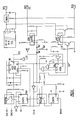
- FIG. 1 there is a peripheral unit (100) of actual capture and a central unit (200) for recording and control, these two units being interconnected by a line (300) of connection.
- the peripheral unit (100) is connected to the organism examined by a ground connection (400) and several pairs of measurement electrodes (500 and 600) forming the different measurement channels.
- the signal from each channel, picked up by a pair of electrodes (500 and 600), passes through a conditioning circuit (7) before reaching the differential and sequential sampling circuit (8).
- the sampling circuits (8) are connected in star to the transmission circuit (9) of the peripheral unit (100) for the measurement signals (AS) and are connected to each other by a circular connection (10) interrupted by an initialization circuit (11).
- the peripheral transmission circuit (9) is connected in star to the input (83) of the sampling circuits (8) and to the initialization circuit (11) for the control signal (CV).
- the peripheral transmission circuit (9) receives an event marking signal (EM) in addition to an identification signal (ID) coming from the initialization circuit (11).
- the output (99) of the peripheral transmission circuit (9), which constitutes the output of the peripheral unit (100), is linked by the connection line (300) to the input (211) of the central unit ( 200) recording which coincides with the input of the central transmission circuit (21) whose output (212) is connected to an interface (22) composed of address decoders and "latch" circuits so as to render the data directly accessible to a microprocessor at its "bus" (23).
- the conditioning circuit (7) includes an input protection (71) followed by a differential preamplifier (72) formed by two transistors (721 and 722) with field effects connected respectively to the electrodes (500 and 600).
- the "drain" (D) of each of these transistors (721 and 722) is respectively connected to identical resistors (731 and 732), themselves connected to an adjustment circuit (75) of the zero level.
- the outputs of the field effect transistors (721 and 722) of this preamplifier (72) are connected on the one hand to the inputs of the operational amplifier (761) and on the other hand respectively via the buffer amplifiers (771 and 772) and averaging resistors (773 and 774) at the positive input of the second operational amplifier (762), which in this way receives the average level of the potential present at the outputs of the field effect transistors (721 and 722) , while the negative input of this second operational amplifier (762) receives the average level of the potential present respectively at the positive and negative terminals of the power supply via the respective resistors (775 and 776).
- the outputs of the operational amplifiers (761 and 762) are connected via a voltage shift circuit (respectively 791 and 792) in a feedback loop to the current sources (741 and 742).
- the voltage offset circuits (791 and 792) are made up, in the example described according to the invention, of a simple resistor forming with the resistors (743 and 744) a divider bridge capable of adjusting the collector current of the transistors (745 and 746), at a value corresponding to the optimum source current operating point of the field effect transistors (721 and 722). This optimum operating point depends on the applications of the apparatus according to the invention, and perhaps, for example, the point of the zero temperature coefficient for the field effect transistors (721 and 722).
- each channel is therefore made up by a symmetrical differential circuit comprising an amplifier element with high input impedance, the field effect transistors (721 and 722), for each of the two inputs.
- the operating level, or reference voltage of each of said amplifier elements is controlled by a different feedback loop for each of them.
- the field effect transistor (722) this loop is controlled by the amplitude of the differential signal, coming from the operational amplifier (761), while the other (721) is controlled by the voltage common mode, coming from the operational amplifier (762).
- This double feedback loop maintains said amplifier elements at a relatively constant and perfectly symmetrical level of operation.
- a signal in the method according to the invention of multichannel capture for the digital recording of slow electrophysiological signals of low amplitude appears at one of the measurement electrodes (500 and 600), the potential difference transmitted to the first operational amplifier (761) will cause a negative feedback change in field effect transistor source current (722).
- the same potential modification will require, via the second operational amplifier (762), a modification of opposite direction at the level of the other field effect transistor (721). Consequently, the current in the two field effect transistors (721 and 722) will be maintained near the starting level.
- the small modification that remains in each of them will be symmetrical with respect to this operating point.
- the signals leaving the operational amplifiers (761 and 762) will be very large and may even reach satura tion in an attempt to control the current in the field effect transistors (721 and 722).
- these signals leaving the operational amplifiers (761 and 762), are used to indicate that such anomalies occur at the electrodes (500 and 600).
- the signals are compared in analog comparators (respectively 121 or 122) actuating a horn or an indicator (123 or 124) depending on whether the signal comes from the operational amplifier (762 or 761), each time this signal is too high.
- warning signals can be brought together by a door - or - into a single alarm per channel, or into a single alarm for all channels while activating a decoder with a digital display indicating the channel or electrode in question.
- These displays can be done at the peripheral unit or transmitted to the central unit in the form of an event marking signal, described below.
- the signal from the second operational amplifier (762) represents a common mode level.
- the signal from the first operational amplifier (761) contains the same common mode signal and the amplified electrode signal.
- a third amplifier (78) gives the difference between these two signals, the amplified electrode signal.
- the conditioning circuit (7) ends with a low pass filter (793) essentially intended to avoid errors of the "aliasing" type during the analog-digital conversion which will follow.
- the type of this filter and the cutoff frequency will depend on the smallest fre sampling frequency which is provided so as not to allow any significant component of the signal to persist at a frequency equal to or greater than half of this sampling frequency.
- the differential and sequential sampling circuit (8) (fig. 1 and 3) contains a first circuit (811) of the "sampling and holding” type, the input of which is connected to the output of the low-pass filter (793) ( Fig. 2 and 3) and whose output is connected to the negative input of the differential amplifier (841), Figure 3.
- a second circuit (812) of the "sampling and holding” type is mounted in feedback to the input positive of said differential amplifier (841).
- the output of said differential amplifier (841) passes, after additional amplification in the amplifier (842), to a switch (85) controlled by a logic circuit (86) before reaching the output (82) of the channel considered: the signal (AS).
- Said logic circuit (86) also controls the two circuits of the “sampling and holding” type (811 and 812).
- the outlet (82) of the channel in question, fig. 1 is connected in star form, with respect to the outputs (82) of the other channels, to the peripheral transmission circuit (9) which contains an analog-digital converter, described below, which performs the conversion of the analog samples coming from the outputs (82 ) in digital samples.
- each channel has in turn at its output (82) a potential, the signal (AS), the amplitude of which corresponds to the difference between the potential of the signal recorded during of a given analog-to-digital conversion and the potential of the same signal during the previous conversion of the same channel.
- AS the signal
- differential and sequential (8) Figure 3.
- This logic circuit (86) is mainly controlled by two flip-flop circuits (861 and 862).
- the first flip-flop circuit (861) is returned to its initial state on ignition by a "reset" signal (RT) produced for example by an RC circuit connected to the power supply.
- RT "reset" signal
- the input (83) receives a conversion signal (CV) common to all the channels and connected to the trigger input (CLK).
- the data input (D) of the first flip-flop circuit (861) of each channel is connected to the output (0) of the first flip-flop circuit (861) of the previous channel.
- This connection materializes the circular connection (10, fig. 1 and 3) between the channels.
- a channel is active when, and only when, the output (O) of its first flip-flop circuit (861) is active and closes the switch (85).
- This output (0) becomes active during the rising edge of said conversion signal (CV) if the data input (D), and therefore the output (O) of the first flip-flop circuit (861) of the previous channel, was active.
- the output (O) of the first flip-flop circuit (861) places the first "sampling and holding” type circuit (811) in its “holding” state by opening its switch (871). This active output (O) will trigger the first flip-flop circuit (861) of the next channel and the next differential and sequential sampling circuit (8) will therefore be activated on the next conversion while the currently active channel will no longer be.
- the falling edge of the conversion signal (CV) will trigger the second flip-flop circuit (862) by activating its input (CLK).
- Said second flip-flop circuit (862) controls the second "sampling and holding” type circuit (812) and puts it with its active output (O) in its "sampling” state by closing its switch (872).
- the second “sample and hold” type circuit (812) performs therefore a sampling while the first (811) is in the "hold” position. In this way, the output of the differential amplifier (841) goes to zero.
- the zero detector circuit (88) returns the second flip-flop circuit (862) to its initial state by its input (RST).
- the output (O) of the first flip-flop circuit (861) becomes inactive and the switch (85) is open so that only the sampling circuit (8 ) next is connected to the line of the signal to be converted (AS).
- the “sampling and holding” type circuit (811) regains its sampling state, and, gradually, any difference in the system input potential compared to the state during the last sampling appears amplified at differential amplifier output (841). This difference will be the subject of a new digital conversion at the next activation of the said channel.
- the output of the differential amplifier (841) When the output of the differential amplifier (841) is brought to zero, the signal at the output of the "sampling and holding" circuits (811 and 812) are identical as long as the four resistors controlling the differential amplifier (841) are identical. If this is not the case, the output of the differential amplifier (841) is canceled for values of the outputs of the circuits (811 and 812) which can be calculated according to the theory of operational amplifiers.
- the resistors (891 and 892) avoid oscillations during reset. However, they must be small enough for zero to be reached between the end of the conversion and the end of the main time. of the circuit (811).
- the effective value of the resistors (893 and 894) will be worth the real value of the resistance multiplied by a factor n / n-1.
- the initialization circuit (11), figure 3, is inserted in the circular connection (10) between the differential and sequential sampling circuits (8) (fig. 1) by its input (111) and its output (112) . It essentially contains a rocker circuit (113) which, unlike the rocker circuits (861) of the sampling circuits (8), is activated by the common "reset" pulse (RT) at the time of ignition. A first control pulse can thus be inserted into the circular connection (10) through the door - or - (114). Upon the first conversion signal (CV), the flip-flop circuit (113) is definitively deactivated. An output (115) allows, with a signal (ID), to indicate the moment when, after a full turn of the circular connection (10), and therefore of all the channels, the cycle will start again.
- a signal (ID) to indicate the moment when, after a full turn of the circular connection (10), and therefore of all the channels, the cycle will start again.
- the signal (ID) (fig.1) is therefore activated when the channel which precedes the initialization circuit (11) is active.
- One of the channels therefore provides an active signal (ID) when the corresponding channel is active, which will subsequently make it possible to identify this channel in the sequential transmission of signals from the different channels to the central unit (200, fig. 1).
- the conversion signal (CV) is directed to the differential and sequential sampling circuit (8) of all the channels and to the initialization circuit (11).
- the signal (AS) coming from the differential and sequential sampling circuit (8) of all the channels converging in star is directed like the signal (ID) coming from the initialization circuit (11) and the signal (EM) of marking d event towards the entrance to the cir peripheral transmission cooked (9), figure 1.
- Said peripheral transmission circuit (9), FIG. 4, mainly contains an analog-digital converter (91) with serial output (912), a time counter circuit (93), a digital multiplexer (94), a conditioning (96), and an isolation circuit (92) which connects the peripheral transmission circuit (9) with the central unit (200) via a connecting line (300).
- Said isolation circuit (92) comprising an optocoupler or other isolation element, receives clock pulses from the central unit (200). These are organized by pulse trains (CK) whose pulse frequency corresponds to the transmission speed and whose repetition frequency corresponds to the analog-digital conversion frequency. These pulse trains (CK) are transmitted to the input (931) sensitive to the falling edge of the time counter circuit (93). The first pulse of the train, finding the output (932) in the high state produces a reset to the initial state of the time counter circuit (93) thanks to the gate - and - (933) with the signal (XL) indicating the length of a clock pulse train.
- CK pulse trains
- the time counter circuit (93) controls the analog-digital converter (91) using the pulse trains (CK) to form the control signals (E and CLK), of which (E) is the activation signal and (CLK) is the clock signal; and supplies to another output the conversion signal (CV) and the signal corresponding to the complete cycle (FB) of the first clock times which are used to control the digital multiplexer (94).
- the input (941) of said digital multiplexer (94) is connected to the output (912) of the analog-digital converter (91), and its input (942) to the output (115) of the initialization circuit (11, Fig. 3) for the signal (ID) and its input (934) to the conditioning circuit (96) which receives the event marking signal (EM).
- the digital multiplexer (94) presents at its output (944) the identification signal (ID) during the first clock cycle and the serial output of the analog to digital converter (91), providing a sample of the converted channel, during the other cycles of the pulse train.
- the output (944) is connected to the signal (EM) conditioned by the conditioning circuit (96).
- the output (944) of said digital multiplexer (94) is connected to a door -and- (97) open only when the clock signal coming from the central unit (200) is inactive.
- the output of said gate -and- (97) is connected to the input of the transmission transmitter of the peripheral unit, included in the isolation circuit (92).
- the signal (DX) formed by the digital multiplexer (94) is therefore transmitted after isolation by optocoupler, or other isolation system in the circuit (92), to the central unit (200) at a rate of one bit during each inactive phase between the clock pulses.
- the end of a conversion signal (CV) blocks the reception of the pulse trains thanks to the refractory circuit (95) which makes it possible to synchronize the central unit (200) and the peripheral unit (100).
- the time constant of the refractory circuit (95) must be greater than one bell cycle to allow progressive synchronization. This synchronization takes place from the first sampling if the time constant is greater than the duration of a train of pulses.
- the communication circuit between the peripheral unit (100) and the central unit (200) comprises a transmitter circuit and a receiver circuit at the peripheral unit (100) forming part of the isolation circuit (92) and a another transmitter circuit as well as another receiver circuit at the level of the central unit (200) and forming part of the link circuit (31).
- the peripheral transmission circuit (9) cannot activate the reception circuit of said peripheral unit (100). This condition can be fulfilled for example by alternately inhibiting the circuit transmitter and the peripheral receiver circuit by a very high frequency oscillation in relation to the bell pulses.
- the receiver circuits must include a detector and a filter making it possible to find the clock and data pulses. Said high frequency can be generated by the oscillator of the transmitting circuit and the detection can be of the synchronous type.
- the central unit receiver circuit (200) is inhibited during the active phase of the clock pulses.
- a single line can therefore be used to transmit the clock pulses from the central unit (200) to the peripheral unit (100) and on the other hand, interleaved between the clock pulses, the data of the peripheral unit (100) to the central unit (200).
- Said transmission line can be constituted by an infrared system, an ultrasonic system or an electromagnetic system if the peripheral unit has its own power supply.
- Said very high frequency oscillation used to alternately inhibit the transmitter circuit and the peripheral receiver circuit can be used to generate ultrasound or electromagnetic waves.
- Said very high frequency oscillation and said own power supply are useless when a cable with three conductors, used as a connecting line (300), connects the peripheral unit (100) and the central unit (200).
- One of the three conductors constitutes the ground and can constitute the shielding of the cable.
- the second conductor constitutes the signl (DL) transmission line proper.
- the third conductor carries a supply current and is connected to the primary of the isolated DC / DC converter (98).
- the data is separated from the clock pulses by a gate (321) whose output can only be activated by the transmitted data during the inactive phase of the clock signal (CK).
- the first rising edge of the data pulses in positive logic or the falling edge in negative logic triggers the flip-flop circuit (33), which is reset to zero by each clock pulse (CK) through the gate (322) and between the clock pulse trains. Said triggering on the side of the data makes it possible to avoid the synchronization difficulties caused by transmission delays.
- the output (331) of the flip-flop circuit (33) which represents the serial data, is connected to the input (341) of the shift register (34) which performs the transformation of the serial data in parallel.
- the length of said shift register (34) must count as many bits as the length of the digital conversion words of the analog-digital converter (91), increased by one bit (the first) for the transmission of the channel indicator signal ( ID).
- the clock signal (CK) also controls the advancement of data in said shift register (34).
- the same pulse (CK) loads the output (331) of said rocker circuit (33) into said shift register (34) and on the other hand, resets the output (331) of said rocker circuit (33) ).
- a delay element like the delay circuit (35), is therefore essential between the output (331) of said rocker circuit (33) and the input (341) of said shift register (34) to avoid conflicts. of time.
- Figure 7 presents two alternative circuits (190 and 195) for the parallelization of the data which make it possible to avoid the delay circuit (35, fig. 4).
- These two circuits (190 and 195) are always preceded by the rocker circuit (33) triggered by the first side of the data as in the first example. This time, however, the flip-flop circuit (33) is no longer reset to zero at each bell signal but it is mounted as a frequency divider by two.
- the initial data are then reconstituted by doors -or exclusive- (191) to the shift register outputs (189) in the circuit (190), either by a second rocker circuit (193) and a single -or exclusive- gate (194) between the rocker circuit (33) and the register input shift (189) in the circuit (195).
- the 9-bit shift register is actually made up of a flip-flop circuit (188) followed by an 8-bit shift register (189).
- the door (323), FIG. 4, makes it possible to isolate the event marker signal (EM) present only between the pulse trains.
- the time controller circuit (36) is similar to that (93) of the peripheral transmission circuit (9) of the peripheral unit (100). From a continuous clock signal (BC) defining the transmission speed, and from a sampling signal (SC) determining the sampling rate, this time counter circuit (36) generates the trains of clock pulses (CK) transmitted to the peripheral unit (100) and controlling said shift register (34). Said time counter circuit (36) also provides an active signal (DR) between said clock pulse trains (CK) and transmitted to the interface (22) to indicate that the data of the shift register (34 ) are available. Said time counter circuit (36) provides a third signal (DG) active during periods when no normal data is transmitted. The door (323) opened by said third signal (DG) makes it possible to collect any event marking pulse (EM) transmitted by the peripheral unit (100) outside of the normal transmission times.
- BC continuous clock signal
- SC sampling signal
- the event marker signal can respond to numerous applications in the context of the present invention.
- the transmitted signal can be a modulated signal or a simple all-or-nothing marker.
- the message can relate to a particular state of the peripheral unit (100) such as for example an unacceptable condition at the input as revealed by the analog comparator (121 and 122, fig. 2).
- the signal can also represent a message from the organism studied.
- the event marker signal can very well provide the response to stimulation of an examined subject while the electrodes of the various measurement channels record the electroen cephalogram.
- a different event marker signal can be generated for each input channel. These signals are then gathered on a single line thanks to a logic gate opened by and during the duration of the signal of the corresponding channel in the circular connection (10, fig. 3). A time multiplexing is thus carried out and the decoding is done in the central unit (200) by the relationship between the identification pulse (ID) and the time of appearance of an event marker corresponding to a given channel.
- ID identification pulse
- the generator circuit (361), fig. 4, can produce the continuous clock signal (BC), which represents the base frequency, from a clean oscillator or by means of frequency dividers from a general clock.
- the circuit (362), which provides the sampling signal (SC) determining the sampling rate, can also vary depending on the applications.
- an oscillator constructed using a "phase locked loop" circuit and a frequency divider makes it possible to synchronize a faster sampling speed with the slower sector frequency. Such synchronization makes it possible in certain situations to limit interference from the mains when recording signals of low amplitude.
- the microprocessor interface (22) must be constructed according to the requirements of the microprocessor used. In its simplest version, it includes buffer registers making the data accessible directly on the "bus" (23) of the microprocessor thanks to an address decoder.
- the data received by the microprocessor represent for each channel the successive differences between the signal level at the time of two consecutive sampling times.
- the starting level of the signal therefore remains unknown, which has no importance in the field of application provided for the example of the figures (1 to 8).
- the base potential superimposed on the signal can sometimes be subject to slow variations called drift.
- the influence of temperature and other changes in the electronic input circuit can also add a technical component to this drift. Any constant error in the differential signal will also appear when reconstructing an undifferentiated signal as a drift.
- the microprocessor removes from each data item received a coefficient intended to compensate for all sources of drift.
- this correction coefficient X is estimated, which is represented in box 1 of FIG. 8, by selecting two consecutive differential samples S (i) whose absolute value of their difference is less than a predetermined value d and by equalizing this coefficient X to one differential sample S (i).
- the value d is therefore a difference initially admitted between two samples.
- the adjustments are made using an estimate for N successive samples. N is therefore the number of samples included in the evolution of the drift.
- the total drift Y over these N samples is estimated to be equal to N x X.
- the level of the signal L (i) is initialized to an arbitrary value ⁇ .
- FIG. 5 shows the time relationships of the various signals of the apparatus according to the invention.
- the central unit there is the continuous clock signal (BC) produced by the generator circuit (361, fig. 4), the sampling signal (SC) supplied by the circuit (362).
- the time counter (36) From these signals (BC) and (SC) the time counter (36) generates the signal (DR) transmitted to the interface (22) and active between the clock pulse trains (CK), the signal (DG ) also active between the clock pulse trains (CK) and activating inter alia the gate (323), and the third signal representing the said clock pulse trains (CK) transmitted to the peripheral unit (100 ) and transmitted to the input (931) of the peripheral time counter circuit (93).
- the signal (DS) represents a sample paralleled by the shift register (34).
- the signal (DL) is that which is transmitted between the central unit (200) and the peripheral unit (100) on one of the conductors of the connection line (300).
- a signal (XL) which indicates the length of a train of clock pulses (CK) coming from the central unit (200) and which resets the time counter circuit. (93) in the initial state.
- the time counter circuit (93) supplies the signal (FB) which corresponds to a complete cycle of the first clock time and which is used to control the digital multiplexer and the conversion signal (CV, fig. 4 & 3).
- the signal (DX) formed by the digital multiplexer (94) is transmitted to the central unit (200). Note that some analog-to-digital converters (91) require a certain number of initial clock pulses before starting the actual conversion. These additional cycles are shown in dotted lines (3, fig. 5).
- FIGS. 6 and 7 represent an exemplary embodiment of a two-channel system (CH1 and CH2) making it possible to simplify the control of the succession of channels carried out by a single flip-flop circuit (109) in place of a circuit with flip-flop (861, fig. 4) for each channel and the flip-flop circuit (113, fig. 4).
- FIG. 6 also represents the time counter circuit (116) and the analog-digital converter (134), (respectively 93 and 91 of FIG. 4). Transmission is ensured by two optocouplers (139 and 147) mounted in such a way that they share the same connection line (162) without, however, the output of the optocoupler (147) being able to influence the input of the optocoupler. (139).
- the refractory circuit (95, fig. 4) is formed by the capacitor (140), the diode (141) and the resistor (142).
- the transmission is controlled by the transistors (169 and 171), controlled by the transistor (175), which transmit the clock pulses in the form of current increments which must activate the optocoupler (139, fig. 6).
- the blocking door (321, fig. 4) is represented by the transistor (178) and the resistor (173).
- the capacitor (180) adds a filter element and the transistor (182) acts as a buffer for the inverter (184).
- the LED diode (165) makes it possible to observe at the level of the central unit that the peripheral unit is well connected and that the fuse (164) is still in good condition.
- the time counter circuit (36, fig. 4) is here represented by the circuit (198) and the doors which accompany it as well as the rocking circuit (203).
- connection (300, fig. 4) between the central unit (200, fig. 4) and the peripheral unit (100, fig. 1) comprises the supply wires (161 and 163) , of which the conductor (163) is the mass, as well as the transmission line (162).
- This connection could be replaced by a battery at the peripheral unit and an infrared, ultrasonic or electromagnetic transceiver pair at each end of the line (162) which would be removed.
- On the side of the peripheral unit it is essential to add a very high frequency oscillator, possibly common to the transmission generator and capable of alternately inhibiting the transmitter and the peripheral receiver, in order to prevent them from interfere with each other.
- the two receivers of the system are provided with a detector, possibly of the synchronous type, and with a filter capable of eliminating the high frequency modulation thus introduced in order to recover the initial signal.
- the planned transmission schemes could very well in the context of the present invention, include an error detection system such as a parity bit. This However, this kind of precaution is not very common in biology where a more effective solution to improve the reliability of the apparatus consists in taking more samples than the minimum necessary.
- FIG. 9 Another exemplary embodiment of the present invention can be described with the aid of FIG. 9.
- This figure can be compared to FIG. 3. It comprises a branch circuit (6) in which a flip-flop initialization circuit ( 64) be inserted by connections (66) and (67) in a circular connection as described in Figure 1 under the number (10) and here called primary loop (10), as opposed to the secondary loop (10 ⁇ ) connected in (61) and (62).
- the bypass element (6) directs a sampling pulse (CV) to the initialization flip-flop circuit (65) of the secondary loop (10 ⁇ ).
- the sampling pulses thus obtained are called (CV2).
- the sampling speed in the secondary loop (10 ⁇ ) will therefore be much slower than in the primary loop (10) since only one channel of the secondary loop (10 ⁇ ) will be successively activated by the system at each turn of the primary loop. (10).
- Several secondary loops (10 ⁇ ) can be inserted and the number of channels of the primary (10) and secondary (10 ⁇ ) loops can be chosen so as to obtain the desired sampling frequency ratio for each channel.
- the primary loop (10) transmits an identification bit (ID) when the first channel is activated; similarly, each secondary loop (10 ⁇ ) transmits a bit (ID2) corresponding to its first channel. It is obvious that longer words will be required during transmission in order to include the additional "bits” thus created.
- the different identification signals of the first bit can each be also linked to a frequency multiplier (63) so as to provide a control signal for the filters. to "switched capacity". In the example given, the frequency (F2) is obtained from (ID2) and (F1) from (ID). This latter link has not been shown.
- Such an arrangement has the advantage of seeing the cut-off frequency of the low-pass filters (51) adapt to the sampling frequency without requiring modification of the circuits of the peripheral unit (100).
- the central unit (200) can therefore modify the sampling frequencies without fear of introducing "aliasing" errors.
- FIG. 9 also includes an example of a sampling circuit which is a little different from what is shown in FIG. 3.
- the sampling circuit (5) contains three channels. The first, having as input (50) the output of the amplifier (78) of FIG. 2 and therefore receiving the amplified electrode signal, is inserted into the primary loop (10). The other two channels are inserted in a secondary loop (10 ⁇ ). Each of the three channels is controlled by a flip-flop circuit (50) controlled by the conversion signal (CV) for the primary loop channel (10) and by the conversion signal (CV2) for the secondary loop channels ( 10 ⁇ ).
- CV conversion signal
- CV2 conversion signal
- the sampling system (53) comprises two identical "sampler and hold" circuits (531) which are activated alternately by a flip-flop circuit (58) so that their output signal corresponds respectively to the signal value at the current sampling time and at the previous sampling time.
- a flip-flop circuit 58
- the outputs of the sampling system (53) are connected to a differential amplifier (57). The latter provides the successive differences comparable to those obtained in the circuit of FIG. 3.
- the circuit of FIG. 9 is also distinguished by the comparator (52).
- This comparator (52) opens the switches of the sampling system (53) as soon as the signal exceeds the positive reference (R +) or becomes lower than the negative reference (R-) used by the analog-digital converter. This opening results in more severe low-pass filtering by the sampling system (53) itself; thus, no long-term error will be caused by a signal whose slope is momentarily too fast.
- the output of the comparator (52) is also connected to a circuit (55) forming a function "or" wired with the circuits similar to other channels so that a signal (OV) transmitted to the central unit (200) allows the latter to react with an appropriate indication and, or, by modifying the sampling speed.
- the direct signal as it enters the sampling system (53) is transmitted after appropriate amplification and filtering by one of the channels of the secondary loop (10 ⁇ ).
- the shaping circuits are classic.
- the filtering can be carried out as indicated in FIG. 9 by means of a "switched capacity" filter (51) controlled by the frequency (F2).
- the second channel of the secondary loop (10 ⁇ ) is identical except its input (56) which is connected to the output of the amplifier (762, Figure 2). This output provides a signal proportional to the common mode voltage if the dividing bridges (791), (743) and (792), (744) in Figure 2 have been correctly adjusted.
- the triple path of the circuit (5) of FIG. 9 it is possible to transmit to the central unit (200) the amplitude of the common mode potential, the amplitude of the direct signal and the successive differences in amplitude. of the signal.
- This last value is strongly amplified and can by successive summations reconstruct the input signal with a very large dynamic range. Errors introduce a drift which must be the subject of a simple correction (figure 8) or more complex for example by modifying the values of d (figure 8) or by using the statistical calculation of a regression line by the formula least squares.
- the central unit (200) receives the value of the direct signal transmitted with a much smaller amplification and possibly with a much slower rhythm than the differences, it is possible to use this value to compare it with the result of the successive summations differences. Any error of the sum equivalent to the least significant bit of the direct signal may cause the object of a new estimation of the correction to be applied to the samples of the differences so as to eliminate the observed drift. When the corrections applied approach an ideal value, this type of correction will occur more rarely since the successive sums will give an image of higher resolution and a content richer in frequency but of identical value to the direct signal.
- the value of the common mode potential also transmitted to the central unit (200) gives access to the information concerning the input circuit. This information can be displayed or recorded at the level of the central unit (200).
- the signals (ID) can be used by the central unit not only to identify the activated channel but also to automatically calculate the number of channels installed in the peripheral unit and check their interrogation successively thanks to a counter of the samples transmitted between two signals (ID).
- ID2 can be used by the central unit not only to identify the activated channel but also to automatically calculate the number of channels installed in the peripheral unit and check their interrogation successively thanks to a counter of the samples transmitted between two signals (ID).
- ID2 can be used by the central unit not only to identify the activated channel but also to automatically calculate the number of channels installed in the peripheral unit and check their interrogation successively thanks to a counter of the samples transmitted between two signals (ID).
- ID2 The same system can be applied to (ID2).
- the central unit (200) can also trigger different states of the peripheral unit (100) by sending additional clock pulses in the pulse trains.
- the peripheral unit (100) has a refractory circuit (95), ( Figure 4) limiting the number of pulses normally present in each train.
- a refractory circuit could moreover be produced by means of a frequency multiplier supplied by the conversion pulses (CV) and connected to a counter.
- Any clock pulse received during the refractory period can be derived towards a control circuit capable of activating different states of the peripheral unit (100) such as for example different gains of the amplifiers or different cutoff frequencies of the filters.
- the triggering by one of its states, of a conventional system of calibration and measurement of electrode impedances is a possi bility.
- Another state can induce a signal (RT) and thus cause a return of all the loops to their initial state.
- Another possible application is the triggering of accessories external to the system.
- Another particular state of the peripheral unit (100) could consist in raising the connection of the ground electrode (400, figure 1) by a small known value of potential with respect to the ground of the input circuit. The values of common mode potential and of the signal obtained during this operation make it possible to directly check the correct operation of all the input circuits and in particular their capacity for rejection of the common mode potential.
- the transmission circuit is not different from what is shown in FIG. 4.
- the circuits (93) and (94 ) in particular must be adapted to the analog-digital converter and to the organization of the different channel loops.
- Several combinations of counters and logic gates and, or, a microcontroller and, or, memory of PROM or EPROM tupes and, or, PLA circuits can find their application here.
- control signals CK and DR as well as the output of the flip-flop (188) or (193) of FIG. 7, according to the desired code, can supply a serial output when such an output is required.
- the signal samples are digitized in 8 bit. Depending on the application, this number of bits may be different.
- circuits of the present invention can be produced in several classes of circuits such as bipolar, CMOS, HCMOS, HCTMOS or others.
- organization of the apparatus can in the context of the present invention be divided into essential parts or standardized modules which can be produced on microchips for example. The construction of an apparatus adapted to a particular application then amounts to simply assembling the necessary modules.
Landscapes
- Health & Medical Sciences (AREA)
- Life Sciences & Earth Sciences (AREA)
- Engineering & Computer Science (AREA)
- Pathology (AREA)
- Heart & Thoracic Surgery (AREA)
- Physics & Mathematics (AREA)
- Veterinary Medicine (AREA)
- Biophysics (AREA)
- Public Health (AREA)
- Biomedical Technology (AREA)
- Computer Networks & Wireless Communication (AREA)
- Medical Informatics (AREA)
- Molecular Biology (AREA)
- Surgery (AREA)
- Animal Behavior & Ethology (AREA)
- General Health & Medical Sciences (AREA)
- Power Engineering (AREA)
- Physiology (AREA)
- Measurement And Recording Of Electrical Phenomena And Electrical Characteristics Of The Living Body (AREA)
Applications Claiming Priority (2)
| Application Number | Priority Date | Filing Date | Title |
|---|---|---|---|
| BE216706 | 1986-05-27 | ||
| BE0/216706A BE904825A (fr) | 1986-05-27 | 1986-05-27 | Methode et appareillage de captation multicanal pour l'enregistrement digital de signaux electrophysiologiques lents et de fiable amplitude. |
Publications (1)
| Publication Number | Publication Date |
|---|---|
| EP0247991A1 true EP0247991A1 (de) | 1987-12-02 |
Family
ID=3844038
Family Applications (1)
| Application Number | Title | Priority Date | Filing Date |
|---|---|---|---|
| EP87870074A Withdrawn EP0247991A1 (de) | 1986-05-27 | 1987-05-22 | Verfahren und Gerät zur mehrkanaligen Messung und digitalen Registrierung von niederfrequenten physiologischen Signalen geringer Amplitude |
Country Status (2)
| Country | Link |
|---|---|
| EP (1) | EP0247991A1 (de) |
| BE (1) | BE904825A (de) |
Cited By (2)
| Publication number | Priority date | Publication date | Assignee | Title |
|---|---|---|---|---|
| EP1050270A1 (de) * | 1999-05-07 | 2000-11-08 | Bruker Medical SA | Verfahren und Vorrichtung zur Erfassung von Elektrokardiogrammen |
| CN111132612A (zh) * | 2017-09-26 | 2020-05-08 | 诺基亚技术有限公司 | 用于感测生物信号的设备 |
Families Citing this family (1)
| Publication number | Priority date | Publication date | Assignee | Title |
|---|---|---|---|---|
| US5368041A (en) * | 1992-10-15 | 1994-11-29 | Aspect Medical Systems, Inc. | Monitor and method for acquiring and processing electrical signals relating to bodily functions |
Citations (6)
| Publication number | Priority date | Publication date | Assignee | Title |
|---|---|---|---|---|
| US3757778A (en) * | 1971-01-13 | 1973-09-11 | Comprehensive Health Testing L | Electrocardiograph lead distribution and contact testing apparatus |
| US3885552A (en) * | 1972-11-16 | 1975-05-27 | Pacemaker Diagnostic Clinic Of | Cardiac function monitoring system and method for use in association with cardiac pacer apparatus |
| US3910257A (en) * | 1973-04-25 | 1975-10-07 | Nasa | Medical subject monitoring systems |
| GB2003276A (en) * | 1977-08-29 | 1979-03-07 | Karz A | Continuous electrocardiogram monitoring method and system for cardiac patients |
| DE2816494A1 (de) * | 1978-04-15 | 1979-10-25 | Collectron System Ag | Geraet zum erfassen physiologischer messwerte |
| EP0161154A1 (de) * | 1984-04-06 | 1985-11-13 | STMicroelectronics S.A. | Breitbandverstärker mit doppelter Gleichtaktgegenkopplung |
-
1986
- 1986-05-27 BE BE0/216706A patent/BE904825A/fr not_active IP Right Cessation
-
1987
- 1987-05-22 EP EP87870074A patent/EP0247991A1/de not_active Withdrawn
Patent Citations (6)
| Publication number | Priority date | Publication date | Assignee | Title |
|---|---|---|---|---|
| US3757778A (en) * | 1971-01-13 | 1973-09-11 | Comprehensive Health Testing L | Electrocardiograph lead distribution and contact testing apparatus |
| US3885552A (en) * | 1972-11-16 | 1975-05-27 | Pacemaker Diagnostic Clinic Of | Cardiac function monitoring system and method for use in association with cardiac pacer apparatus |
| US3910257A (en) * | 1973-04-25 | 1975-10-07 | Nasa | Medical subject monitoring systems |
| GB2003276A (en) * | 1977-08-29 | 1979-03-07 | Karz A | Continuous electrocardiogram monitoring method and system for cardiac patients |
| DE2816494A1 (de) * | 1978-04-15 | 1979-10-25 | Collectron System Ag | Geraet zum erfassen physiologischer messwerte |
| EP0161154A1 (de) * | 1984-04-06 | 1985-11-13 | STMicroelectronics S.A. | Breitbandverstärker mit doppelter Gleichtaktgegenkopplung |
Cited By (5)
| Publication number | Priority date | Publication date | Assignee | Title |
|---|---|---|---|---|
| EP1050270A1 (de) * | 1999-05-07 | 2000-11-08 | Bruker Medical SA | Verfahren und Vorrichtung zur Erfassung von Elektrokardiogrammen |
| FR2793131A1 (fr) * | 1999-05-07 | 2000-11-10 | Bruker Medical Sa | Procede et dispositif pour l'acquisition de l'electrocardiogramme |
| US6873869B2 (en) | 1999-05-07 | 2005-03-29 | Schiller Medical | Method and apparatus for obtaining an electrocardiograph |
| CN111132612A (zh) * | 2017-09-26 | 2020-05-08 | 诺基亚技术有限公司 | 用于感测生物信号的设备 |
| CN111132612B (zh) * | 2017-09-26 | 2023-06-30 | 诺基亚技术有限公司 | 用于感测生物信号的设备 |
Also Published As
| Publication number | Publication date |
|---|---|
| BE904825A (fr) | 1986-09-15 |
Similar Documents
| Publication | Publication Date | Title |
|---|---|---|
| EP0057802B1 (de) | Phasen- und Amplitudenmessung für ein Bohrlochsystem zur Bestimmung der dielektrischen Eigenschaften | |
| EP0586286B1 (de) | Drahtloses Übertragungssystem für medizinische Daten | |
| FR2485856A1 (fr) | Systeme d'acquisition de donnees et convertisseur analogique-numerique | |
| WO2010010278A1 (fr) | Transmission multicanaux sur un bus unifilaire | |
| EP0398824A1 (de) | Numerischer Isolationsprüfer für ein elektrisches Netz | |
| EP0279711B1 (de) | Verfahren und Vorrichtung zur Signalübertragung zwischen zwei Teilen | |
| EP0114544B1 (de) | Verfahren und Anordnung zur Fernsteuerung von Datensammlungsanlagen mittels eines Übertragungswegs mit schmalem Durchlassband | |
| FR2555383A1 (fr) | Dispositif de surveillance automatique de recepteurs radio ou television a fins d'etudes statistiques d'audience des differentes stations emettrices | |
| EP0094279B1 (de) | Verfahren zum Schutz eines Fernüberwachungssystemes gegen Sabotage und System zur Ausführung dieses Verfahrens | |
| FR2487143A1 (fr) | Boucle de mise a zero automatique a deux bandes passantes pour codeur-decodeur a frequence vocale | |
| EP0247991A1 (de) | Verfahren und Gerät zur mehrkanaligen Messung und digitalen Registrierung von niederfrequenten physiologischen Signalen geringer Amplitude | |
| FR2504329A1 (fr) | Recepteur multifrequence | |
| FR2465366A1 (fr) | Circuit de decalage de tension pour amplificateur a basse tension | |
| EP0393123A1 (de) | Elemente zur erregung und abtastung von am reifen befindlichen modulen in einem fahrzeugreifenüberwachungssystem. | |
| CA1263188A (fr) | Dispositif pour amplifier et echantillonner des signaux a grande dynamique | |
| EP0097753A1 (de) | Tonempfänger für digitales Datenübertragungssystem | |
| FR2581198A1 (fr) | Dispositif d'elimination des echos fixes d'un radar et radar comportant un tel dispositif. | |
| EP0866326B1 (de) | Installation zur Aufspürung und Ortung von Flüssigkeitsleckagen | |
| FR2598869A1 (fr) | Detecteur de phase et de frequence, et son utilisation dans une boucle a verrouillage de phase | |
| CA1293537C (fr) | Dispositif perfectionne pour l'echantillonnage de signaux | |
| FR2613079A1 (fr) | Appareil de test automatique de circuits electroniques et de mesure de temps | |
| FR2581196A1 (fr) | Procede et dispositif de mesure de resistivite, notamment pour liquides dielectriques de resistivite tres elevee. | |
| EP0336336A1 (de) | Schaltung zur Messung der Fehlerrate für ein synchrones digitales Übertragungssystem | |
| FR2559977A1 (fr) | Procede de mesure rapide du taux d'erreurs binaires d'un canal de transmission, et dispositif pour la mise en oeuvre de ce procede | |
| EP0843447A1 (de) | Verfahren zur Übertragung von asynchronen NRZ-Signalen mittels Frequenzmodulation |
Legal Events
| Date | Code | Title | Description |
|---|---|---|---|
| PUAI | Public reference made under article 153(3) epc to a published international application that has entered the european phase |
Free format text: ORIGINAL CODE: 0009012 |
|
| AK | Designated contracting states |
Kind code of ref document: A1 Designated state(s): AT BE CH DE ES FR GB IT LI NL SE |
|
| 17P | Request for examination filed |
Effective date: 19880519 |
|
| 17Q | First examination report despatched |
Effective date: 19910417 |
|
| STAA | Information on the status of an ep patent application or granted ep patent |
Free format text: STATUS: THE APPLICATION IS DEEMED TO BE WITHDRAWN |
|
| 18D | Application deemed to be withdrawn |
Effective date: 19910828 |
|
| RIN1 | Information on inventor provided before grant (corrected) |
Inventor name: DELBEKE, JEAN, DR. |