EP0248235A2 - Appareil de traitement d'image ayant fonction d'élargissement et/ou de réduction d'image - Google Patents
Appareil de traitement d'image ayant fonction d'élargissement et/ou de réduction d'image Download PDFInfo
- Publication number
- EP0248235A2 EP0248235A2 EP87106730A EP87106730A EP0248235A2 EP 0248235 A2 EP0248235 A2 EP 0248235A2 EP 87106730 A EP87106730 A EP 87106730A EP 87106730 A EP87106730 A EP 87106730A EP 0248235 A2 EP0248235 A2 EP 0248235A2
- Authority
- EP
- European Patent Office
- Prior art keywords
- bits
- data
- input
- pixcel
- shrinking
- Prior art date
- Legal status (The legal status is an assumption and is not a legal conclusion. Google has not performed a legal analysis and makes no representation as to the accuracy of the status listed.)
- Granted
Links
Images


Classifications
-
- G—PHYSICS
- G06—COMPUTING OR CALCULATING; COUNTING
- G06T—IMAGE DATA PROCESSING OR GENERATION, IN GENERAL
- G06T3/00—Geometric image transformations in the plane of the image
- G06T3/02—Affine transformations
Definitions
- This invention relates to an image processing apparatus having a function of enlarging and/of shrinking a somce image with an arbitary scale factor.
- NN Nearest Neighbour
- image data is processed word by word in general.
- processed bits must be packed word by word. This packing operation also requires a long period of time.
- An object of the present invention is to provide an image processing. apparatus which can perform enlarging operation and/or shrinking operation at a high speed' without executing complex calculation.
- An image processing apparatus of the present invention comprises means for receiving a plurality of original image data word by word, each data consisting of a fixed number of bits, an enlarging of shrinking circuit having a plurality of gating circuits each gating arbitrary bit or bits of the original image data according to a scale factor, a means for selecting one of the gating circuits in response to a signal representing a desired scale factor to open the selected gate, and means for outputting an image data which consists of bit or bits passing through the selected gating circuit.
- a mask circuit and a rotator may be used to perform a packing operation to pack the outputted image data into one word, if necessary.
- each gating circuit gates those bits which are same in number as those of the original image data and which contain two or more bits having the same content as one of the bits of the original image data.
- the gating circuits gate different numbers of bits less than the number of bits the original image data.
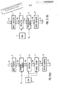
- an image processing apparatus has an input register 1, a shrinking circuit 2, an enlarging circuit 3, a mask circuit 4 having a temporary register, a rotator 5, an output register 6 and a read only memory ROM 7, all of which are coupled to a common bus 10.
- the shrinking circuit 2 works to shrink a source image and may be omitted if shrinking operation is not required.
- the enlarging circuit 3 may be omitted if enlargement is not required.
- the mask circuit 4, the rotator 5 and the ROM 7 are used to simplify the packing operation.
- one word consists of 8 bits (8 pixcel data).
- the pixcel data of the source image are entered into the input register 11 via a bus 11 word by word and an processed pixcel data are derived from the output register 6 to a bus 12 word by word.
- the source image usually consists of a plurality of words and is stored in a source memory (not shown).
- the source image is read out therefrom word by word.
- Each word consists of 8 bist of continous pixcel data in horizontal direction of XY co-ordinater and is entered into the input register 1 which has a capacity of 16 bits.
- a word to be shrinked is entered into the shrinking circuit 2 and thereafter a shrinked pixcel data is to the rotator 5 and the mask circuit 4 as shown in fig. 2(a).
- two consecutive words are entered into the input register 1 and sent therefrom to the rotator 5 and thereafter the rotated word is sent to the enlargement circuit 3 as shown in Fig. 2(b).
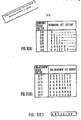
- the shrinking circuit 2 is formed of simple selecting circuits which are predetermined to pick up the bit or bits in accordance with the shrinking factors. If the shrinking scale factor is S is selected among seven factors 1/8, 2/8, 3/8, 4/8, 5/8, 6/8 and 7/8 and 8 bits pixcel data are represented by A B C D E F G H as shown in fig. 3(c), the bit or bits to be picked up are predetermined as shown in fig. 3(a).
- the pixcel data (word) of fig. 3(c) is sent to the shrinking circuit 2 via the common bus 10, and the shrinking circuit 2 has a selecting function to select one of the seven outputs shown in fig. 3(a) according to the shrinking scale factor S s .
- Each bit of the input register 1 is connected to the gate circuits 20 to 26 as shown in fig. 5.
- the decoder 27 When m is 1, the decoder 27 outputs a signal for the shrinking scale factor of 1/8 to activate or enable the gate circuit 20 only. Thus, the pixcel data A is picked up. When m is 2, the gate circuit 21 is selectively enabled and the pixcel data A and E are picked up. When m is 3, 4, 5, 6 or 7, the gate circuit 22, 23, 24, 25 or 26 is selected, respectively, and the pixcel data ADG, ACEG, ACDEFH, ABDEFH and ABCDFGH are picked up. As shown in fig. 5, the shrinking circuit 2 can be formed as a simple selector.
- the packing operation is executed by use of the rotator 5 and the masking circuit 4.
- the well known shiftregister having a feedback loop to return a shift out bit or bits to its input can be used as the rotator 5.
- a barrel shifter is suitable as the shiftregister.
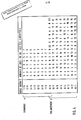
- a number of bits to be shifted is determined according to the shrinking scale factor as shown in fig. 4.
- m bits are picked up from 8 bits of a first one word as shown in fig. 3(a).
- the picked-up m bits are entered into the mask circuit 4 through the rotator 5. At this time the picked-up m bits are not shifted and are entered into 1st to mth bit positions of the mask circuit 4.
- the mask circuit 4 and the temporary register have 16-bit positions, . respectively, for the enlargement operation and 8-bit positions can only used in the shrinking operation.
- An output of the mask circuit 4 is set at 1st to 8th bit positions of the temporary register.
- 3 bits among 8-bits of a first word are picked up by the shrinking circuit 2. These 3 bits are not shifted and are entered into 1st to 3rd bit positions of the mask circuit 4.
- the mask circuit 4 masks the reminder 4th to 8th bit positions. Consequently, the 3 bits picked up from the first word are set into 1st to 3rd bit positions of the temporary register. Thereafter a second word subsequent to the first word is entered into the shrinking circuit 2 and 3 bits thereof are picked up. These subsequently shrinked 3 bits are shifted by 3 bit positions in the rotator 5 and entered into 4th to 6th bit positions of the mask circuit 4.
- the mask circuit 4 masks the bit positions (1st to 3rd and 7th to 8th) expect for the 4th to 6th bit positions.
- the 3 bits picked up from the second word are set into the 4th to 6th bit positions of the temporary register.
- a third word subsequent to the second word is entered into the shrinking circuit 2 and the picked up 3 bits are sent to the rotator 5 where they are shifted by 6 bits positions as indicated in fig. 4.
- First two of the shifted three bits are entered into the 7th and 8th vacant bit positions of the temporary register via the mask circuit 4 which masks the 1st to 6th bit position.
- 8 bit postions are filled up to form one word which corresponds to 3/8 - shrinked word and which is sent to the output register 6 and then to a destination memory (not shown) which is coupled to the bus 12.
- the last bit of the three bits out of the input third word is shifted out from the rotator 5 and is rotated to a first bit position of the rotator 4,
- the rotated last bit is thereafter entered into the 1st bit position of the mask circuit 4 and is set in the 1st bit position of the temporary register.
- a fourth word is applied to the shrinking circuit 2 through the input register 1 and 3 bits are picked up by the shrinking circuit 2.
- the picked up 3 bits from the fourth word are shifted by one bit in the rotator 5 as shown in fig.
- shrinking operation proceeds, and the shrinked pixcel data of 8 bits is packed word by word.
- m bits are picked up from each word by the shrinking circuit 2, shifted or rotated by the rotator 5 by the respective bits shown in fig. 4, and written into the temporary register from which the shrinked data is read 8 bits by 8 bits.
- Data shown in fig. 4 representing the number of bits to be shifted or rotated are stored in the ROM 7 and are read out thereof according to the scale factor m.
- a first word (8 bits) and a second word (8 bits) are entered into the input register 1 of the 16 bits.
- the rotator 5 of the -16 bits shifts the 16 bits of the first and second words by number of bits designated in fig. 4 in accordance with the scale factor.
- a start bit to be enlarged is located at the most significant bit (MSB) position.
- MSB most significant bit
- An output of the rotator 5 is sent to the enlarging circuit 3.
- the enlarging circuit 3 contains seven 8-bit gate circuits 30 to 36 which are coupled to the respective bit positions of the 8-bit input data lines of the circuit 3 such that the eight outputs from the first 8-bits of the input data shown in fig. 3(b) may be respectively derived therefrom.
- a A A B B B C C is derived from the enlarging circuit 3 as a first enlarged output for the original pixcel data and directly sent to the output register 6 through which this output is sent to the destination memory (not shown). Then, the same 16 - bit input data is shifted in the rotator 5 by m bits (in the above case, 3 bits) such that the (m-1)th (4th) bit locates at a first bit position.
- the rotator 5 performs shift operations by 2m bit (6 bits in the above case) and first eight bits G H A' B' C' D' E' F' of the 6-bit shifted input words are subjected to the enlarging operation by the enlarging circuit 3 to obtain a third output data G G G H H H A' A' through the gate circuit 32.
- a third word A" B" C" D" E” F" G" H" of 8 bits in the source image is newly entered into the input register 1 instead of the first word.
Landscapes
- Physics & Mathematics (AREA)
- General Physics & Mathematics (AREA)
- Engineering & Computer Science (AREA)
- Theoretical Computer Science (AREA)
- Image Processing (AREA)
- Digital Computer Display Output (AREA)
- Editing Of Facsimile Originals (AREA)
- Controls And Circuits For Display Device (AREA)
Applications Claiming Priority (2)
| Application Number | Priority Date | Filing Date | Title |
|---|---|---|---|
| JP105917/86 | 1986-05-08 | ||
| JP61105917A JPH0810462B2 (ja) | 1986-05-08 | 1986-05-08 | 画像処理装置 |
Publications (3)
| Publication Number | Publication Date |
|---|---|
| EP0248235A2 true EP0248235A2 (fr) | 1987-12-09 |
| EP0248235A3 EP0248235A3 (en) | 1989-08-09 |
| EP0248235B1 EP0248235B1 (fr) | 1994-03-09 |
Family
ID=14420215
Family Applications (1)
| Application Number | Title | Priority Date | Filing Date |
|---|---|---|---|
| EP87106730A Expired - Lifetime EP0248235B1 (fr) | 1986-05-08 | 1987-05-08 | Appareil de traitement d'image ayant fonction d'élargissement et/ou de réduction d'image |
Country Status (4)
| Country | Link |
|---|---|
| US (1) | US4907284A (fr) |
| EP (1) | EP0248235B1 (fr) |
| JP (1) | JPH0810462B2 (fr) |
| DE (1) | DE3789253T2 (fr) |
Cited By (2)
| Publication number | Priority date | Publication date | Assignee | Title |
|---|---|---|---|---|
| EP0497494A1 (fr) * | 1991-02-01 | 1992-08-05 | International Business Machines Corporation | Dispositif de cadrage d'image pour un système multimédia |
| EP0762325A3 (fr) * | 1995-08-31 | 1998-06-17 | General Instrument Corporation | Appareil d'agrandissement vidéo |
Families Citing this family (18)
| Publication number | Priority date | Publication date | Assignee | Title |
|---|---|---|---|---|
| JPH0751370B2 (ja) * | 1988-07-15 | 1995-06-05 | インターナショナル・ビジネス・マシーンズ・コーポレーション | 像形成装置 |
| US5068905A (en) * | 1989-12-28 | 1991-11-26 | Eastman Kodak Company | Scaler gate array for scaling image data |
| US5140648A (en) * | 1989-12-28 | 1992-08-18 | Eastman Kodak Company | Scaler gate array for scaling image data |
| US5335296A (en) * | 1991-04-30 | 1994-08-02 | Optigraphics Corporation | Process for high speed rescaling of binary images |
| US5363119A (en) * | 1991-05-01 | 1994-11-08 | Atari Games Corporation | Scaling processor for raster images |
| US5335295A (en) * | 1991-05-08 | 1994-08-02 | International Business Machines Corporation | System and method for scaling a digital image |
| US5185817A (en) * | 1991-05-14 | 1993-02-09 | Hewlett-Packard Company | Image processor |
| EP0529965A3 (en) * | 1991-08-23 | 1993-12-08 | Levien Raphael L | High speed screening of images |
| US5307427A (en) * | 1991-09-04 | 1994-04-26 | Westinghouse Electric Corp. | Non-integral pixel compression for second generation FLIR sensors |
| JP2793466B2 (ja) | 1992-06-11 | 1998-09-03 | インターナショナル・ビジネス・マシーンズ・コーポレイション | 画像の可変拡大方法及びその装置 |
| JPH0660173A (ja) * | 1992-06-11 | 1994-03-04 | Internatl Business Mach Corp <Ibm> | 画像を縮小する方法および装置 |
| US5400051A (en) * | 1992-11-12 | 1995-03-21 | International Business Machines Corporation | Method and system for generating variably scaled digital images |
| US5999663A (en) * | 1994-09-02 | 1999-12-07 | Unisys Corporation | Imaging system with scaling/normalizing |
| US6115020A (en) * | 1996-03-29 | 2000-09-05 | Fujitsu Limited | Liquid crystal display device and display method of the same |
| US20020033780A1 (en) * | 1998-09-30 | 2002-03-21 | Masanobu Kimoto | Auto sizing and positioning video data using generalized timing formula |
| US6654510B1 (en) * | 1998-10-14 | 2003-11-25 | Konica Corporation | Image processing method and image processing system |
| US6515678B1 (en) | 1999-11-18 | 2003-02-04 | Gateway, Inc. | Video magnifier for a display of data |
| JP5477640B2 (ja) * | 2010-03-12 | 2014-04-23 | 富士ゼロックス株式会社 | 電子文書処理装置及びプログラム |
Family Cites Families (11)
| Publication number | Priority date | Publication date | Assignee | Title |
|---|---|---|---|---|
| JPS52105734A (en) * | 1976-03-01 | 1977-09-05 | Canon Inc | Signal coverter |
| US4097846A (en) * | 1977-04-08 | 1978-06-27 | Energy Conversion Devices, Inc. | Data storage and retrieval system |
| US4275450A (en) * | 1979-08-01 | 1981-06-23 | Xerox Corporation | Magnification/demagnification apparatus and method |
| DE3036711C2 (de) * | 1980-09-29 | 1985-08-01 | Siemens AG, 1000 Berlin und 8000 München | Verfahren zum Verkleinern von grafischen Mustern |
| JPS6055767A (ja) * | 1983-08-25 | 1985-04-01 | インタ−ナショナル ビジネス マシ−ンズ コ−ポレ−ション | イメージのビット数を減少する方法及び装置 |
| JPS6079473A (ja) * | 1983-10-06 | 1985-05-07 | Matsushita Electric Ind Co Ltd | 画像の拡大縮小装置 |
| US4675908A (en) * | 1983-10-07 | 1987-06-23 | Canon Kabushiki Kaisha | Image data processing apparatus and system |
| JPS60146369A (ja) * | 1983-12-30 | 1985-08-02 | インタ−ナショナル ビジネス マシ−ンズ コ−ポレ−ション | イメ−ジ縮小方法 |
| US4633503A (en) * | 1984-03-19 | 1986-12-30 | The United States Of America As Represented By The Secretary Of The Navy | Video zoom processor |
| JPS60230273A (ja) * | 1984-04-27 | 1985-11-15 | Matsushita Electric Ind Co Ltd | 拡大・縮小メモリ装置 |
| US4729107A (en) * | 1984-09-17 | 1988-03-01 | Casio Computer Co., Ltd. | Pattern data conversion processing system |
-
1986
- 1986-05-08 JP JP61105917A patent/JPH0810462B2/ja not_active Expired - Fee Related
-
1987
- 1987-05-08 US US07/047,344 patent/US4907284A/en not_active Expired - Lifetime
- 1987-05-08 EP EP87106730A patent/EP0248235B1/fr not_active Expired - Lifetime
- 1987-05-08 DE DE3789253T patent/DE3789253T2/de not_active Expired - Fee Related
Cited By (3)
| Publication number | Priority date | Publication date | Assignee | Title |
|---|---|---|---|---|
| EP0497494A1 (fr) * | 1991-02-01 | 1992-08-05 | International Business Machines Corporation | Dispositif de cadrage d'image pour un système multimédia |
| EP0762325A3 (fr) * | 1995-08-31 | 1998-06-17 | General Instrument Corporation | Appareil d'agrandissement vidéo |
| US5838296A (en) * | 1995-08-31 | 1998-11-17 | General Instrument Corporation | Apparatus for changing the magnification of video graphics prior to display therefor on a TV screen |
Also Published As
| Publication number | Publication date |
|---|---|
| DE3789253D1 (de) | 1994-04-14 |
| US4907284A (en) | 1990-03-06 |
| EP0248235B1 (fr) | 1994-03-09 |
| JPS62262188A (ja) | 1987-11-14 |
| EP0248235A3 (en) | 1989-08-09 |
| DE3789253T2 (de) | 1994-09-29 |
| JPH0810462B2 (ja) | 1996-01-31 |
Similar Documents
| Publication | Publication Date | Title |
|---|---|---|
| EP0248235A2 (fr) | Appareil de traitement d'image ayant fonction d'élargissement et/ou de réduction d'image | |
| EP0047440A1 (fr) | Circuit à décalage | |
| US4675809A (en) | Data processing system for floating point data having a variable length exponent part | |
| EP0149119A2 (fr) | Méthode de rotation d'une image binaire | |
| EP0097834A2 (fr) | Circuits pour accéder à un bus de données de largeur variable avec un champ de données de largeur variable | |
| US4181976A (en) | Bit reversing apparatus | |
| GB2173022A (en) | A modulo arithmetic unit having arbitrary offset and modulo values | |
| US5343195A (en) | Variable length codeword decoding apparatus | |
| JPS5854472A (ja) | 画像処理装置及び方法 | |
| EP0143533A2 (fr) | Méthode et appareil d'expansion et/ou contraction de données d'image | |
| US5630084A (en) | System for converting data in little endian to big endian and vice versa by reversing two bits of address referencing one word of four words | |
| EP0264048A2 (fr) | Tranche de bit à trente deux bits | |
| EP0438991B1 (fr) | Processeur d'adressage pour un processeur de signaux | |
| CA1103373A (fr) | Traduction non-disponible | |
| US20030131029A1 (en) | Barrel shifter | |
| US4789852A (en) | Method and apparatus for converting data in a binary format | |
| EP0025323A2 (fr) | Circuit à décalage | |
| US5465222A (en) | Barrel shifter or multiply/divide IC structure | |
| GB2167583A (en) | Apparatus and methods for processing an array items of data | |
| JPH09114639A (ja) | マスクデータ生成回路及びビットフィールド操作回路 | |
| JPH0731726B2 (ja) | イメージ処理システム | |
| GB2094525A (en) | Programmable read-only memory adder | |
| JPS63157230A (ja) | 丸め回路 | |
| EP0106644A2 (fr) | Traitement de données | |
| JP3331682B2 (ja) | 演算装置 |
Legal Events
| Date | Code | Title | Description |
|---|---|---|---|
| PUAI | Public reference made under article 153(3) epc to a published international application that has entered the european phase |
Free format text: ORIGINAL CODE: 0009012 |
|
| 17P | Request for examination filed |
Effective date: 19870508 |
|
| AK | Designated contracting states |
Kind code of ref document: A2 Designated state(s): DE FR GB |
|
| PUAL | Search report despatched |
Free format text: ORIGINAL CODE: 0009013 |
|
| AK | Designated contracting states |
Kind code of ref document: A3 Designated state(s): DE FR GB |
|
| 17Q | First examination report despatched |
Effective date: 19911127 |
|
| GRAA | (expected) grant |
Free format text: ORIGINAL CODE: 0009210 |
|
| AK | Designated contracting states |
Kind code of ref document: B1 Designated state(s): DE FR GB |
|
| PG25 | Lapsed in a contracting state [announced via postgrant information from national office to epo] |
Ref country code: FR Free format text: THE PATENT HAS BEEN ANNULLED BY A DECISION OF A NATIONAL AUTHORITY Effective date: 19940309 |
|
| REF | Corresponds to: |
Ref document number: 3789253 Country of ref document: DE Date of ref document: 19940414 |
|
| EN | Fr: translation not filed | ||
| PLBE | No opposition filed within time limit |
Free format text: ORIGINAL CODE: 0009261 |
|
| STAA | Information on the status of an ep patent application or granted ep patent |
Free format text: STATUS: NO OPPOSITION FILED WITHIN TIME LIMIT |
|
| 26N | No opposition filed | ||
| REG | Reference to a national code |
Ref country code: GB Ref legal event code: IF02 |
|
| REG | Reference to a national code |
Ref country code: GB Ref legal event code: 732E |
|
| PGFP | Annual fee paid to national office [announced via postgrant information from national office to epo] |
Ref country code: GB Payment date: 20030507 Year of fee payment: 17 |
|
| PGFP | Annual fee paid to national office [announced via postgrant information from national office to epo] |
Ref country code: DE Payment date: 20030515 Year of fee payment: 17 |
|
| PG25 | Lapsed in a contracting state [announced via postgrant information from national office to epo] |
Ref country code: GB Free format text: LAPSE BECAUSE OF NON-PAYMENT OF DUE FEES Effective date: 20040508 |
|
| PG25 | Lapsed in a contracting state [announced via postgrant information from national office to epo] |
Ref country code: DE Free format text: LAPSE BECAUSE OF NON-PAYMENT OF DUE FEES Effective date: 20041201 |
|
| GBPC | Gb: european patent ceased through non-payment of renewal fee |
Effective date: 20040508 |