EP0248274A2 - Appareil et méthode de traitement de surface par plasma - Google Patents
Appareil et méthode de traitement de surface par plasma Download PDFInfo
- Publication number
- EP0248274A2 EP0248274A2 EP87107321A EP87107321A EP0248274A2 EP 0248274 A2 EP0248274 A2 EP 0248274A2 EP 87107321 A EP87107321 A EP 87107321A EP 87107321 A EP87107321 A EP 87107321A EP 0248274 A2 EP0248274 A2 EP 0248274A2
- Authority
- EP
- European Patent Office
- Prior art keywords
- plasma
- electrode
- area
- surface treatment
- rotating electrode
- Prior art date
- Legal status (The legal status is an assumption and is not a legal conclusion. Google has not performed a legal analysis and makes no representation as to the accuracy of the status listed.)
- Granted
Links
Images


Classifications
-
- B—PERFORMING OPERATIONS; TRANSPORTING
- B29—WORKING OF PLASTICS; WORKING OF SUBSTANCES IN A PLASTIC STATE IN GENERAL
- B29C—SHAPING OR JOINING OF PLASTICS; SHAPING OF MATERIAL IN A PLASTIC STATE, NOT OTHERWISE PROVIDED FOR; AFTER-TREATMENT OF THE SHAPED PRODUCTS, e.g. REPAIRING
- B29C59/00—Surface shaping of articles, e.g. embossing; Apparatus therefor
- B29C59/14—Surface shaping of articles, e.g. embossing; Apparatus therefor by plasma treatment
-
- B—PERFORMING OPERATIONS; TRANSPORTING
- B29—WORKING OF PLASTICS; WORKING OF SUBSTANCES IN A PLASTIC STATE IN GENERAL
- B29C—SHAPING OR JOINING OF PLASTICS; SHAPING OF MATERIAL IN A PLASTIC STATE, NOT OTHERWISE PROVIDED FOR; AFTER-TREATMENT OF THE SHAPED PRODUCTS, e.g. REPAIRING
- B29C71/00—After-treatment of articles without altering their shape; Apparatus therefor
- B29C71/04—After-treatment of articles without altering their shape; Apparatus therefor by wave energy or particle radiation, e.g. for curing or vulcanising preformed articles
-
- B—PERFORMING OPERATIONS; TRANSPORTING
- B29—WORKING OF PLASTICS; WORKING OF SUBSTANCES IN A PLASTIC STATE IN GENERAL
- B29C—SHAPING OR JOINING OF PLASTICS; SHAPING OF MATERIAL IN A PLASTIC STATE, NOT OTHERWISE PROVIDED FOR; AFTER-TREATMENT OF THE SHAPED PRODUCTS, e.g. REPAIRING
- B29C37/00—Component parts, details, accessories or auxiliary operations, not covered by group B29C33/00 or B29C35/00
- B29C2037/90—Measuring, controlling or regulating
Definitions
- This invention relates to a plasma surface treatment method and apparatus for treating a film surface by using plasma with a high efficiency.
- the treating drum is grounded and the potential difference between the treated surface and the plasma is at most only several tends of volts, even if a high frequency voltage of l3.56 MHz, which is a commercial frequency, is applied to the counter electrode to produce plasma. If the treating drum is not grounded and a negative high voltage is applied thereto, positive ions in the plasma are accelerated and in this way it is possible to increase the efficiency of the plasma surface treatment by using this energy.
- An object of this invention is to provide a plasma surface treatment apparatus permitting the treatment of a film by using plasma with a high treatment speed and a high efficiency without complicating uselessly the construction of the apparatus.
- a plasma surface treatment apparatus in which film is wound on a grounded rotating electrode or rolling electrode and forwarded in one fixed direction and gas introduced between the rotating electrode and a counter electrode disposed against the rotating electrode is transformed into a plasma by applying a high frequency voltage to the counter electrode, the area where the plasma is in contact with the counter electrode is much larger than the area where the plasma is in contact with the rotating electrode.
- the electrode having a smaller effective area becomes negative with respect to the other, i.e. the so-called self bias effect is produced.
- the effective area means here the area where one electrode is in contact with the plasma. Consequently, if a counter electrode having an area sufficienlty larger than the area of the treatment portion of the rotating electrode, i.e. area where the electrode is in contact with the plasma is used and high frequency electric power is supplied to the counter electrode, the treatment portion of the grounded rotating electrode is raised to a negative high potential with respect to the potential of the plasma by the self bias effect. Since positive ions are accelerated by this potential difference and projected to the surface of the film, the treatment efficiency is increased considerably.
- S2/S1 is greater than l.5. Further, in the case where it is required for ions to have higher energy, such as for sputter etching, etc., it is preferable that S2/S1 is greater than 3.
- gas used for the plasma treatment can be selected arbitrarily, depending on the purpose of the treatment. Further, the gas pressure can be selected so as to be suitable for the purpose of the treatment.
- Fig. l illustrates schematically the construction of a continuous plasma surface treatment apparatus according to this invention, in which the apparatus consists of a vacuum chamber l, an evacuation mechanism 2 for evacuating it, a film forwarding mechanism 7-l0, a plasma surface treatment chamber 3, a high frequency voltage applying mechanism 4, and a reactive gas supplier 6.
- the film forwarding mechanism is constituted by a forwarding roll 7 for forwarding a film 6, a rotating electrode 8, a rewinding roll 9, a guide roll l0 for stabilizing the tension of the film and preventing the generation of wrinkles, a driving mechanism for rotating and regulating them, and a rotation speed regulating mechanism.
- a counter electrode ll In the plasma surface treatment chamber 3 are disposed a counter electrode ll, a gas inlet l2 and an evacuation port l3, as indicated in the figure.
- a number of small holes l4 in the counter electrode ll As indicated in Fig. 2, through which the gas is blown out.
- the counter electrode ll in this embodiment is constructed so as to enclose the plasma, as indicated in Fig. 2, so that the plasma is not spread to the outer periphery portion of the rotating electrode 8. In this way the area where the plasma is in contact with the counter electrode ll is larger than the area where the plasma is in contact with the rotating electrode 8.
- the form of the counter electrode ll according to this invention is not restricted to that indicated in Fig. l.
- Figs. 4 and 5 indicate another form of the counter electrode. It differs from that indicated in Fig. l in that the portion of the counter electrode, which is closest to the rotating electrode, is formed along the outer periphery of the rotating electrode. It is obvious from the explanation above that the effect of this invention can be obtained equally well with the form of the electrode indicated in Fig. 4.
- the rotating electrode 8 as well as the vacuum chamber l are grounded and further the area of the counter electrode l9 is sufficiently larger than the area where the plasma is in contact with the rotating electrode 8.
- the plasma surface treatment method utilizing the plasma surface treatment apparatus according to this invention will be explained below for the case where the plasma surface treatment is effected as a preliminary step for depositing metal on a polyester film by evaporation as an example. This step is for the purpose of increasing the adhesive strength between the metal and the polyester film by forming unevenness by etching the surface of the polyester film with an Ar plasma or by introducing polar radicals therein.
- a polyester film was set in the continuous plasma surface treatment apparatus indicated in Fig. l and Ar gas was supplied with a constant flow rate after having evacuated the reaction chamber in vacuum. At this time the flow rate and the evacuation speed were so regulated that the gas pressure in the reaction chamber was kept at about l3.3 Pa. Then, while driving the film forwarding mechanism and rewinding the film in a determined direction, a high frequency voltage having a frequency of l3.56 MHz and an amplitude of l kV was applied to the counter electrode to produce plasma. The treatment effect was studied, while varying the film forwarding speed, and a satisfactory adhesive strength was obtained even with a speed of l00 m/min.
- the rotating electrode 8 is grounded and a high frequency voltage of l00 kHz to l00 MHz is applied to the counter electrode ll disposed against it. In this way a plasma of hydrocarbon gas or a mixed gas of hydrocarbon and hydrogene is produced and a carbon film is formed on the surface of a film disposed on the grounded electrode (rotating electrode 8).
- a plasma of hydrocarbon gas or a mixed gas of hydrocarbon and hydrogene is produced and a carbon film is formed on the surface of a film disposed on the grounded electrode (rotating electrode 8).
- the area of the counter electrode ll is sufficiently larger than the area of the treatment portion of the rotating electrode 8 (grounded electrode).
- the effective areas mean areas, where the electrodes are in contact with the plasma. Consequently, the potential of the plasma is high with respect to the potential of the surface, when the area where the counter electrode ll is in contact with the plasma is sufficiently larger than the area of the treated portion of the rotating electrode 8 (grounded electrode), which establishes a state where high energy ions are projected to the surface of the treated portion and a hard carbon film is formed thereon.
- the ratio of the effective areas of the treated portion of the rotating electrode 8 (grounded electrode) and the counter electrode ll described above is at least l:3, more preferably l:5.
- the amplitude of the high frequency voltage is greater than l kV.
- the hard carbon film formed by this embodiment is an amorphous carbon film, in which amorphous or crystalline parts containing hydrogene atoms are mixed and which is hard and hardly worn away, having a Vickers hardness l000 or greater.
- Fig. 6 shows the relation between the etching speed and the electrode area ratio, when a polyester film is etched by using the continuous plasma surface treatment device according to this invention.
- the embodiment as described above can be also used with a high efficiency for electric charge preventive treatment for introducing polar radicals into films, plasma CVD, by which thin films are formed by reactive gas, plasma polimerization, etc. and it can be applied easily to these processes. Further, the above embodiment relates to the formation of a metal film on a polymer film. However, it is possible also to treat a polymer film coated with metal or metal foil in the same way.
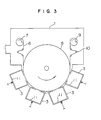
- Fig. 3 illustrates another embodiment, in which a plurality of treatment chambers are disposed against a rotating drum in order to increase the treatment speed.
- this type of devices it is possible to form a multi-layered film by varying treatment conditions and/or the kind of reactive gas for every treatment chamber or to effect other treatments such as plasma cleaning, etching, sputtering, evaporation, etc. at the same time as the formation of the carbon film by varying the structure of specified treatment chambers.
- the high voltage is applied to the rotating electrode 8
- the device cannot have the multiple functions as described above. Consequently these multi-functional characteristics are an auxiliary effect of this invention owing to the fact that the rotating electrode 8 is grounded.
Landscapes
- Physics & Mathematics (AREA)
- Engineering & Computer Science (AREA)
- Plasma & Fusion (AREA)
- Treatments Of Macromolecular Shaped Articles (AREA)
- Physical Vapour Deposition (AREA)
- Chemical Vapour Deposition (AREA)
- ing And Chemical Polishing (AREA)
Applications Claiming Priority (2)
| Application Number | Priority Date | Filing Date | Title |
|---|---|---|---|
| JP61114562A JPS62274080A (ja) | 1986-05-21 | 1986-05-21 | プラズマ処理方法 |
| JP114562/86 | 1986-05-21 |
Publications (3)
| Publication Number | Publication Date |
|---|---|
| EP0248274A2 true EP0248274A2 (fr) | 1987-12-09 |
| EP0248274A3 EP0248274A3 (en) | 1989-11-29 |
| EP0248274B1 EP0248274B1 (fr) | 1993-08-04 |
Family
ID=14640917
Family Applications (1)
| Application Number | Title | Priority Date | Filing Date |
|---|---|---|---|
| EP87107321A Expired - Lifetime EP0248274B1 (fr) | 1986-05-21 | 1987-05-20 | Appareil et méthode de traitement de surface par plasma |
Country Status (5)
| Country | Link |
|---|---|
| US (1) | US5300189A (fr) |
| EP (1) | EP0248274B1 (fr) |
| JP (1) | JPS62274080A (fr) |
| KR (1) | KR910000290B1 (fr) |
| DE (1) | DE3786840T2 (fr) |
Cited By (7)
| Publication number | Priority date | Publication date | Assignee | Title |
|---|---|---|---|---|
| US5224441A (en) * | 1991-09-27 | 1993-07-06 | The Boc Group, Inc. | Apparatus for rapid plasma treatments and method |
| DE4308632A1 (de) * | 1993-03-18 | 1994-09-22 | Leybold Ag | Verfahren und Vorrichtung zum Nachbehandeln von Aluminium-beschichteten Kunststoff-Folien |
| DE4308631A1 (de) * | 1993-03-18 | 1994-09-22 | Leybold Ag | Verfahren und Vorrichtung zur Behandlung unbeschichteter Kunststoff-Folien |
| EP0820852A1 (fr) * | 1996-07-23 | 1998-01-28 | L'air Liquide, Societe Anonyme Pour L'etude Et L'exploitation Des Procedes Georges Claude | Procédé et dispositif de commande du fonctionnement d'un système de traitement de surface d'un substrat solide en défilement |
| EP0820851A1 (fr) * | 1996-07-23 | 1998-01-28 | L'air Liquide, Societe Anonyme Pour L'etude Et L'exploitation Des Procedes Georges Claude | Procédé et dispositif de commande du fonctionnement d'un système de traitement de surface |
| EP2123793A1 (fr) * | 2008-05-20 | 2009-11-25 | Helianthos B.V. | Procédé de dépôt de vapeur |
| EP2899293A4 (fr) * | 2012-09-18 | 2016-06-01 | Lintec Corp | Dispositif d'implantation d'ions |
Families Citing this family (38)
| Publication number | Priority date | Publication date | Assignee | Title |
|---|---|---|---|---|
| IL107827A0 (en) * | 1992-12-08 | 1994-04-12 | Hughes Aircraft Co | Plasma pressure control assembly |
| US6835523B1 (en) * | 1993-05-09 | 2004-12-28 | Semiconductor Energy Laboratory Co., Ltd. | Apparatus for fabricating coating and method of fabricating the coating |
| JP3175894B2 (ja) * | 1994-03-25 | 2001-06-11 | 株式会社半導体エネルギー研究所 | プラズマ処理装置及びプラズマ処理方法 |
| US5534232A (en) * | 1994-08-11 | 1996-07-09 | Wisconsin Alumini Research Foundation | Apparatus for reactions in dense-medium plasmas |
| KR100296692B1 (ko) | 1996-09-10 | 2001-10-24 | 사토 도리 | 플라즈마cvd장치 |
| JP4344019B2 (ja) * | 1997-05-28 | 2009-10-14 | キヤノンアネルバ株式会社 | イオン化スパッタ方法 |
| US6106659A (en) * | 1997-07-14 | 2000-08-22 | The University Of Tennessee Research Corporation | Treater systems and methods for generating moderate-to-high-pressure plasma discharges for treating materials and related treated materials |
| WO1999004411A1 (fr) * | 1997-07-14 | 1999-01-28 | The University Of Tennessee Research Corporation | Systemes de traitement par plasma et procedes de traitement par plasma |
| PT908535E (pt) * | 1997-10-08 | 2003-11-28 | Cockerill Rech & Dev | Processo para a decapagem da superficie de um substrato e instalacao para a colocacao em pratica do referido processo |
| US6082292A (en) * | 1999-01-05 | 2000-07-04 | Wisconsin Alumni Research Foundation | Sealing roller system for surface treatment gas reactors |
| JP2003342739A (ja) * | 2002-05-23 | 2003-12-03 | Sony Corp | プラズマ化学的気相成長装置 |
| KR20040046571A (ko) * | 2002-11-27 | 2004-06-05 | 주식회사 피앤아이 | 이온빔을 이용한 재료의 표면 처리 장치 |
| US20050172897A1 (en) * | 2004-02-09 | 2005-08-11 | Frank Jansen | Barrier layer process and arrangement |
| US7087145B1 (en) | 2005-03-10 | 2006-08-08 | Robert Choquette | Sputtering cathode assembly |
| JP4558810B2 (ja) * | 2008-02-29 | 2010-10-06 | 富士フイルム株式会社 | 成膜装置 |
| JP4999737B2 (ja) * | 2008-03-14 | 2012-08-15 | 富士フイルム株式会社 | 成膜装置 |
| JP5009845B2 (ja) * | 2008-03-14 | 2012-08-22 | 富士フイルム株式会社 | 成膜装置 |
| US20100037824A1 (en) * | 2008-08-13 | 2010-02-18 | Synos Technology, Inc. | Plasma Reactor Having Injector |
| US20100037820A1 (en) * | 2008-08-13 | 2010-02-18 | Synos Technology, Inc. | Vapor Deposition Reactor |
| US8770142B2 (en) * | 2008-09-17 | 2014-07-08 | Veeco Ald Inc. | Electrode for generating plasma and plasma generator |
| US8851012B2 (en) * | 2008-09-17 | 2014-10-07 | Veeco Ald Inc. | Vapor deposition reactor using plasma and method for forming thin film using the same |
| US20100101727A1 (en) * | 2008-10-27 | 2010-04-29 | Helin Ji | Capacitively coupled remote plasma source with large operating pressure range |
| RU2482219C2 (ru) * | 2008-11-05 | 2013-05-20 | Улвак, Инк. | Намоточное вакуумированное устройство |
| EP2379442A4 (fr) * | 2008-12-30 | 2014-02-26 | 3M Innovative Properties Co | Procédé pour la fabrication de surfaces nanostructurées |
| WO2010123528A2 (fr) | 2008-12-30 | 2010-10-28 | 3M Innovative Properties Company | Articles nanostructurés et procédés de fabrication d'articles nanostructurés |
| US8871628B2 (en) * | 2009-01-21 | 2014-10-28 | Veeco Ald Inc. | Electrode structure, device comprising the same and method for forming electrode structure |
| US8257799B2 (en) | 2009-02-23 | 2012-09-04 | Synos Technology, Inc. | Method for forming thin film using radicals generated by plasma |
| US8758512B2 (en) * | 2009-06-08 | 2014-06-24 | Veeco Ald Inc. | Vapor deposition reactor and method for forming thin film |
| EP2360293A1 (fr) * | 2010-02-11 | 2011-08-24 | Nederlandse Organisatie voor toegepast -natuurwetenschappelijk onderzoek TNO | Procédé et appareil pour déposer des couches atomiques sur un substrat |
| US8771791B2 (en) | 2010-10-18 | 2014-07-08 | Veeco Ald Inc. | Deposition of layer using depositing apparatus with reciprocating susceptor |
| US8877300B2 (en) | 2011-02-16 | 2014-11-04 | Veeco Ald Inc. | Atomic layer deposition using radicals of gas mixture |
| US9163310B2 (en) | 2011-02-18 | 2015-10-20 | Veeco Ald Inc. | Enhanced deposition of layer on substrate using radicals |
| US9123507B2 (en) * | 2012-03-20 | 2015-09-01 | Mapper Lithography Ip B.V. | Arrangement and method for transporting radicals |
| US8822314B2 (en) * | 2012-06-14 | 2014-09-02 | Palo Alto Research Center Incorporated | Method of growing epitaxial layers on a substrate |
| JP6045266B2 (ja) * | 2012-09-18 | 2016-12-14 | リンテック株式会社 | イオン注入装置 |
| JP6303733B2 (ja) * | 2014-03-31 | 2018-04-04 | ソニー株式会社 | 磁気記録媒体およびその製造方法、ならびに成膜装置 |
| DE102015222556B3 (de) * | 2015-11-16 | 2017-05-04 | FAP Forschungs- und Applikationslabor Plasmatechnik GmbH Dresden | Vorrichtung zur Modifizierung von Oberflächen von Folien |
| KR20220083082A (ko) * | 2020-12-11 | 2022-06-20 | 한국핵융합에너지연구원 | 통기성 부재의 내면을 플라즈마 처리하는 방법 및 이의 장치 |
Family Cites Families (7)
| Publication number | Priority date | Publication date | Assignee | Title |
|---|---|---|---|---|
| US4013539A (en) * | 1973-01-12 | 1977-03-22 | Coulter Information Systems, Inc. | Thin film deposition apparatus |
| US4322276A (en) * | 1979-06-20 | 1982-03-30 | Deposition Technology, Inc. | Method for producing an inhomogeneous film for selective reflection/transmission of solar radiation |
| JPS5718737A (en) * | 1980-06-21 | 1982-01-30 | Shin Etsu Chem Co Ltd | Apparatus for continuous plasma treatment |
| JPS5754269A (en) * | 1980-09-17 | 1982-03-31 | Matsushita Electric Ind Co Ltd | Apparatus for forming film in vacuum |
| JPS5991130A (ja) * | 1982-11-16 | 1984-05-25 | Matsushita Electric Ind Co Ltd | 高分子基板の表面処理方法 |
| JPS59213735A (ja) * | 1983-05-18 | 1984-12-03 | Kuraray Co Ltd | プラズマ処理方法 |
| US4631105A (en) * | 1985-04-22 | 1986-12-23 | Branson International Plasma Corporation | Plasma etching apparatus |
-
1986
- 1986-05-21 JP JP61114562A patent/JPS62274080A/ja active Pending
-
1987
- 1987-05-14 KR KR1019870004747A patent/KR910000290B1/ko not_active Expired
- 1987-05-20 DE DE87107321T patent/DE3786840T2/de not_active Expired - Fee Related
- 1987-05-20 EP EP87107321A patent/EP0248274B1/fr not_active Expired - Lifetime
- 1987-05-20 US US07/051,701 patent/US5300189A/en not_active Expired - Fee Related
Cited By (14)
| Publication number | Priority date | Publication date | Assignee | Title |
|---|---|---|---|---|
| US5224441A (en) * | 1991-09-27 | 1993-07-06 | The Boc Group, Inc. | Apparatus for rapid plasma treatments and method |
| US5364665A (en) * | 1991-09-27 | 1994-11-15 | The Boc Group, Inc. | Method for rapid plasma treatments |
| DE4308632A1 (de) * | 1993-03-18 | 1994-09-22 | Leybold Ag | Verfahren und Vorrichtung zum Nachbehandeln von Aluminium-beschichteten Kunststoff-Folien |
| DE4308631A1 (de) * | 1993-03-18 | 1994-09-22 | Leybold Ag | Verfahren und Vorrichtung zur Behandlung unbeschichteter Kunststoff-Folien |
| DE4308632B4 (de) * | 1993-03-18 | 2007-10-04 | Applied Materials Gmbh & Co. Kg | Verfahren und Vorrichtung zum Nachbehandeln von Aluminium-beschichteten Kunststoff-Folien |
| FR2751664A1 (fr) * | 1996-07-23 | 1998-01-30 | Air Liquide | Procede et dispositif de commande du fonctionnement d'un systeme de traitement de surface d'un substrat solide en defilement |
| EP0820851A1 (fr) * | 1996-07-23 | 1998-01-28 | L'air Liquide, Societe Anonyme Pour L'etude Et L'exploitation Des Procedes Georges Claude | Procédé et dispositif de commande du fonctionnement d'un système de traitement de surface |
| FR2751665A1 (fr) * | 1996-07-23 | 1998-01-30 | Air Liquide | Procede et dispositif de commande du fonctionnement d'un systeme de traitement de surface |
| US6094606A (en) * | 1996-07-23 | 2000-07-25 | L'air Liquide Societe Anonyme Pour L'etude Et L'exploitation Des Procedes Georges Claude | Control process and device for treating the surface of a solid substrate |
| US6144898A (en) * | 1996-07-23 | 2000-11-07 | L'air Liquide Societe Anonyme Pour L'etude Et L'exploitation Des Procedes Georges Claude | Control process and device for treating the surface of a solid substrate |
| EP0820852A1 (fr) * | 1996-07-23 | 1998-01-28 | L'air Liquide, Societe Anonyme Pour L'etude Et L'exploitation Des Procedes Georges Claude | Procédé et dispositif de commande du fonctionnement d'un système de traitement de surface d'un substrat solide en défilement |
| EP2123793A1 (fr) * | 2008-05-20 | 2009-11-25 | Helianthos B.V. | Procédé de dépôt de vapeur |
| WO2009141304A1 (fr) * | 2008-05-20 | 2009-11-26 | Helianthos B.V. | Processus et dispositif de dépôt en phase vapeur |
| EP2899293A4 (fr) * | 2012-09-18 | 2016-06-01 | Lintec Corp | Dispositif d'implantation d'ions |
Also Published As
| Publication number | Publication date |
|---|---|
| KR870010942A (ko) | 1987-12-19 |
| JPS62274080A (ja) | 1987-11-28 |
| DE3786840D1 (de) | 1993-09-09 |
| EP0248274B1 (fr) | 1993-08-04 |
| DE3786840T2 (de) | 1994-01-20 |
| KR910000290B1 (ko) | 1991-01-24 |
| EP0248274A3 (en) | 1989-11-29 |
| US5300189A (en) | 1994-04-05 |
Similar Documents
| Publication | Publication Date | Title |
|---|---|---|
| EP0248274B1 (fr) | Appareil et méthode de traitement de surface par plasma | |
| KR100502124B1 (ko) | 이동 모재 상에 농후 탄소 코팅을 증착시키기 위한 공정 및 장치 | |
| JP3107971B2 (ja) | 気相反応装置 | |
| US5888594A (en) | Process for depositing a carbon-rich coating on a moving substrate | |
| US6183816B1 (en) | Method of fabricating the coating | |
| US6001431A (en) | Process for fabricating a magnetic recording medium | |
| JPS6283471A (ja) | 炭素皮膜形成方法及び装置 | |
| EP0561243B1 (fr) | Dispositif pour CVD assisté par plasma et procédé correspondant | |
| EP0046090B1 (fr) | Procédé de fabrication d'un matériau d'enregistrement magnétique | |
| JPH0610871B2 (ja) | 磁気記録媒体 | |
| CA1162113A (fr) | Methode de production de supports d'enregistrement magnetique | |
| US7264850B1 (en) | Process for treating a substrate with a plasma | |
| JPH0352937A (ja) | 連続式プラズマ処理装置 | |
| JPH07166356A (ja) | 基板の表面処理方法 | |
| JPH1087397A (ja) | 硬質炭素被膜、及び該被膜を用いた電気シェーバー刃 | |
| US6223686B1 (en) | Apparatus for forming a thin film by plasma chemical vapor deposition | |
| JP3014289B2 (ja) | 硬質カーボン膜の形成方法 | |
| JP3145243B2 (ja) | 被膜形成装置 | |
| US6060131A (en) | Method of forming a thin film by plasma chemical vapor deposition | |
| JPH0674505B2 (ja) | 炭素皮膜形成方法および装置 | |
| JP3831424B2 (ja) | 磁気記録媒体の製造方法 | |
| JPH10298758A (ja) | 薄膜製造方法及び装置 | |
| JP2002030446A (ja) | 成膜方法、成膜装置、磁気テープの製造方法及びその装置 | |
| JPH10237663A (ja) | プラズマ重合膜の形成方法およびプラズマ重合膜形成装置 | |
| JP2878468B2 (ja) | 長尺薄板用プラズマ発生方法及び装置 |
Legal Events
| Date | Code | Title | Description |
|---|---|---|---|
| PUAI | Public reference made under article 153(3) epc to a published international application that has entered the european phase |
Free format text: ORIGINAL CODE: 0009012 |
|
| AK | Designated contracting states |
Kind code of ref document: A2 Designated state(s): DE FR GB |
|
| PUAL | Search report despatched |
Free format text: ORIGINAL CODE: 0009013 |
|
| AK | Designated contracting states |
Kind code of ref document: A3 Designated state(s): DE FR GB |
|
| 17P | Request for examination filed |
Effective date: 19891109 |
|
| 17Q | First examination report despatched |
Effective date: 19910627 |
|
| GRAA | (expected) grant |
Free format text: ORIGINAL CODE: 0009210 |
|
| AK | Designated contracting states |
Kind code of ref document: B1 Designated state(s): DE FR GB |
|
| REF | Corresponds to: |
Ref document number: 3786840 Country of ref document: DE Date of ref document: 19930909 |
|
| ET | Fr: translation filed | ||
| PLBE | No opposition filed within time limit |
Free format text: ORIGINAL CODE: 0009261 |
|
| STAA | Information on the status of an ep patent application or granted ep patent |
Free format text: STATUS: NO OPPOSITION FILED WITHIN TIME LIMIT |
|
| 26N | No opposition filed | ||
| REG | Reference to a national code |
Ref country code: GB Ref legal event code: IF02 |
|
| PGFP | Annual fee paid to national office [announced via postgrant information from national office to epo] |
Ref country code: GB Payment date: 20040428 Year of fee payment: 18 Ref country code: FR Payment date: 20040428 Year of fee payment: 18 |
|
| PGFP | Annual fee paid to national office [announced via postgrant information from national office to epo] |
Ref country code: DE Payment date: 20040608 Year of fee payment: 18 |
|
| PG25 | Lapsed in a contracting state [announced via postgrant information from national office to epo] |
Ref country code: GB Free format text: LAPSE BECAUSE OF NON-PAYMENT OF DUE FEES Effective date: 20050520 |
|
| PG25 | Lapsed in a contracting state [announced via postgrant information from national office to epo] |
Ref country code: DE Free format text: LAPSE BECAUSE OF NON-PAYMENT OF DUE FEES Effective date: 20051201 |
|
| GBPC | Gb: european patent ceased through non-payment of renewal fee |
Effective date: 20050520 |
|
| PG25 | Lapsed in a contracting state [announced via postgrant information from national office to epo] |
Ref country code: FR Free format text: LAPSE BECAUSE OF NON-PAYMENT OF DUE FEES Effective date: 20060131 |
|
| REG | Reference to a national code |
Ref country code: FR Ref legal event code: ST Effective date: 20060131 |