EP0248353A2 - Circuit d'adresse de mémoire permettant d'échanger des bits sélectionnés d'une entrée d'adresse - Google Patents
Circuit d'adresse de mémoire permettant d'échanger des bits sélectionnés d'une entrée d'adresse Download PDFInfo
- Publication number
- EP0248353A2 EP0248353A2 EP87107767A EP87107767A EP0248353A2 EP 0248353 A2 EP0248353 A2 EP 0248353A2 EP 87107767 A EP87107767 A EP 87107767A EP 87107767 A EP87107767 A EP 87107767A EP 0248353 A2 EP0248353 A2 EP 0248353A2
- Authority
- EP
- European Patent Office
- Prior art keywords
- decoder
- address
- memory
- bit
- bits
- Prior art date
- Legal status (The legal status is an assumption and is not a legal conclusion. Google has not performed a legal analysis and makes no representation as to the accuracy of the status listed.)
- Granted
Links
- 239000000872 buffer Substances 0.000 description 7
- 108091047102 miR-4 stem-loop Proteins 0.000 description 6
- 108091049748 miR-4-1 stem-loop Proteins 0.000 description 6
- 108091058497 miR-4-2 stem-loop Proteins 0.000 description 6
- 108091048196 miR-5 stem-loop Proteins 0.000 description 6
- 108091082444 miR-5-1 stem-loop Proteins 0.000 description 6
- 108091078363 miR-5-2 stem-loop Proteins 0.000 description 6
- 108091028606 miR-1 stem-loop Proteins 0.000 description 5
- 238000010586 diagram Methods 0.000 description 4
- 230000003247 decreasing effect Effects 0.000 description 2
- 239000011159 matrix material Substances 0.000 description 2
- 230000000694 effects Effects 0.000 description 1
- 238000013507 mapping Methods 0.000 description 1
- 108091063445 miR-13 stem-loop Proteins 0.000 description 1
- 238000012986 modification Methods 0.000 description 1
- 230000004048 modification Effects 0.000 description 1
Images

Classifications
-
- G—PHYSICS
- G11—INFORMATION STORAGE
- G11C—STATIC STORES
- G11C8/00—Arrangements for selecting an address in a digital store
Definitions
- the present invention relates to a memory incorporated in a microcomputer, and more particularly to an address circuit associated with a read only memory.
- a microcomputer such as a one-chip microcomputer comprises a read only memory (ROM) storing a microprogram for controlling an operation of the microcomputer.
- ROM read only memory
- a ROM 10 is associated with an address circuit which is composed of an X-decoder 12 and a Y-decoder 14. These decoders 12 and 14 are adapted to receive respective allocated portions of a given address signal through buses 16 and 18, respectively.
- the X-decoder 12 and the Y-decoder 14 cooperate to allow a data or microinstruction designated by the given address signal to be read out through an output 20.
- the capacity or size of the ROM is determined, the sum of the input numbers of the X-decoder 12 and the Y-decoder 14 is directly decided. Namely, if the number of inputs of the X-decoder is settled, the input number of the Y-decoder is accordingly determined. In addition, the numbers of the respective outputs of the X- and Y- decoders are also decided. These output numbers of the decoders and the output bit number of the ROM will determine the size of the ROM 10 in the X direction and in the Y direction.
- the conventional address circuits of the ROM have been adapted to distribute all bits of an input address signal to the X-decoder and the Y-decoder, so that the input address signal is full-decoded without exception. Therefore, even if the ROM includes addresses which are never accessed, the X-decoder and the Y-decoder had to comprise all circuits required for full-decoding the input address. This will result in wasteful increase of a LSI chip size.
- Another object of the present invention to provide an address circuit which is associated to a read only memory and which makes it possible to save the chip size.
- Still another object of the present invention is to provide a memory address circuit which includes an X-decoder and Y-decoder and which can save circuit elements of the X- or Y- decoder when a memory has an address that is never accessed.
- a memory associated with an address circuit receiving an address signal to designate a location of the memory to be accessed, the address circuit including an X-decoder and a Y-decoder associated to the memory, and a multiplexor receiving at least a portion of an address input and adapted to selectively distribute the above portion of the address input to the X-decoder and the Y-decoder.
- the multiplexor receives at least one first bit of a portion of the address signal to be inputted to the X-decoder and at least one second bit of the remaining portion of the address signal to be inputted to the Y-decoder. In a first condition, the multiplexor operates to supply the first bit and the second bit of the address input to the X-decoder and the Y-decoder, respectively. In a second condition, the multiplexor operates to supply the first bit and the second bit of the address input to the Y-decoder and the X-decoder, respectively.
- the multiplexor can mutually exchange a portion of the address to the X-decoder and a portion of the address to the X-decoder. Therefore, the exchange of these address portions is so set that empty addresses being never accessed are collected to one or more output or decode lines of the X- or Y-decoder.
- a circuit associated to the output line of the decoder can be omitted.
- the number of circuit elements required for the X- or Y-decoder can be decreased, which will result in decrease of a chip area necessary for the memory and in increase of an operation speed of the memory.
- a read only memory (ROM) 30 of the matrix structure is associated with an X-decoder 32 and a Y-decoder 34 which are adapted to receive respectively allocated bits of an address input.
- the X-decoder 32 operates to enable one of lines 36 connected to the ROM 30, and the Y-decoder 34 operates to enable one set of a plurality of sets of lines 38 connected to the ROM 30, so that a data or microinstruction designated by the address input is read out through an output 40.
- a multiplexor 42 adapted to receive a portion of the address input and having a pair of outputs 44 and 46 connected to the X-decoder 32 and the Y-decoder 34, respectively.
- the address input is divided into four portions 48, 50, 52 and 54. The first portion of the address input is directly inputted to the X-decoder 32. The second and third portions 50 and 52 are inputted to the multiplexor 42.
- the multiplexor 42 is controlled by a selection signal MIRXG to supply the second and third portions 50 and 52 to the X-decoder 32 and the Y-decoder 34, respectively, when it is in a first condition, and also to supply the second and third portions 50 and 52 to the Y-decoder 34 and the X-decoder 32, respectively, when it is in a second condition.
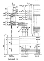
- a ROM 60 is of a matrix structure having a plurality of word lines 62 and a plurality of bit lines 64 orthogonal to the word lines 62. At each of intersections between the word lines 62 and the bit lines 64, there is located one MOS transistor 66 constituting one elementary memory. As seen from the drawing, the shown ROM 60 is of a word structure having each word consisting of 12 bits.
- Each four lines of the bit lines 64 are connected through transfer gates 68 provided in a Y-decoder 70 commonly to an input of one corresponding tristate output buffer 72 provided in an output circuit 74.
- These output buffers 72 are controlled by a ROM read signal MROMRD, and connected at their output terminal to corresponding lines of a bus 76.
- Each of the word lines 62 is selectively enabled by an associated X-decoder 78, which can be a well-known one.
- An address signal to be inputted to the ROM shown in Figure 3 is composed of 14 bits of MIR 0 to MIR 13. Two least significant bits MIR 0 and MIR 1 of the address signal are ordinarily supplied through a multiplexor 80 to a decoding section 82 of the Y-decoder 70.
- the decoding section 82 of the Y-decoder 70 includes a pair of inverters 84 and four AND gates 86 connected as shown to decode a two-bit input so as to enable one selected transfer gate 68 of each set consisting of four transfer gates.
- the multiplexor 80 includes four first transfer gates 88 connected between the address inputs MIR 0, MIR 1, MIR 4 and MIR 5 and the decoding section 82 of the Y-decoder 70 and the input of the X-decoder 78, respectively.
- the multiplexor 80 also includes four second transfer gates 90 connected between the address inputs MIR 0, MIR 1, MIR 4 and MIR 5 and the input of the X-decoder 78 and the decoding section 82 of the Y-decoder 70.
- the first transfer gates 88 are connected at their control terminals to an output of an inverter 92, and the second transfer gates 90 have their control terminals connected to an input of the inverter 92, which is connected to an output of another inverter 94 adapted to receive at its input the selection signal MIRXG.
- the transfer gates 88 are on and the transfer gates 90 are off, so that the address input MIR 0, MIR 1, MIR 4 and MIR 5 are supplied to the decoding section 82 of the Y-decoder 70 and the input of the X-decoder 78, respectively.
- the transfer gates 88 are off and the transfer gates 90 are on, so that the address inputs MIR 0 and MIR 1 are supplied to the X-decoder 78 and the address inputs MIR 4 and the MIR 5 are supplied to the decoding section 82 of the Y-decoder 70.
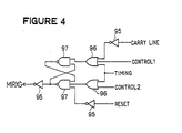
- FIG 4 there is shown one example of a circuit for generating the selection signal MIRXG.
- the shown circuit includes three inverters 95, two OR gates 96 and two AND gates 97 connected as shown to receive a carry line of a ROM address generator (not shown), control signals 1 and 2, a timing signal and a reset signal.
- the ROM 30 has a plurality of empty addresses which are never accessed. Therefore, by generating the selection signal MIRXG from the address signal so as to mutually exchange one or more input bits of the X-decoder and the corresponding number of input bits of the Y-decoder, one output of the X- or Y-decoder can be assigned to the empty area of address. Therefore, the number of the output lines of the X- or Y-decoder can be decreased.
- the above TABLE shows one example of an address mapping.
- the address space includes four empty addresses A, E, F and G and three use addresses B, C and D. Therefore, if the two least significant two bits "1" and "LSB" are mutually exchanged by the two bits "4" and "5", the addresses B, C and D are replaced by the addresses E, F and G, respectively. With this exchange of the address bits and the empty address A, a decode line for "100010" of the Y-decoder can be omitted.
- a decode line for the X-decode can be also omitted in a similar manner.
- each output buffer of the X-decoder includes two NAND gates and one inverter.
- 214 x 12 transistors are required as memory elements.
- 12 output buffers 72 transistors
- 12 sense amplifiers are required.
- 4 buffers (8 transistors) are required for the Y-decoder. Totally, 196700 transistors are required.
- the memory itself contains 20544 transistors. But, 428 output buffers (2568 transistors) are required for the X-decoder. The 12 sense amplifiers and the four buffers for the Y-decoder are still required. Further, a MIRXG signal generator requires about 40 transistors. Therefore, the total number is 23172. Namely, the required number of element is reduced to about 12 %. In addition, the required layout area is reduced to about 45 %.
- the word number and the bit length of the memory structure can be changed without modifying the bit length of the address signal.
- the capacity of the memory can be easily reduced without changing the format of the address signal.
Landscapes
- Engineering & Computer Science (AREA)
- Microelectronics & Electronic Packaging (AREA)
- Read Only Memory (AREA)
- Static Random-Access Memory (AREA)
- Microcomputers (AREA)
Applications Claiming Priority (2)
| Application Number | Priority Date | Filing Date | Title |
|---|---|---|---|
| JP12265986A JPH0795398B2 (ja) | 1986-05-27 | 1986-05-27 | 1チップマイクロコンピュータ |
| JP122659/86 | 1986-05-27 |
Publications (3)
| Publication Number | Publication Date |
|---|---|
| EP0248353A2 true EP0248353A2 (fr) | 1987-12-09 |
| EP0248353A3 EP0248353A3 (en) | 1990-05-23 |
| EP0248353B1 EP0248353B1 (fr) | 1993-11-03 |
Family
ID=14841453
Family Applications (1)
| Application Number | Title | Priority Date | Filing Date |
|---|---|---|---|
| EP87107767A Expired - Lifetime EP0248353B1 (fr) | 1986-05-27 | 1987-05-27 | Circuit d'adresse de mémoire permettant d'échanger des bits sélectionnés d'une entrée d'adresse |
Country Status (4)
| Country | Link |
|---|---|
| US (1) | US4831587A (fr) |
| EP (1) | EP0248353B1 (fr) |
| JP (1) | JPH0795398B2 (fr) |
| DE (1) | DE3788000T2 (fr) |
Families Citing this family (2)
| Publication number | Priority date | Publication date | Assignee | Title |
|---|---|---|---|---|
| US5640338A (en) * | 1995-12-07 | 1997-06-17 | Hyundai Electronics Industries Co. Ltd. | Semiconductor memory device |
| US6567289B1 (en) | 2000-08-23 | 2003-05-20 | Advanced Micro Devices, Inc. | Physical memory layout with various sized memory sectors |
Family Cites Families (3)
| Publication number | Priority date | Publication date | Assignee | Title |
|---|---|---|---|---|
| US4117470A (en) * | 1976-10-08 | 1978-09-26 | Data General Corporation | Data bit compression system |
| US4651275A (en) * | 1981-07-02 | 1987-03-17 | Texas Instruments Incorporated | Microcomputer having read/write memory for combined macrocode and microcode storage |
| FR2540277A1 (fr) * | 1983-02-01 | 1984-08-03 | Brion Alain | Memoire de mots munie d'un circuit de transcodage d'adresses |
-
1986
- 1986-05-27 JP JP12265986A patent/JPH0795398B2/ja not_active Expired - Fee Related
-
1987
- 1987-05-27 DE DE87107767T patent/DE3788000T2/de not_active Expired - Fee Related
- 1987-05-27 US US07/071,519 patent/US4831587A/en not_active Expired - Lifetime
- 1987-05-27 EP EP87107767A patent/EP0248353B1/fr not_active Expired - Lifetime
Also Published As
| Publication number | Publication date |
|---|---|
| JPS62279594A (ja) | 1987-12-04 |
| DE3788000D1 (de) | 1993-12-09 |
| JPH0795398B2 (ja) | 1995-10-11 |
| EP0248353B1 (fr) | 1993-11-03 |
| EP0248353A3 (en) | 1990-05-23 |
| US4831587A (en) | 1989-05-16 |
| DE3788000T2 (de) | 1994-02-24 |
Similar Documents
| Publication | Publication Date | Title |
|---|---|---|
| US4566082A (en) | Memory pack addressing system | |
| US4694394A (en) | Microprocessor system having a multiplexed address/data bus which communicates with a plurality of memory and input/output devices including TTL output gates | |
| US5148396A (en) | Semiconductor integrated circuit memory enabling memory write masking | |
| US5025415A (en) | Memory card | |
| EP0299697A2 (fr) | Dispositif de circuit intégré à semi-conducteurs | |
| KR910000388B1 (ko) | 메모리셀 블록의 선택적 동작이 가능한 반도체 메모리장치 | |
| EP0443775A2 (fr) | Circuit de signature pour un dispositif de mémoire non-volatile | |
| US5243701A (en) | Method of and system for processing data having bit length variable with modes of operation | |
| US5446859A (en) | Register addressing control circuit including a decoder and an index register | |
| US5179676A (en) | Address selection circuit including address counters for performing address selection | |
| US5426432A (en) | IC card | |
| EP0248353B1 (fr) | Circuit d'adresse de mémoire permettant d'échanger des bits sélectionnés d'une entrée d'adresse | |
| JP2003223412A (ja) | 半導体集積回路 | |
| US5101376A (en) | Integrated microprocessor with associative memory device | |
| US5504710A (en) | Semiconductor memory device having a bit control circuit | |
| US6499089B1 (en) | Method, architecture and circuitry for independently configuring a multiple array memory device | |
| US4809229A (en) | Data processing integrated circuit with improved decoder arrangement | |
| EP0234187A2 (fr) | Mécanisme de transfert contrôlé par programme dans une unité programmable avec des largeurs de voie de données variables | |
| EP0517260A1 (fr) | Circuit de mémoire semi-conducteur avec focntion pour effacement de bit et/ou fonction pour initialisation de registre | |
| EP0157341B1 (fr) | Circuit d'interface de mémoire | |
| JP3965620B2 (ja) | 記憶装置および記憶方法並びにデータ処理システム | |
| US4152778A (en) | Digital computer memory | |
| KR0166650B1 (ko) | 멀티플렉스용 입출력 포트를 가진 마이크로 프로세서 | |
| JPH0218728B2 (fr) | ||
| KR850000710B1 (ko) | 일정번지수 영역을 공통으로 사용하는 다수 메모리뱅크 시스템 |
Legal Events
| Date | Code | Title | Description |
|---|---|---|---|
| PUAI | Public reference made under article 153(3) epc to a published international application that has entered the european phase |
Free format text: ORIGINAL CODE: 0009012 |
|
| 17P | Request for examination filed |
Effective date: 19870527 |
|
| AK | Designated contracting states |
Kind code of ref document: A2 Designated state(s): DE GB IT |
|
| PUAL | Search report despatched |
Free format text: ORIGINAL CODE: 0009013 |
|
| AK | Designated contracting states |
Kind code of ref document: A3 Designated state(s): DE GB IT |
|
| 17Q | First examination report despatched |
Effective date: 19910723 |
|
| GRAA | (expected) grant |
Free format text: ORIGINAL CODE: 0009210 |
|
| AK | Designated contracting states |
Kind code of ref document: B1 Designated state(s): DE GB IT |
|
| PG25 | Lapsed in a contracting state [announced via postgrant information from national office to epo] |
Ref country code: IT Free format text: LAPSE BECAUSE OF FAILURE TO SUBMIT A TRANSLATION OF THE DESCRIPTION OR TO PAY THE FEE WITHIN THE PRE;WARNING: LAPSES OF ITALIAN PATENTS WITH EFFECTIVE DATE BEFORE 2007 MAY HAVE OCCURRED AT ANY TIME BEFORE 2007. THE CORRECT EFFECTIVE DATE MAY BE DIFFERENT FROM THE ONE RECORDED.SCRIBED TIME-LIMIT Effective date: 19931103 |
|
| REF | Corresponds to: |
Ref document number: 3788000 Country of ref document: DE Date of ref document: 19931209 |
|
| PLBE | No opposition filed within time limit |
Free format text: ORIGINAL CODE: 0009261 |
|
| STAA | Information on the status of an ep patent application or granted ep patent |
Free format text: STATUS: NO OPPOSITION FILED WITHIN TIME LIMIT |
|
| 26N | No opposition filed | ||
| REG | Reference to a national code |
Ref country code: GB Ref legal event code: IF02 |
|
| REG | Reference to a national code |
Ref country code: GB Ref legal event code: 732E |
|
| PGFP | Annual fee paid to national office [announced via postgrant information from national office to epo] |
Ref country code: GB Payment date: 20040526 Year of fee payment: 18 |
|
| PGFP | Annual fee paid to national office [announced via postgrant information from national office to epo] |
Ref country code: DE Payment date: 20040603 Year of fee payment: 18 |
|
| PG25 | Lapsed in a contracting state [announced via postgrant information from national office to epo] |
Ref country code: GB Free format text: LAPSE BECAUSE OF NON-PAYMENT OF DUE FEES Effective date: 20050527 |
|
| PG25 | Lapsed in a contracting state [announced via postgrant information from national office to epo] |
Ref country code: DE Free format text: LAPSE BECAUSE OF NON-PAYMENT OF DUE FEES Effective date: 20051201 |
|
| GBPC | Gb: european patent ceased through non-payment of renewal fee |
Effective date: 20050527 |