EP0249256B1 - Halbleiteranordnung mit einer Aluminium-Verbindungsschicht mit geringem Vanadium-Prozentgehalt - Google Patents
Halbleiteranordnung mit einer Aluminium-Verbindungsschicht mit geringem Vanadium-Prozentgehalt Download PDFInfo
- Publication number
- EP0249256B1 EP0249256B1 EP87200642A EP87200642A EP0249256B1 EP 0249256 B1 EP0249256 B1 EP 0249256B1 EP 87200642 A EP87200642 A EP 87200642A EP 87200642 A EP87200642 A EP 87200642A EP 0249256 B1 EP0249256 B1 EP 0249256B1
- Authority
- EP
- European Patent Office
- Prior art keywords
- vanadium
- layer
- aluminium
- semiconductor device
- small percentage
- Prior art date
- Legal status (The legal status is an assumption and is not a legal conclusion. Google has not performed a legal analysis and makes no representation as to the accuracy of the status listed.)
- Expired - Lifetime
Links
Images

Classifications
-
- H—ELECTRICITY
- H10—SEMICONDUCTOR DEVICES; ELECTRIC SOLID-STATE DEVICES NOT OTHERWISE PROVIDED FOR
- H10W—GENERIC PACKAGES, INTERCONNECTIONS, CONNECTORS OR OTHER CONSTRUCTIONAL DETAILS OF DEVICES COVERED BY CLASS H10
- H10W20/00—Interconnections in chips, wafers or substrates
- H10W20/40—Interconnections external to wafers or substrates, e.g. back-end-of-line [BEOL] metallisations or vias connecting to gate electrodes
- H10W20/41—Interconnections external to wafers or substrates, e.g. back-end-of-line [BEOL] metallisations or vias connecting to gate electrodes characterised by their conductive parts
- H10W20/44—Conductive materials thereof
- H10W20/4403—Conductive materials thereof based on metals, e.g. alloys, metal silicides
- H10W20/4405—Conductive materials thereof based on metals, e.g. alloys, metal silicides the principal metal being aluminium
- H10W20/4407—Aluminium alloys
Definitions
- This invention relates to a semiconductor device having a body and a patterned electrically conductive layer consisting of aluminium with a small percentage of vanadium on a surface of said body and a method of producing it.
- Aluminium is the principal conductive material employed for electrical interconnection in semiconductor devices.
- the top interconnection layer in an integrated circuit nearly always consists of an aluminium alloy.
- the reasons for the predominance of aluminium includes low resistivity, good adherence to silicon dioxide, low cost, ease in bonding, and good etchability.
- electromigration One of the main phenomena that cause an interconnect layer to degrade is electromigration in which atoms of the interconnect physically change location as current passes through the interconnect.
- the circuit resistance increases.
- An open-circuit failure may occur. If the interconnect layer consists of pure aluminium, failure through electromigration typically occurs much faster than desirable.
- One or more impurities are often used in the aluminium to inhibit electromigration.
- an aluminium alloy formed with 1% silicon by weight and from 0.5% to 4% copper by weight has considerably better electromigration resistance than pure aluminium , see J. Towner, "Electromigration Testing of Thin Films at the Wafer Level," Solid State Technology, Vol. 27, Oct. 1984, pp. 197-200.
- Copper does not form a volatile halide. This limits the usage of copper in situations where it is desirable to etch the interconnect with a halogen-based plasma.
- H. Howard et al specify that electromigration can be reduced by using a multi-phase aluminium alloy in which there are regions containing one or more intermetallic compounds formed with aluminium and at least one transition metal.
- the intermetallic material consists of at least 2% of the interconnect by weight.
- the device and process of Howard et al which corresponds to the preambles of claims 1 and 4, involves depositing aluminium and the transition metal(s) on a body such as a semiconductor device, annealing the structure at a sufficiently high temperature to produce the intermetallic compound(s), and then removing portions of the resulting alloy layer to define the interconnect in a multi-phase crystal-structure.
- vanadium which (according to Howard et al) forms VAl7 and V4Al23 as intermetallic species.
- the work with vanadium is of interest because it forms a volatile halide and is therefore quite suitable to plasma etching.
- resistivity of the Al-V alloy of Howard et al would be too high for numerous future integrated circuit applications.
- the structure with the patterned electrically conductive layer which consists of aluminium with a small percentage of vanadium is characterized in that the layer contains 0,01 - 0,3% vanadium by weight which is in solid solution distributed uniformly throughout the layer.
- the structure is created by depositing a layer of aluminium and vanadium in the necessary proportions on the body after which the layer is patterned and annealed.
- the present vanadium-containing aluminium alloy has excellent electromigration resistance, particularly at the 0.3% vanadium level.
- the worst-case resistivity is only about 30% greater than that of pure aluminium, making the alloy quite acceptable for integrated circuit usage.
- the upper surface of the patterned layer is considerably smoother than that formed with pure aluminium or an aluminium alloy having a small amount of silicon.
- the small percentage of vanadium should not affect substrate adhesion or bondability.
- the present alloy can be readily etched with halogen-based plasmas.
- Fig. 1 illustrates a structure in which a patterned electrically conductive interconnect layer 10 lies on the upper surface of a body 12 consisting of a monocrystalline silicon substrate 14 and an overlying layer 16 of silicon dioxide.
- Substrate 14 may contain various N-type and P-type regions (not shown).
- Interconnect layer 10 contacts certain of these doped regions by way of apertures through insulating layer 16 of which Fig. 1 indicates one such aperture 18.
- a thin layer (not shown) of a barrier metal such as tungsten or titanium-tungsten may lie in aperture 18 between layer 10 and substrate 14.
- Interconnect layer 10 consists of aluminium with 0.01 % - 0.3% vanadium by weight.
- the two metals are substantially in a single-phase crystal structure, sometimes referred to as a solid solution, in which the vanadium is distributed substantially uniformly throughout the aluminium.
- Layer 10 contains essentially no intermetallic compounds formed with vanadium and aluminium.
- the equilibrium solid solubility of vanadium in aluminium is about 0.13 wt % V at 450°C.
- the components of layer 10 unqualifiedly form a single phase if the vanadium concentration is about 0.13 wt % or less. There is no significant change if the amount of vanadium rises to 0.3 wt %.
- no V-Al intermetallic compounds were clearly discernible during transmission electron microscope analysis of a post-annealed (35 minutes at 450°C) sample of conductor 10 containing about 0.2 wt % V. Little intermetallic compound formation was observed in a post-annealed (35 minutes at 450°C) sample having about 0.4 wt % V. From this, it appears that the aluminium and vanadium in layer 10 are essentially in a single crystal phase for the 0.13 - 0.3 wt % V range.
- the single-phase structure in layer 10 may result in a higher resistivity than that which would exist if the crystal structure were multi-phase with one or more intermetallic compounds present. However, the single phase appears to reduce susceptability to corrosion and to facilitate etching with halogen-based plasmas.
- Layer 10 may also contain up to 4 wt % silicon distributed substantially uniformly throughout the aluminium and vanadium. If any silicon is present, the amount is usually 1 wt %. Although silicon does not form a silicide with aluminium, the silicon present in layer 10 makes it easier to form intermetallic compounds. Nonetheless, it appears that layer 10 contains little, if any, Al-V-Si compounds when the amounts of vanadium and silicon are respectively no more than 0.3 wt & and 1 wt %.
- Figs. 2a - 2d illustrate how the structure of Fig. 1 is fabricated.
- the starting material is body 12 in which oxide layer 16 is formed according to conventional thermal oxidation or deposition techniques along the top of substrate 14.
- Aperture 18 is cut through dielectric 16 using conventional masking and etching processes to produce the structure shown in Fig. 2a.
- the barrier metal layer if present, is then formed according to conventional techniques.
- the structure is placed in the deposition chamber of a sputtering apparatus such as a multi-pass DC planar magnetron system.
- the chamber is pump o a low pressure (e.g., 7 ⁇ 10 ⁇ 5 Pa) and back filled with argon to a maximum pressure of 25 Pa.
- the chamber pressure is preferably about 0.2 Pa.
- Aluminium and vanadium are then sputtered from a single deposition source at a target power of 1.6 kilowatts to form a conductive layer 20 consisting of aluminium with a small amount of vanadium at a selected value in the range from 0.01 - 0.3 wt %. If the final alloy is to contain some silicon, it is also provided from the deposition source.
- the thickness of layer 20 is about 0.5 micron.
- the structure appears as indicated in Fig. 2b.
- a photoresist mask 22 is formed on the top layer 20 as indicated in Fig. 2c.
- the exposed portion of layer 20 is removed with a conventional Cl containing plasma to define patterned interconnect layer 10 as depicted in Fig. 2d.
- Mask 22 is removed to produce the structure of Fig. 1.
- the structure is now annealed for 10 to 480 minutes at a temperature in the range from 400 to 500°C.
- the annealing step is preferably done at 450°C for 30 - 35 minutes.
- the anneal stabilizes the grain structure in layer 10, lowers its resistivity, and ensures good contact to substrate 14.
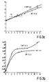
- Fig. 3a shows experimental data for the variance of resistivity as a function of vanadium concentration for samples of conductor 10 having 0 wt % Si and 1 wt % Si.
- the maximum acceptable concentration of vanadium in the alloy i.e., layer 10 or 20 was around 0.3 wt % vanadium.
- Fig. 3b shows test results for Al-V alloys having 0 wt % Si and 1 wt % Si. As indicated there, the median time to failure rises from a relatively low level when no vanadium is present to approximately a plateau near 0.3 wt % vanadium.
Landscapes
- Internal Circuitry In Semiconductor Integrated Circuit Devices (AREA)
Claims (4)
- Halbleiteranordnung mit einem Körper, auf dessen Oberfläche eine mit einem Muster versehene elektrisch leitende Schicht vorgesehen ist, die aus Aluminium mit einem geringen Vanadiumgehalt besteht, dadurch gekennzeichnet, daß die Schicht 0,01 - 0,3 Gew.% Vanadium aufweist, das in fester Lösung einheitlich über die Schicht verteilt ist.
- Anordnung nach Anspruch 1, dadurch gekennzeichnet, daß die Schicht mehr als 0,13 Gew.% Vanadium aufweist.
- Anordnung nach Anspruch 1 oder 2, dadurch gekennzeichnet, daß die Schicht bis zu 4 Gew.% Silizium aufweist.
- Verfahren zum Herstellen einer Halbleiteranordnung nach Anspruch 1, wobei die elektrisch leitende Schicht aus Aluminium mit einem geringen Prozentsatz Vanadium auf einer Oberfläche des genannten Körpers angebracht wird, wonach die Schicht mit einem Muster versehen und geglüht wird, dadurch gekennzeichnet, daß die Schicht durch Zerstäubung von Aluminium und Vanadium aus einer einzigen Quelle derart angebracht wird, daß die angebrachte Schicht 0,01 - 0,3 Gew.% Vanadium aufweist und daß die Schicht während einer Zeit im Bereich von 10 Minuten bis 480 Minuten bei einer Temperatur im Bereich von 400°C bis 500°C geglüht wird.
Applications Claiming Priority (2)
| Application Number | Priority Date | Filing Date | Title |
|---|---|---|---|
| US85164886A | 1986-04-14 | 1986-04-14 | |
| US851648 | 1986-04-14 |
Publications (3)
| Publication Number | Publication Date |
|---|---|
| EP0249256A2 EP0249256A2 (de) | 1987-12-16 |
| EP0249256A3 EP0249256A3 (en) | 1988-05-04 |
| EP0249256B1 true EP0249256B1 (de) | 1992-01-22 |
Family
ID=25311300
Family Applications (1)
| Application Number | Title | Priority Date | Filing Date |
|---|---|---|---|
| EP87200642A Expired - Lifetime EP0249256B1 (de) | 1986-04-14 | 1987-04-06 | Halbleiteranordnung mit einer Aluminium-Verbindungsschicht mit geringem Vanadium-Prozentgehalt |
Country Status (4)
| Country | Link |
|---|---|
| EP (1) | EP0249256B1 (de) |
| JP (1) | JPH07111970B2 (de) |
| KR (1) | KR960000703B1 (de) |
| DE (1) | DE3776203D1 (de) |
Families Citing this family (3)
| Publication number | Priority date | Publication date | Assignee | Title |
|---|---|---|---|---|
| KR100228414B1 (ko) * | 1991-01-17 | 1999-11-01 | 가토 유이치 | 알루미늄 합금 배선층과 그의 제법, 및 알루미늄 합금 스퍼터링 타겟 |
| US5330629A (en) * | 1992-12-15 | 1994-07-19 | At&T Bell Laboratories | Method for depositing aluminum layers on insulating oxide substrates |
| US6965190B2 (en) | 2001-09-12 | 2005-11-15 | Sanyo Electric Co., Ltd. | Surface acoustic wave device |
Citations (1)
| Publication number | Priority date | Publication date | Assignee | Title |
|---|---|---|---|---|
| US4017890A (en) * | 1975-10-24 | 1977-04-12 | International Business Machines Corporation | Intermetallic compound layer in thin films for improved electromigration resistance |
Family Cites Families (5)
| Publication number | Priority date | Publication date | Assignee | Title |
|---|---|---|---|---|
| JPS58103168A (ja) * | 1981-12-16 | 1983-06-20 | Fujitsu Ltd | 半導体装置 |
| US4525734A (en) * | 1983-03-21 | 1985-06-25 | Syracuse University | Hydrogen charged thin film conductor |
| US4566177A (en) * | 1984-05-11 | 1986-01-28 | Signetics Corporation | Formation of electromigration resistant aluminum alloy conductors |
| JPS6193647A (ja) * | 1984-10-12 | 1986-05-12 | Fujitsu Ltd | 半導体装置 |
| JPS6199372A (ja) * | 1984-10-22 | 1986-05-17 | Hitachi Ltd | 電極配線 |
-
1987
- 1987-04-06 EP EP87200642A patent/EP0249256B1/de not_active Expired - Lifetime
- 1987-04-06 DE DE8787200642T patent/DE3776203D1/de not_active Expired - Lifetime
- 1987-04-10 JP JP62088593A patent/JPH07111970B2/ja not_active Expired - Lifetime
- 1987-04-11 KR KR1019870003469A patent/KR960000703B1/ko not_active Expired - Fee Related
Patent Citations (1)
| Publication number | Priority date | Publication date | Assignee | Title |
|---|---|---|---|---|
| US4017890A (en) * | 1975-10-24 | 1977-04-12 | International Business Machines Corporation | Intermetallic compound layer in thin films for improved electromigration resistance |
Also Published As
| Publication number | Publication date |
|---|---|
| DE3776203D1 (de) | 1992-03-05 |
| EP0249256A3 (en) | 1988-05-04 |
| KR870010624A (ko) | 1987-11-30 |
| EP0249256A2 (de) | 1987-12-16 |
| JPS62244150A (ja) | 1987-10-24 |
| KR960000703B1 (ko) | 1996-01-11 |
| JPH07111970B2 (ja) | 1995-11-29 |
Similar Documents
| Publication | Publication Date | Title |
|---|---|---|
| KR910002455B1 (ko) | 반도체장치 제조방법 | |
| US5920794A (en) | Electromigration resistant metallization process microcircuit interconnections with RF-reactively sputtered titanium tungsten and gold | |
| US20170162728A1 (en) | Etching of solar cell materials | |
| EP0421735A2 (de) | Verfahren zum Herstellen einer Halbleitervorrichtung | |
| US4166279A (en) | Electromigration resistance in gold thin film conductors | |
| JPH0653163A (ja) | 集積回路障壁構造体とその製法 | |
| US4845050A (en) | Method of making mo/tiw or w/tiw ohmic contacts to silicon | |
| US6174798B1 (en) | Process for forming metal interconnect stack for integrated circuit structure | |
| US4158613A (en) | Method of forming a metal interconnect structure for integrated circuits | |
| US4981816A (en) | MO/TI Contact to silicon | |
| US4745089A (en) | Self-aligned barrier metal and oxidation mask method | |
| US4975389A (en) | Aluminum metallization for semiconductor devices | |
| JPH06181212A (ja) | 半導体装置の製造方法 | |
| US3856648A (en) | Method of forming contact and interconnect geometries for semiconductor devices and integrated circuits | |
| GB2128636A (en) | Silicon-aluminium alloy metallization of semiconductor substrate | |
| EP0370387A2 (de) | Supraleitendes Material | |
| Faith et al. | Contact resistance: Al and Al–Si to diffused N+ and P+ silicon | |
| CA1120611A (en) | Forming interconnections for multilevel interconnection metallurgy systems | |
| EP0082012B1 (de) | Mehrschichtelektrode einer Halbleiteranordnung | |
| US5243221A (en) | Aluminum metallization doped with iron and copper to prevent electromigration | |
| EP0249256A2 (de) | Halbleiteranordnung mit einer Aluminium-Verbindungsschicht mit geringem Vanadium-Prozentgehalt | |
| US4161430A (en) | Method of forming integrated circuit metal interconnect structure employing molybdenum on aluminum | |
| JPS62113421A (ja) | 半導体装置の製造方法 | |
| US5200359A (en) | Method of decreasing contact resistance between a lower elevation aluminum layer and a higher elevation electrically conductive layer | |
| US4871617A (en) | Ohmic contacts and interconnects to silicon and method of making same |
Legal Events
| Date | Code | Title | Description |
|---|---|---|---|
| PUAI | Public reference made under article 153(3) epc to a published international application that has entered the european phase |
Free format text: ORIGINAL CODE: 0009012 |
|
| AK | Designated contracting states |
Kind code of ref document: A2 Designated state(s): DE FR GB IT NL |
|
| PUAL | Search report despatched |
Free format text: ORIGINAL CODE: 0009013 |
|
| AK | Designated contracting states |
Kind code of ref document: A3 Designated state(s): DE FR GB IT NL |
|
| 17P | Request for examination filed |
Effective date: 19881024 |
|
| 17Q | First examination report despatched |
Effective date: 19900523 |
|
| GRAA | (expected) grant |
Free format text: ORIGINAL CODE: 0009210 |
|
| AK | Designated contracting states |
Kind code of ref document: B1 Designated state(s): DE FR GB IT NL |
|
| PG25 | Lapsed in a contracting state [announced via postgrant information from national office to epo] |
Ref country code: NL Effective date: 19920122 |
|
| ITF | It: translation for a ep patent filed | ||
| REF | Corresponds to: |
Ref document number: 3776203 Country of ref document: DE Date of ref document: 19920305 |
|
| ET | Fr: translation filed | ||
| NLV1 | Nl: lapsed or annulled due to failure to fulfill the requirements of art. 29p and 29m of the patents act | ||
| PLBE | No opposition filed within time limit |
Free format text: ORIGINAL CODE: 0009261 |
|
| STAA | Information on the status of an ep patent application or granted ep patent |
Free format text: STATUS: NO OPPOSITION FILED WITHIN TIME LIMIT |
|
| 26N | No opposition filed | ||
| ITTA | It: last paid annual fee | ||
| ITPR | It: changes in ownership of a european patent |
Owner name: CAMBIO RAGIONE SOCIALE;PHILIPS ELECTRONICS N.V. |
|
| REG | Reference to a national code |
Ref country code: FR Ref legal event code: CD |
|
| PGFP | Annual fee paid to national office [announced via postgrant information from national office to epo] |
Ref country code: GB Payment date: 19970401 Year of fee payment: 11 |
|
| PGFP | Annual fee paid to national office [announced via postgrant information from national office to epo] |
Ref country code: FR Payment date: 19970422 Year of fee payment: 11 |
|
| PGFP | Annual fee paid to national office [announced via postgrant information from national office to epo] |
Ref country code: DE Payment date: 19970624 Year of fee payment: 11 |
|
| PG25 | Lapsed in a contracting state [announced via postgrant information from national office to epo] |
Ref country code: GB Free format text: LAPSE BECAUSE OF NON-PAYMENT OF DUE FEES Effective date: 19980406 |
|
| PG25 | Lapsed in a contracting state [announced via postgrant information from national office to epo] |
Ref country code: FR Free format text: THE PATENT HAS BEEN ANNULLED BY A DECISION OF A NATIONAL AUTHORITY Effective date: 19980430 |
|
| GBPC | Gb: european patent ceased through non-payment of renewal fee |
Effective date: 19980406 |
|
| PG25 | Lapsed in a contracting state [announced via postgrant information from national office to epo] |
Ref country code: DE Free format text: LAPSE BECAUSE OF NON-PAYMENT OF DUE FEES Effective date: 19990202 |
|
| REG | Reference to a national code |
Ref country code: FR Ref legal event code: ST |
|
| PG25 | Lapsed in a contracting state [announced via postgrant information from national office to epo] |
Ref country code: IT Free format text: LAPSE BECAUSE OF NON-PAYMENT OF DUE FEES;WARNING: LAPSES OF ITALIAN PATENTS WITH EFFECTIVE DATE BEFORE 2007 MAY HAVE OCCURRED AT ANY TIME BEFORE 2007. THE CORRECT EFFECTIVE DATE MAY BE DIFFERENT FROM THE ONE RECORDED. Effective date: 20050406 |