EP0251241A2 - Oberflächig bebilderter Schutzlack - Google Patents
Oberflächig bebilderter Schutzlack Download PDFInfo
- Publication number
- EP0251241A2 EP0251241A2 EP87109212A EP87109212A EP0251241A2 EP 0251241 A2 EP0251241 A2 EP 0251241A2 EP 87109212 A EP87109212 A EP 87109212A EP 87109212 A EP87109212 A EP 87109212A EP 0251241 A2 EP0251241 A2 EP 0251241A2
- Authority
- EP
- European Patent Office
- Prior art keywords
- resist
- layer
- polymeric
- dye
- radiation
- Prior art date
- Legal status (The legal status is an assumption and is not a legal conclusion. Google has not performed a legal analysis and makes no representation as to the accuracy of the status listed.)
- Granted
Links
Images



Classifications
-
- G—PHYSICS
- G03—PHOTOGRAPHY; CINEMATOGRAPHY; ANALOGOUS TECHNIQUES USING WAVES OTHER THAN OPTICAL WAVES; ELECTROGRAPHY; HOLOGRAPHY
- G03F—PHOTOMECHANICAL PRODUCTION OF TEXTURED OR PATTERNED SURFACES, e.g. FOR PRINTING, FOR PROCESSING OF SEMICONDUCTOR DEVICES; MATERIALS THEREFOR; ORIGINALS THEREFOR; APPARATUS SPECIALLY ADAPTED THEREFOR
- G03F7/00—Photomechanical, e.g. photolithographic, production of textured or patterned surfaces, e.g. printing surfaces; Materials therefor, e.g. comprising photoresists; Apparatus specially adapted therefor
- G03F7/26—Processing photosensitive materials; Apparatus therefor
- G03F7/265—Selective reaction with inorganic or organometallic reagents after image-wise exposure, e.g. silylation
-
- G—PHYSICS
- G03—PHOTOGRAPHY; CINEMATOGRAPHY; ANALOGOUS TECHNIQUES USING WAVES OTHER THAN OPTICAL WAVES; ELECTROGRAPHY; HOLOGRAPHY
- G03F—PHOTOMECHANICAL PRODUCTION OF TEXTURED OR PATTERNED SURFACES, e.g. FOR PRINTING, FOR PROCESSING OF SEMICONDUCTOR DEVICES; MATERIALS THEREFOR; ORIGINALS THEREFOR; APPARATUS SPECIALLY ADAPTED THEREFOR
- G03F7/00—Photomechanical, e.g. photolithographic, production of textured or patterned surfaces, e.g. printing surfaces; Materials therefor, e.g. comprising photoresists; Apparatus specially adapted therefor
- G03F7/004—Photosensitive materials
- G03F7/038—Macromolecular compounds which are rendered insoluble or differentially wettable
-
- G—PHYSICS
- G03—PHOTOGRAPHY; CINEMATOGRAPHY; ANALOGOUS TECHNIQUES USING WAVES OTHER THAN OPTICAL WAVES; ELECTROGRAPHY; HOLOGRAPHY
- G03F—PHOTOMECHANICAL PRODUCTION OF TEXTURED OR PATTERNED SURFACES, e.g. FOR PRINTING, FOR PROCESSING OF SEMICONDUCTOR DEVICES; MATERIALS THEREFOR; ORIGINALS THEREFOR; APPARATUS SPECIALLY ADAPTED THEREFOR
- G03F7/00—Photomechanical, e.g. photolithographic, production of textured or patterned surfaces, e.g. printing surfaces; Materials therefor, e.g. comprising photoresists; Apparatus specially adapted therefor
- G03F7/20—Exposure; Apparatus therefor
- G03F7/2022—Multi-step exposure, e.g. hybrid; backside exposure; blanket exposure, e.g. for image reversal; edge exposure, e.g. for edge bead removal; corrective exposure
-
- Y—GENERAL TAGGING OF NEW TECHNOLOGICAL DEVELOPMENTS; GENERAL TAGGING OF CROSS-SECTIONAL TECHNOLOGIES SPANNING OVER SEVERAL SECTIONS OF THE IPC; TECHNICAL SUBJECTS COVERED BY FORMER USPC CROSS-REFERENCE ART COLLECTIONS [XRACs] AND DIGESTS
- Y10—TECHNICAL SUBJECTS COVERED BY FORMER USPC
- Y10S—TECHNICAL SUBJECTS COVERED BY FORMER USPC CROSS-REFERENCE ART COLLECTIONS [XRACs] AND DIGESTS
- Y10S430/00—Radiation imagery chemistry: process, composition, or product thereof
- Y10S430/143—Electron beam
-
- Y—GENERAL TAGGING OF NEW TECHNOLOGICAL DEVELOPMENTS; GENERAL TAGGING OF CROSS-SECTIONAL TECHNOLOGIES SPANNING OVER SEVERAL SECTIONS OF THE IPC; TECHNICAL SUBJECTS COVERED BY FORMER USPC CROSS-REFERENCE ART COLLECTIONS [XRACs] AND DIGESTS
- Y10—TECHNICAL SUBJECTS COVERED BY FORMER USPC
- Y10S—TECHNICAL SUBJECTS COVERED BY FORMER USPC CROSS-REFERENCE ART COLLECTIONS [XRACs] AND DIGESTS
- Y10S430/00—Radiation imagery chemistry: process, composition, or product thereof
- Y10S430/167—X-ray
-
- Y—GENERAL TAGGING OF NEW TECHNOLOGICAL DEVELOPMENTS; GENERAL TAGGING OF CROSS-SECTIONAL TECHNOLOGIES SPANNING OVER SEVERAL SECTIONS OF THE IPC; TECHNICAL SUBJECTS COVERED BY FORMER USPC CROSS-REFERENCE ART COLLECTIONS [XRACs] AND DIGESTS
- Y10—TECHNICAL SUBJECTS COVERED BY FORMER USPC
- Y10S—TECHNICAL SUBJECTS COVERED BY FORMER USPC CROSS-REFERENCE ART COLLECTIONS [XRACs] AND DIGESTS
- Y10S430/00—Radiation imagery chemistry: process, composition, or product thereof
- Y10S430/167—X-ray
- Y10S430/168—X-ray exposure process
Definitions
- the present invention is concerned with a method of converting a single layer of resist into a multilayer resist.
- the upper portion of a layer of polymeric material can be patternwise converted into a chemically different composition or structure having altered absorptivity toward radiation.
- the method can be used to produce multilayer resists which are solvent-developable, and which resists are capable of providing submicron resolution.
- a method of converting a single layer resist into a multilayer resist using processes controlled by chemical-physical techniques is provided herein.
- the process can utilize either high-absorptivity radiation-sensitive polymers or sensitized high-absorptivity polymeric material which can be top imaged upon exposure to a radiation source; a radiation source which exerts limited pene tration of the layer of polymeric material or sensitized polymeric material in general, such as low voltage electron beam radiation; or transparent radiation-sensitive polymers or sensitized polymeric material with a penetrating radiation source, but carefully controlled conditions in subsequent process steps.
- radiation should be interpreted to include both photon (ultraviolet light from 150 nm 600 nm) and radiation emission sources such as electron beam, ion beam, and X-ray.
- a typical method provides for converting patterned areas of the upper portion of a layer of polymeric material or sensitized polymeric material into a chemically different composition or structure having altered absorptivity toward radiation.
- the difference in radiation absorptivity within the patterned resist enables subsequent use of blanket irradiation of the resist surface to create differences in chemical solubility between areas having the altered absorptivity toward radiation and non-altered areas.
- Depending on whether one desires to create a positive tone patterned resist or a negative tone patterned resist it is necessary to vary the techniques used within this general concept. (A negative tone patterned resist is obtained when the portion of the resist exposed to the patterned radiation remains after development of the pattern, a positive tone patterned resist is obtained when the portion of the resist exposed to the patterned radiation is removed during development of the pattern.)
- a positive tone patterned resist one can expose the resist to patterned radiation which is confined to the top portion of the resist either because the resist material is highly absorbing of the radiation or because the radiation itself exhibits limited penetration ability.
- the advantage of confining the radiation to the upper portion of the resist is that the image created is not affected by the topography of the substrate below the resist, i.e. image distortion resulting from incident radiation reflecting or backscattering off the substrate under the resist is avoided.
- the exposed resist is treated with an agent which either permeates preferentially or reacts preferentially in the unirradiated portion of the pattern.
- the agent must be a "dye" such that after the upper portion of the resist has been treated with the agent, the unirradiated portion of the pattern absorbs strongly at some wavelength at which the original resist material is both sensitive and significantly transparent.
- the dye-treated resist is then flood exposed at a wavelength at which the dyed portions are strongly absorbing and the non-dyed, original resist material is both sensitive and significantly transparent.
- the positive tone relief image is then developed using an appropriate solvent which removes the resist material in the non-dyed areas of the pattern which were patternwise irradiated initially (prior to the floor exposure irradiation).
- a negative tone patterned resist one exposes the resist to patterned radiation which is confined to the top portion of the resist for reasons described above.
- the exposed resist is treated with a dye which either preferentially permeates or reacts preferentially with the irradiated portion of the pattern.
- the dye-treated resist is then flood exposed at a wavelength at which the dyed portions are strongly absorbing, as described above.
- the negative tone relief image is then developed using an appropriate solvent which re moves the resist material in the non-dyed areas of the pattern which were not patternwise irradiated initially, but which were subsequently flood exposed with radiation.
- An additional step can be used to develop the patterned image in the irradiated and reacted areas by treatment with an oxygen plasma.
- Another embodiment of the present invention which is very similar to the embodiment described above provides for use of a sensitized polymeric resist material.
- the sensitizer undergoes chemical alteration upon irradiation.
- the altered sensitizer is reacted with the polymeric component of the polymeric resist material to form functional groups capable of reacting with a dye or an organometallic compound in the upper portion of the resist layer.
- a source of radiation whose depth of penetration can be controlled is utilized, to limit penetration of the radiation to the upper portion of the irradiated areas of the resist.
- the exposed resist is treated with an organometallic reagent such as a silylating reagent, which is incorporated into patterned upper portions of the resist layer.
- an organometallic reagent such as a silylating reagent, which is incorporated into patterned upper portions of the resist layer.
- a positive tone resist or a negative tone resist can be obtained, depending on the types of functional groups created or destroyed by the applied radiation.
- One example of the preceding embodiment is the use of a low voltage (0.1 to 10 Kev) electron beam to control the depth of penetration of the radiation.
- a method of converting a patterned upper portion of a resist layer to an etch-resistant form comprises:
- the resist can be of any chemical structure which will undergo a radiation induced transformation that results in the generation of a functional reactivity difference between the exposed and the unexposed areas. This transformation is followed by application of a dye to the surface of the resist which reacts with the resist in the desired patterned areas, creating patterned differences in absorptivity toward radiation.
- the resist may also be a polymeric material or sensitized polymeric material which undergoes a physical change at the surface, upon exposure to radiation, to inhibit or accelerate the diffusion of dye into the film; use of irradiation to create preferential permeating of reactants in general is disclosed in U.S. Patent 4,613,398 which is hereby incorporated by reference.
- Embodiments of the present invention provide that the layer of resist ranges from about 0.5 micrometer to about 20 micrometers in thickness with the upper portion of the layer ranging from about 0.1 to 1.0 micrometer in depth.
- the layer of resist ranges from about 1 to about 3 microns in thickness with the upper portion of the layer ranging from about 0.1 to about 0.5 micrometers in depth.
- Sensitized polymeric materials which can be used to create both etch-resistant and dyed resists include but are not limited to compositions comprising a polymer having recurrent acid labile groups combined with an acid progenitor which generates acid on exposure to radiation (the "sensitizer” in this case).
- the acid labile groups may be present in the polymer backbone or may be pendant to the polymeric backbone.
- the polymers comprising the recurrent acid labile groups typically can be amides, urethanes, esters, ethers, non-basic amines, and ureas. Examples of polymers having recurrent acid labile groups present in the polymer backbone include polycarbonates and polyethers.
- polymers having recurrent acid labile pendant groups include substituted polyvinylbenzoates; and substituted polyvinylphenols, substituted polystyrenes, substituted maleimide comprising polymers, and substituted styrene-maleimide copolymers, wherein phenyl or nitrogen moieties within the polymeric structure are substituted with an acid labile functional group such as a carboxylic acid ester or a carbonic acid ester.
- Esters which undergo A AL -1 type hydrolysis and which have an available proton adjacent to the carbonium ion formed during hydrolysis, or which undergo rearrangement such that a carbonium ion is generated with an adjacent (a) proton are suitable. It is possible to have the acid labile functional group be attached to the phenyl or nitrogen moiety through a spacer group. A few of these types of structures are set out below for purposes of example:
- the acid progenitor which generates acid on exposure to radiation can be any suitable photoactive compound, such as triphlates or onium salt metal halides combined with unsubstituted and symmetrically or unsymmetrically substituted diaryliodonium or triarylsulfonium salts, triarylselenonium salts, and substituted aryldiazonium salts.
- a photoactive compound such as triphlates or onium salt metal halides combined with unsubstituted and symmetrically or unsymmetrically substituted diaryliodonium or triarylsulfonium salts, triarylselenonium salts, and substituted aryldiazonium salts.
- the method of the present invention reduces the number of resist layer applications required to obtain high resolution submicron electronic component features while simultaneously providing for dry or wet development of the resist.
- the polymeric material used to create the top-imaged two layer resists can be comprised of a number of different materials, so long as reactive hydrogens are created upon irradiation.
- the sensitized polymeric resist material used to create a top-imaged two layer resist may be comprised of a number of different materials so long as the reaction product of the sensitizer with the polymeric component of the resist creates functional groups capable of reacting with an organometallic reagent, a dye, or a reagent capable of producing a dye upon reaction with the polymeric portion of the resist. Examples of such sensitized materials have previously been described.
- compositions of the types described above can be used alone or in combination with compatible polymeric materials.
- Compounds such as substituted o-nitrobenzaldehyde, esterified phenols, and diazoquinone derivatives can be mixed together with polymers which have no reactive hydrogens or functional groups capable of reacting with an organometallic reagent or dye, e.g., PMMA (poly methyl methacrylate), rubbers, PMIPK (poly methylisopropenyl ketone), and polystyrene and its derivatives.
- PMMA poly methyl methacrylate
- PMIPK poly methylisopropenyl ketone
- polystyrene and its derivatives Upon irradiation, the molecules which are sensitive to the radiation undergo rearrangement in the penetrated portion of the irradiated area of the polymeric layer, to yield products with reactive hydrogens.
- the reactive hydrogens can be subsequently reacted with a dye to create a top-imaged resist. It is also possible to mix the sensitized polymeric materials previously described with other polymers which do not have functional groups capable of reacting with the organometallic reagent or dye. Upon irradiation, the sensitizer generates the acid which is subsequently reacted with acid labile groups present, to yield functional groups capable of reacting with an organometallic reagent or dye.
- This example demonstrates a method of creating a multilayered resist from a single layer of polymeric resist material.
- This example also demonstrates the applicability of use of low voltage electron beam irradiation to limit penetration of the radiation to the upper portion of the resist layer.
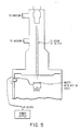
- FIG. 5 schematically represents the type of electron beam system which was used to alter the acceleration voltage of the electron beam used to image the polymeric resist material.
- the sensitized polymeric resist system used in combination with the low voltage electron beam system was comprised of poly(tert-butyloxycarbonyloxystyrene) in combination with a triphenylsulfonium hexafluoroarsenate sensitizer.
- the polymeric resist material was placed in a suitable solvent and applied to a semiconductor substrate using standard spin coating techniques.
- the surface of the applied resist was exposed to patterned radiation of net voltage of 3 Kev (main column at 20 Kev, and support structure for the resist structure at 17 Kev) using direct write techniques.
- Fig. 6 shows the absorbed energy density as a function of depth of penetration of the radiation into the resist, and as a function of the Kev net voltage.
- the irradiated resist structure was then heat treated for time periods ranging from about 30 seconds to about 180 seconds, at temperatures ranging from about 80°C to about 140°C, to insure chemical conversion of the irradiated upper portions of the resist layer to a chemical structure comprising phenolic hydroxyl functional groups.
- the resist structure was then placed in a vacuum oven, heated to temperatures ranging from about 100°C to about 150°C; the vacuum oven was evacuated. Subsequently the vacuum oven was filled with about 160 mbar (120 torr) of hexamethyldisilazane (HMDS). The HMDS was permitted to react with the hydroxyl functional groups in the irradiated areas of the upper portion of the polymeric resist material for a period of about 15 minutes.
- the resist structure was transferred from the vacuum oven to a commercially available oxygen reactive ion etching system, and the negative tone relief image was developed with 100 Watt Rf, at about 20 Sccm oxygen, at about 106 ⁇ bar (80 mtorr) for a period of about 12 minutes.
- This example demonstrates a method of creating a multilevel solvent-developable resist from a single layer of polymeric resist material.
- the polymeric resist material was comprised of poly (tert-butyloxycarbonyloxy-styrene) combined with a triphenylsulfonium hexafluoroantimonate sensitizer.
- the polymeric resist material was placed in a solvent and applied to a semiconductor substrate using spin coating techniques well known in the art, the generate about a 2 micrometer thick film on the semiconductor substrate.
- Fig. 5 depicts a cross-sectional view of the polymeric resist material 22 atop the silicon wafer substate 20 used for this particular example.
- the resist structure was exposed through a mask using a dosage of about 0.5 mJ/cm2 of 220 nm light to alter the sensitizer, thereby generating acid within the upper portions of the irradiated resist areas, as shown in Fig. 2.
- the acid was limited to the upper portions of the irradiated resist areas because the resist material absorbs strongly at the 220 nm light wavelength.
- the resist material was then heat treated at a temperature of about 100°C for a period of about 2 minutes to convert the upper portions of the irradiated areas of the polymeric resist layer 22 to a chemical structure comprising phenolic hydroxyl functional groups 24.
- the resist structure was then placed in a vacuum oven approximately one liter in size, at about 120°C and the vacuum oven chamber was evacuated. About 5 cc of triethylamine was injected into the vacuum oven chamber, and after about 5 minutes about 10 cc of phenyl isocyanate was also injected. The resist structure was exposed to the isocyanate for a period of about 10 minutes, after which the residual triethylamine and phenyl isocyanate vapors were pumped out of the vacuum oven. The amine was used to catalyze the reaction between the phenyl isocyanate and the functional hydroxyl groups of the polymeric resist material, and any equivalent organic base could have been used.
- the isocyanate can be any isocyanate capable of reacting with the phenolic hydroxyl to form a chromophore which has the necessary absorbance properties; however, phenyl isocyanate or a substituted phenyl isocyanate is preferred when the reactant is to be a gas phase reactant.
- the resist structure was heat treated for about 10 to about 15 minutes at about 130°C to about 135°C under reduced pressure ranging from about 0.133 to about 1.33 mbar (0.1 to about 1.0 torr), to remove any residual amine or isocyanate which is physically present on the resist surface but not reacted with the functional hydroxyl groups of the polymeric resist material. Reaction of the phenyl hydroxyl functional groups in the irradiated upper portions of the polymeric resist material with the triethylamine and phenyl isocyanate results in the formation of urethane in the upper portions of the irradiated areas 26, as shown in Fig. 3A.
- the structure yielded would have been that shown in Fig. 3B, wherein the non-irradiated areas 28 react to form the urethane.
- the urethane that was produced absorbs strongly in the 240 to 260 nm light wavelength at which the polymeric resist material was typically exposed in order chemically alter the sensitizer in the irradiated areas.
- the resist structure was then flood exposed at a dosage of about 100 mJ/cm2 with 254 nm light, and the exposed resist was heat treated at about 100°C for a period of about 2 minutes, to generate the phenolic hydroxyl functional groups which render it soluble in solvents such as isopropanol.
- the polymeric resist material underlying the upper portion of the resist layer which had been converted to the urethane is not soluble in the isopropanol since it was unaffected by the flood exposure at 254 nm light.
- the patterned resist was developed using isopropanol solvent and standard development techniques to produce the negative tone resist structure shown in Fig. 4A. Due to the use of isopropanol developer, the dyed upper portion of the resist 26 was not removed during development. It is not critical that the dyed portion of the resist remain after development, but may be advantageous in that the resultant resist structure is thicker. Had the reverse image structure of Fig. 3B been developed, the positive tone resist structure shown in Fig. 4B would have been generated.
- Fig. 7 is a photomicrograph showing the developed, top-imaged negative tone resist structure (in the form of 3 micrometer lines and spaces) obtained using the above method.
- one of the less preferred embodiments of the present invention is to use a transparent resist material and a penetrating source of radiation, and to obtain a top-imaged resist by controlling the process conditions during treatment of the resist with an organometallic reagent, a dye, or reagent capable of forming a dye upon reaction with the polymeric portion of the resist.
- a top-imaged etch-resistant resist structure has been prepared using this method, as described below:
- the polymeric resist material was comprised of poly (tert-butyloxycarbonyloxystyrene) in combination with a triphenylsulfonium hexafluoroantimonate sensitizer.
- the polymeric resist material was placed in a solvent and applied to a semiconductor substrate using spin coating techniques well known in the art, to generate about a 3 micrometer thick film on the semiconductor substrate.
- the resist film was exposed to patterned radiation about 250 nm in wavelength, at a dosage of about 10 mJ/cm2.
- the resist was then heat treated at around 100°C for about 2 minutes. This exposure and heat treatment liberated the phenolic groups through the entire film thickness in the patternwise-irradiated areas.
- Fig. 8,E shows the IR spectrum for the phenolic groups present in the resist film.
- HMDS hexamethyldisilazane
- HMDS treatment time The depth of penetration of the organometallic reagent HMDS into the resist film and the depth to which the film has been rendered etch resistant has, thus, been controlled by controlling HMDS treatment time.
- Another method of controlling depth of penetration/silylation of the resist thickness is to control the temperature during the HMDS treatment.
- Fig. 9 shows the extent of HMDS incorporation into a 1 micrometer thick resist film as a function of reaction time and temperature, as monitored by the increase in Si-O-Ph absorbance.
- Fig. 9, H shows the 120°C incorporation rate;
- Fig. 9, I shows the 110°C incorporation rate;
- Fig. 9, J shows the 100°C incorporation rate.
- Other process parameters such as pressure can be altered to affect the depth of penetration of the HMDS reagent.
- the same concept can be used to control the depth of penetration of a dye.
Landscapes
- Physics & Mathematics (AREA)
- General Physics & Mathematics (AREA)
- Spectroscopy & Molecular Physics (AREA)
- Chemical & Material Sciences (AREA)
- Chemical Kinetics & Catalysis (AREA)
- Inorganic Chemistry (AREA)
- Organic Chemistry (AREA)
- Photosensitive Polymer And Photoresist Processing (AREA)
- Materials For Photolithography (AREA)
- Exposure And Positioning Against Photoresist Photosensitive Materials (AREA)
- Exposure Of Semiconductors, Excluding Electron Or Ion Beam Exposure (AREA)
Applications Claiming Priority (2)
| Application Number | Priority Date | Filing Date | Title |
|---|---|---|---|
| US880212 | 1986-06-30 | ||
| US06/880,212 US4810601A (en) | 1984-12-07 | 1986-06-30 | Top imaged resists |
Publications (3)
| Publication Number | Publication Date |
|---|---|
| EP0251241A2 true EP0251241A2 (de) | 1988-01-07 |
| EP0251241A3 EP0251241A3 (en) | 1989-01-11 |
| EP0251241B1 EP0251241B1 (de) | 1991-09-18 |
Family
ID=25375739
Family Applications (1)
| Application Number | Title | Priority Date | Filing Date |
|---|---|---|---|
| EP87109212A Expired EP0251241B1 (de) | 1986-06-30 | 1987-06-26 | Oberflächig bebilderter Schutzlack |
Country Status (4)
| Country | Link |
|---|---|
| US (1) | US4810601A (de) |
| EP (1) | EP0251241B1 (de) |
| JP (1) | JPS6371843A (de) |
| DE (1) | DE3773061D1 (de) |
Cited By (7)
| Publication number | Priority date | Publication date | Assignee | Title |
|---|---|---|---|---|
| EP0394738A3 (de) * | 1989-04-24 | 1991-03-27 | Siemens Aktiengesellschaft | Vereinfachtes Mehrlagenphotoresistsystem |
| EP0282201A3 (de) * | 1987-03-09 | 1991-04-10 | Matsushita Electric Industrial Co., Ltd. | Verfahren zur Herstellung von Mustern |
| EP0453610A1 (de) * | 1990-04-27 | 1991-10-30 | Siemens Aktiengesellschaft | Verfahren zur Erzeugung einer Resiststruktur |
| EP0517428A1 (de) * | 1991-06-07 | 1992-12-09 | Shin-Etsu Chemical Co., Ltd. | Poly(para-t-butyloxycarbonyl-oxystyrol) und Verfahren zu seiner Herstellung |
| US5229258A (en) * | 1990-04-12 | 1993-07-20 | Siemens Aktiengesellschaft | Method for producing a resist structure |
| EP0600747A3 (de) * | 1992-12-04 | 1995-05-24 | Samsung Electronics Co Ltd | Verfahren und zur Herstellung von Feinstrukturen. |
| EP0785470A3 (de) * | 1996-01-16 | 2000-03-29 | Sumitomo Chemical Company, Limited | Verfahren zur Erzeugung eines Resistmusters |
Families Citing this family (37)
| Publication number | Priority date | Publication date | Assignee | Title |
|---|---|---|---|---|
| US5215867A (en) * | 1983-09-16 | 1993-06-01 | At&T Bell Laboratories | Method with gas functionalized plasma developed layer |
| US5064681A (en) * | 1986-08-21 | 1991-11-12 | International Business Machines Corporation | Selective deposition process for physical vapor deposition |
| JPH01186934A (ja) * | 1988-01-21 | 1989-07-26 | Toshiba Corp | パターン形成方法 |
| US5015559A (en) * | 1988-07-26 | 1991-05-14 | Matsushita Electric Industrial Co., Ltd. | Process for forming a fine resist pattern |
| US5079131A (en) * | 1988-08-29 | 1992-01-07 | Shipley Company Inc. | Method of forming positive images through organometallic treatment of negative acid hardening cross-linked photoresist formulations |
| US5094936A (en) * | 1988-09-16 | 1992-03-10 | Texas Instruments Incorporated | High pressure photoresist silylation process and apparatus |
| JPH0299960A (ja) * | 1988-10-06 | 1990-04-11 | Matsushita Electric Ind Co Ltd | パターン形成方法 |
| JP2737225B2 (ja) * | 1989-03-27 | 1998-04-08 | 松下電器産業株式会社 | 微細パターン形成材料およびパターン形成方法 |
| US5041362A (en) * | 1989-07-06 | 1991-08-20 | Texas Instruments Incorporated | Dry developable resist etch chemistry |
| US4981770A (en) * | 1989-07-28 | 1991-01-01 | At&T Bell Laboratories | Process for fabrication of device |
| US5217851A (en) * | 1989-09-05 | 1993-06-08 | Mitsubishi Denki Kabushiki Kaisha | Pattern forming method capable of providing an excellent pattern of high resolution power and high sensitivity |
| US5362606A (en) * | 1989-10-18 | 1994-11-08 | Massachusetts Institute Of Technology | Positive resist pattern formation through focused ion beam exposure and surface barrier silylation |
| US5139925A (en) * | 1989-10-18 | 1992-08-18 | Massachusetts Institute Of Technology | Surface barrier silylation of novolak film without photoactive additive patterned with 193 nm excimer laser |
| US5023164A (en) * | 1989-10-23 | 1991-06-11 | International Business Machines Corporation | Highly sensitive dry developable deep UV photoresist |
| US5128223A (en) * | 1990-06-15 | 1992-07-07 | Hoechst Celanese Corp. | Polymeric direct imaging holographic compositions |
| US5824455A (en) * | 1990-09-26 | 1998-10-20 | Canon Kabushiki Kaisha | Processing method and apparatus |
| EP0909988A1 (de) * | 1990-09-26 | 1999-04-21 | Canon Kabushiki Kaisha | Photolithographisches Verarbeitungsverfahren |
| US5250395A (en) * | 1991-07-25 | 1993-10-05 | International Business Machines Corporation | Process for imaging of photoresist including treatment of the photoresist with an organometallic compound |
| DE69208769T2 (de) * | 1991-07-31 | 1996-07-18 | Texas Instruments Inc | Hochauflösendes lithographisches Verfahren |
| US5296332A (en) * | 1991-11-22 | 1994-03-22 | International Business Machines Corporation | Crosslinkable aqueous developable photoresist compositions and method for use thereof |
| US5322765A (en) * | 1991-11-22 | 1994-06-21 | International Business Machines Corporation | Dry developable photoresist compositions and method for use thereof |
| US5229256A (en) * | 1991-12-06 | 1993-07-20 | International Business Machines Corporation | Process for generating positive-tone photoresist image |
| US5286607A (en) * | 1991-12-09 | 1994-02-15 | Chartered Semiconductor Manufacturing Pte Ltd. | Bi-layer resist process for semiconductor processing |
| JP2951504B2 (ja) * | 1992-06-05 | 1999-09-20 | シャープ株式会社 | シリル化平坦化レジスト及び平坦化方法並びに集積回路デバイスの製造方法 |
| US5312717A (en) * | 1992-09-24 | 1994-05-17 | International Business Machines Corporation | Residue free vertical pattern transfer with top surface imaging resists |
| US5352330A (en) * | 1992-09-30 | 1994-10-04 | Texas Instruments Incorporated | Process for producing nanometer-size structures on surfaces using electron beam induced chemistry through electron stimulated desorption |
| JP2654339B2 (ja) * | 1992-11-24 | 1997-09-17 | インターナショナル・ビジネス・マシーンズ・コーポレイション | 感光性レジスト組成物及び基板上にレジスト像を形成する方法 |
| US5460693A (en) * | 1994-05-31 | 1995-10-24 | Texas Instruments Incorporated | Dry microlithography process |
| JP3389754B2 (ja) * | 1994-11-14 | 2003-03-24 | 松下電器産業株式会社 | 化学吸着膜の形成方法 |
| US5702869A (en) * | 1996-06-07 | 1997-12-30 | Vanguard International Semiconductor Corporation | Soft ashing method for removing fluorinated photoresists layers from semiconductor substrates |
| US6764808B2 (en) * | 2002-02-27 | 2004-07-20 | Advanced Micro Devices, Inc. | Self-aligned pattern formation using wavelenghts |
| US7270940B2 (en) * | 2002-12-18 | 2007-09-18 | International Business Machines Corporation | Method of structuring of a substrate |
| JP2006013216A (ja) * | 2004-06-28 | 2006-01-12 | Canon Inc | 近接場露光によるレジストパターンの形成方法、及び該レジストパターンの形成方法を用いた基板の加工方法、デバイスの作製方法 |
| US7977253B2 (en) * | 2004-08-31 | 2011-07-12 | Semiconductor Energy Laboratory Co., Ltd. | Manufacturing method of semiconductor device |
| US8557647B2 (en) | 2011-09-09 | 2013-10-15 | International Business Machines Corporation | Method for fabricating field effect transistor devices with high-aspect ratio mask |
| JP6465189B2 (ja) * | 2016-07-21 | 2019-02-06 | 東京エレクトロン株式会社 | 半導体装置の製造方法及び真空処理装置 |
| TWI753105B (zh) * | 2017-02-22 | 2022-01-21 | 日商信越化學工業股份有限公司 | 圖型形成方法 |
Family Cites Families (16)
| Publication number | Priority date | Publication date | Assignee | Title |
|---|---|---|---|---|
| JPS5635130A (en) * | 1979-08-31 | 1981-04-07 | Fujitsu Ltd | Resist material and method for forming resist pattern |
| US4508813A (en) * | 1980-06-16 | 1985-04-02 | Fujitsu Limited | Method for producing negative resist images |
| JPS5844715A (ja) * | 1981-09-11 | 1983-03-15 | Fujitsu Ltd | 微細パタ−ン形成方法 |
| US4357369A (en) * | 1981-11-10 | 1982-11-02 | Rca Corporation | Method of plasma etching a substrate |
| DE3151078A1 (de) * | 1981-12-23 | 1983-07-28 | Hoechst Ag, 6230 Frankfurt | Verfahren zur herstellung von reliefbildern |
| EP0091651B1 (de) * | 1982-04-12 | 1988-08-03 | Nippon Telegraph And Telephone Corporation | Verfahren zur Herstellung von Mikrobildern |
| GB2121197A (en) * | 1982-05-26 | 1983-12-14 | Philips Electronic Associated | Plasma-etch resistant mask formation |
| DE3231145A1 (de) * | 1982-08-21 | 1984-02-23 | Basf Ag, 6700 Ludwigshafen | Negativ arbeitendes verfahren zur herstellung von reliefbildern oder resistmustern |
| US4433044A (en) * | 1982-11-15 | 1984-02-21 | Rca Corporation | Dry developable positive photoresists |
| US4430153A (en) * | 1983-06-30 | 1984-02-07 | International Business Machines Corporation | Method of forming an RIE etch barrier by in situ conversion of a silicon containing alkyl polyamide/polyimide |
| GB8403698D0 (en) * | 1984-02-13 | 1984-03-14 | British Telecomm | Semiconductor device fabrication |
| US4552833A (en) * | 1984-05-14 | 1985-11-12 | International Business Machines Corporation | Radiation sensitive and oxygen plasma developable resist |
| US4543270A (en) * | 1984-06-20 | 1985-09-24 | Gould Inc. | Method for depositing a micron-size metallic film on a transparent substrate utilizing a visible laser |
| GB8427149D0 (en) * | 1984-10-26 | 1984-12-05 | Ucb Sa | Resist materials |
| CA1267378A (en) * | 1984-12-07 | 1990-04-03 | Jer-Ming Yang | Top imaged and organosilicon treated polymer layer developable with plasma |
| US4613398A (en) * | 1985-06-06 | 1986-09-23 | International Business Machines Corporation | Formation of etch-resistant resists through preferential permeation |
-
1986
- 1986-06-30 US US06/880,212 patent/US4810601A/en not_active Expired - Lifetime
-
1987
- 1987-05-18 JP JP62119155A patent/JPS6371843A/ja active Pending
- 1987-06-26 DE DE8787109212T patent/DE3773061D1/de not_active Expired - Lifetime
- 1987-06-26 EP EP87109212A patent/EP0251241B1/de not_active Expired
Cited By (9)
| Publication number | Priority date | Publication date | Assignee | Title |
|---|---|---|---|---|
| EP0282201A3 (de) * | 1987-03-09 | 1991-04-10 | Matsushita Electric Industrial Co., Ltd. | Verfahren zur Herstellung von Mustern |
| EP0394738A3 (de) * | 1989-04-24 | 1991-03-27 | Siemens Aktiengesellschaft | Vereinfachtes Mehrlagenphotoresistsystem |
| US5229258A (en) * | 1990-04-12 | 1993-07-20 | Siemens Aktiengesellschaft | Method for producing a resist structure |
| EP0453610A1 (de) * | 1990-04-27 | 1991-10-30 | Siemens Aktiengesellschaft | Verfahren zur Erzeugung einer Resiststruktur |
| US5262283A (en) * | 1990-04-27 | 1993-11-16 | Siemens Aktiengesellschaft | Method for producing a resist structure |
| EP0517428A1 (de) * | 1991-06-07 | 1992-12-09 | Shin-Etsu Chemical Co., Ltd. | Poly(para-t-butyloxycarbonyl-oxystyrol) und Verfahren zu seiner Herstellung |
| US5523370A (en) * | 1991-06-07 | 1996-06-04 | Shin-Etsu Chemical Co., Ltd. | Poly(para-T-butoxycarbonyloxystyrene) and method of making |
| EP0600747A3 (de) * | 1992-12-04 | 1995-05-24 | Samsung Electronics Co Ltd | Verfahren und zur Herstellung von Feinstrukturen. |
| EP0785470A3 (de) * | 1996-01-16 | 2000-03-29 | Sumitomo Chemical Company, Limited | Verfahren zur Erzeugung eines Resistmusters |
Also Published As
| Publication number | Publication date |
|---|---|
| US4810601A (en) | 1989-03-07 |
| JPS6371843A (ja) | 1988-04-01 |
| EP0251241A3 (en) | 1989-01-11 |
| DE3773061D1 (de) | 1991-10-24 |
| EP0251241B1 (de) | 1991-09-18 |
Similar Documents
| Publication | Publication Date | Title |
|---|---|---|
| EP0251241B1 (de) | Oberflächig bebilderter Schutzlack | |
| US5366851A (en) | Device fabrication process | |
| US4908298A (en) | Method of creating patterned multilayer films for use in production of semiconductor circuits and systems | |
| KR100573672B1 (ko) | 레지스트 구조물의 형성 방법 | |
| TW573213B (en) | Photoresist composition for deep UV radiation | |
| US5240812A (en) | Top coat for acid catalyzed resists | |
| US20040152024A1 (en) | Method for modifying resist images by electron beam exposure | |
| US6258514B1 (en) | Top surface imaging technique using a topcoat delivery system | |
| KR100576926B1 (ko) | 화학적으로강화된레지스트 | |
| US6632582B2 (en) | Pattern formation material and pattern formation method | |
| EP0195291B1 (de) | Verfahren zur Bildung von Reliefstrukturen enthaltenden Mehrschichtfilmen für die Herstellung von Halbleiterschaltkreisen und -systemen | |
| EP0186798B1 (de) | Plasmaentwickelfähige Schutzlacke mit Oberflächenbild | |
| EP0285025A2 (de) | Silylierte Phenolharze | |
| US6989227B2 (en) | E-beam curable resist and process for e-beam curing the resist | |
| US6475706B1 (en) | Pattern formation method | |
| EP0515079B1 (de) | Resistmaterialien und Verfahren zur Verwendung | |
| EP0250762B1 (de) | Herstellung von permeabelen polymeren Filmen oder Schichten durch Auslaugung | |
| JPH0143300B2 (de) | ||
| EP1789850B1 (de) | Neuartiges resistmaterial und verfahren zur bildung einer strukturierten resistschicht auf einem substrat | |
| EP0366937A2 (de) | Verfahren zur Herstellung von Reliefstrukturen und Anwendung | |
| EP1148388A1 (de) | Material und Verfahren zur Herstellung von Mustern | |
| JP3307709B2 (ja) | レジストパターンの形成方法 | |
| JPH07104483A (ja) | パターンの形成方法 | |
| JPH06267812A (ja) | 微細パターン形成材料およびパターン形成方法 | |
| KR19980014987A (ko) | 원자외선용 감광막과 반도체소자의 미세패턴 형성방법 |
Legal Events
| Date | Code | Title | Description |
|---|---|---|---|
| PUAI | Public reference made under article 153(3) epc to a published international application that has entered the european phase |
Free format text: ORIGINAL CODE: 0009012 |
|
| AK | Designated contracting states |
Kind code of ref document: A2 Designated state(s): DE FR GB IT |
|
| 17P | Request for examination filed |
Effective date: 19880426 |
|
| PUAL | Search report despatched |
Free format text: ORIGINAL CODE: 0009013 |
|
| AK | Designated contracting states |
Kind code of ref document: A3 Designated state(s): DE FR GB IT |
|
| 17Q | First examination report despatched |
Effective date: 19890907 |
|
| GRAA | (expected) grant |
Free format text: ORIGINAL CODE: 0009210 |
|
| AK | Designated contracting states |
Kind code of ref document: B1 Designated state(s): DE FR GB IT |
|
| PG25 | Lapsed in a contracting state [announced via postgrant information from national office to epo] |
Ref country code: IT Free format text: LAPSE BECAUSE OF FAILURE TO SUBMIT A TRANSLATION OF THE DESCRIPTION OR TO PAY THE FEE WITHIN THE PRESCRIBED TIME-LIMIT;WARNING: LAPSES OF ITALIAN PATENTS WITH EFFECTIVE DATE BEFORE 2007 MAY HAVE OCCURRED AT ANY TIME BEFORE 2007. THE CORRECT EFFECTIVE DATE MAY BE DIFFERENT FROM THE ONE RECORDED. Effective date: 19910918 |
|
| REF | Corresponds to: |
Ref document number: 3773061 Country of ref document: DE Date of ref document: 19911024 |
|
| ET | Fr: translation filed | ||
| PLBE | No opposition filed within time limit |
Free format text: ORIGINAL CODE: 0009261 |
|
| STAA | Information on the status of an ep patent application or granted ep patent |
Free format text: STATUS: NO OPPOSITION FILED WITHIN TIME LIMIT |
|
| 26N | No opposition filed | ||
| PGFP | Annual fee paid to national office [announced via postgrant information from national office to epo] |
Ref country code: GB Payment date: 19960520 Year of fee payment: 10 |
|
| PGFP | Annual fee paid to national office [announced via postgrant information from national office to epo] |
Ref country code: FR Payment date: 19960607 Year of fee payment: 10 |
|
| PG25 | Lapsed in a contracting state [announced via postgrant information from national office to epo] |
Ref country code: GB Free format text: LAPSE BECAUSE OF NON-PAYMENT OF DUE FEES Effective date: 19970626 |
|
| GBPC | Gb: european patent ceased through non-payment of renewal fee |
Effective date: 19970626 |
|
| PG25 | Lapsed in a contracting state [announced via postgrant information from national office to epo] |
Ref country code: FR Free format text: LAPSE BECAUSE OF NON-PAYMENT OF DUE FEES Effective date: 19980227 |
|
| REG | Reference to a national code |
Ref country code: FR Ref legal event code: ST |
|
| REG | Reference to a national code |
Ref country code: FR Ref legal event code: ST |
|
| PGFP | Annual fee paid to national office [announced via postgrant information from national office to epo] |
Ref country code: DE Payment date: 19990622 Year of fee payment: 13 |
|
| PG25 | Lapsed in a contracting state [announced via postgrant information from national office to epo] |
Ref country code: DE Free format text: LAPSE BECAUSE OF NON-PAYMENT OF DUE FEES Effective date: 20010403 |