EP0186798B1 - Plasmaentwickelfähige Schutzlacke mit Oberflächenbild - Google Patents
Plasmaentwickelfähige Schutzlacke mit Oberflächenbild Download PDFInfo
- Publication number
- EP0186798B1 EP0186798B1 EP19850115321 EP85115321A EP0186798B1 EP 0186798 B1 EP0186798 B1 EP 0186798B1 EP 19850115321 EP19850115321 EP 19850115321 EP 85115321 A EP85115321 A EP 85115321A EP 0186798 B1 EP0186798 B1 EP 0186798B1
- Authority
- EP
- European Patent Office
- Prior art keywords
- layer
- polymeric material
- upper portion
- ranges
- irradiated
- Prior art date
- Legal status (The legal status is an assumption and is not a legal conclusion. Google has not performed a legal analysis and makes no representation as to the accuracy of the status listed.)
- Expired
Links
- 239000000463 material Substances 0.000 claims description 37
- 238000000034 method Methods 0.000 claims description 37
- 239000003153 chemical reaction reagent Substances 0.000 claims description 16
- 229920000642 polymer Polymers 0.000 claims description 16
- 125000002524 organometallic group Chemical group 0.000 claims description 14
- 230000005855 radiation Effects 0.000 claims description 14
- 125000004435 hydrogen atom Chemical group [H]* 0.000 claims description 13
- 125000001997 phenyl group Chemical group [H]C1=C([H])C([H])=C(*)C([H])=C1[H] 0.000 claims description 13
- QVGXLLKOCUKJST-UHFFFAOYSA-N atomic oxygen Chemical compound [O] QVGXLLKOCUKJST-UHFFFAOYSA-N 0.000 claims description 10
- 239000001301 oxygen Substances 0.000 claims description 10
- 229910052760 oxygen Inorganic materials 0.000 claims description 10
- 239000000758 substrate Substances 0.000 claims description 10
- 230000008707 rearrangement Effects 0.000 claims description 9
- 125000000217 alkyl group Chemical group 0.000 claims description 4
- 125000003118 aryl group Chemical group 0.000 claims description 4
- -1 o-nitrobenzyl Chemical class 0.000 claims description 4
- 239000002253 acid Substances 0.000 claims description 3
- 150000007513 acids Chemical class 0.000 claims description 3
- 150000001298 alcohols Chemical class 0.000 claims description 3
- 150000001412 amines Chemical class 0.000 claims description 3
- 239000007795 chemical reaction product Substances 0.000 claims description 3
- 239000000203 mixture Substances 0.000 claims description 3
- 206010073306 Exposure to radiation Diseases 0.000 claims description 2
- 238000010894 electron beam technology Methods 0.000 claims description 2
- 238000010884 ion-beam technique Methods 0.000 claims description 2
- 230000001678 irradiating effect Effects 0.000 claims description 2
- NIXOWILDQLNWCW-UHFFFAOYSA-M Acrylate Chemical compound [O-]C(=O)C=C NIXOWILDQLNWCW-UHFFFAOYSA-M 0.000 claims 1
- 230000015572 biosynthetic process Effects 0.000 claims 1
- 229910010272 inorganic material Inorganic materials 0.000 claims 1
- 239000011147 inorganic material Substances 0.000 claims 1
- 239000002210 silicon-based material Substances 0.000 claims 1
- 125000003011 styrenyl group Chemical class [H]\C(*)=C(/[H])C1=C([H])C([H])=C([H])C([H])=C1[H] 0.000 claims 1
- 239000010410 layer Substances 0.000 description 47
- 230000008569 process Effects 0.000 description 13
- 150000001875 compounds Chemical class 0.000 description 8
- FFUAGWLWBBFQJT-UHFFFAOYSA-N hexamethyldisilazane Chemical compound C[Si](C)(C)N[Si](C)(C)C FFUAGWLWBBFQJT-UHFFFAOYSA-N 0.000 description 8
- 229920001665 Poly-4-vinylphenol Polymers 0.000 description 6
- 238000006243 chemical reaction Methods 0.000 description 5
- XUIMIQQOPSSXEZ-UHFFFAOYSA-N Silicon Chemical compound [Si] XUIMIQQOPSSXEZ-UHFFFAOYSA-N 0.000 description 3
- 238000007306 functionalization reaction Methods 0.000 description 3
- 238000004519 manufacturing process Methods 0.000 description 3
- 238000001393 microlithography Methods 0.000 description 3
- 229920002120 photoresistant polymer Polymers 0.000 description 3
- 239000013047 polymeric layer Substances 0.000 description 3
- 229910052710 silicon Inorganic materials 0.000 description 3
- 239000010703 silicon Substances 0.000 description 3
- ZGHFDIIVVIFNPS-UHFFFAOYSA-N 3-Methyl-3-buten-2-one Chemical compound CC(=C)C(C)=O ZGHFDIIVVIFNPS-UHFFFAOYSA-N 0.000 description 2
- UFHFLCQGNIYNRP-UHFFFAOYSA-N Hydrogen Chemical compound [H][H] UFHFLCQGNIYNRP-UHFFFAOYSA-N 0.000 description 2
- VYPSYNLAJGMNEJ-UHFFFAOYSA-N Silicium dioxide Chemical compound O=[Si]=O VYPSYNLAJGMNEJ-UHFFFAOYSA-N 0.000 description 2
- SBZXBUIDTXKZTM-UHFFFAOYSA-N diglyme Chemical compound COCCOCCOC SBZXBUIDTXKZTM-UHFFFAOYSA-N 0.000 description 2
- 239000007789 gas Substances 0.000 description 2
- 239000001257 hydrogen Substances 0.000 description 2
- 229910052739 hydrogen Inorganic materials 0.000 description 2
- 229920003229 poly(methyl methacrylate) Polymers 0.000 description 2
- 239000004926 polymethyl methacrylate Substances 0.000 description 2
- 239000000047 product Substances 0.000 description 2
- 229910052814 silicon oxide Inorganic materials 0.000 description 2
- 239000002904 solvent Substances 0.000 description 2
- KXGFMDJXCMQABM-UHFFFAOYSA-N 2-methoxy-6-methylphenol Chemical compound [CH]OC1=CC=CC([CH])=C1O KXGFMDJXCMQABM-UHFFFAOYSA-N 0.000 description 1
- CMWKITSNTDAEDT-UHFFFAOYSA-N 2-nitrobenzaldehyde Chemical class [O-][N+](=O)C1=CC=CC=C1C=O CMWKITSNTDAEDT-UHFFFAOYSA-N 0.000 description 1
- 238000005618 Fries rearrangement reaction Methods 0.000 description 1
- 239000004793 Polystyrene Substances 0.000 description 1
- 229910003910 SiCl4 Inorganic materials 0.000 description 1
- 238000004380 ashing Methods 0.000 description 1
- 150000001540 azides Chemical class 0.000 description 1
- 230000004888 barrier function Effects 0.000 description 1
- SRSXLGNVWSONIS-UHFFFAOYSA-N benzenesulfonic acid Chemical compound OS(=O)(=O)C1=CC=CC=C1 SRSXLGNVWSONIS-UHFFFAOYSA-N 0.000 description 1
- 229940092714 benzenesulfonic acid Drugs 0.000 description 1
- 239000011248 coating agent Substances 0.000 description 1
- 238000000576 coating method Methods 0.000 description 1
- 238000010668 complexation reaction Methods 0.000 description 1
- 238000001312 dry etching Methods 0.000 description 1
- 229920001971 elastomer Polymers 0.000 description 1
- 238000003384 imaging method Methods 0.000 description 1
- 229910001502 inorganic halide Inorganic materials 0.000 description 1
- LQNUZADURLCDLV-UHFFFAOYSA-N nitrobenzene Chemical class [O-][N+](=O)C1=CC=CC=C1 LQNUZADURLCDLV-UHFFFAOYSA-N 0.000 description 1
- 230000035515 penetration Effects 0.000 description 1
- 229920001568 phenolic resin Polymers 0.000 description 1
- 239000005011 phenolic resin Substances 0.000 description 1
- 150000002989 phenols Chemical class 0.000 description 1
- 238000001020 plasma etching Methods 0.000 description 1
- 229920002223 polystyrene Polymers 0.000 description 1
- 239000005060 rubber Substances 0.000 description 1
- FDNAPBUWERUEDA-UHFFFAOYSA-N silicon tetrachloride Chemical compound Cl[Si](Cl)(Cl)Cl FDNAPBUWERUEDA-UHFFFAOYSA-N 0.000 description 1
- 238000006884 silylation reaction Methods 0.000 description 1
- 239000002356 single layer Substances 0.000 description 1
- 239000007787 solid Substances 0.000 description 1
- 238000004528 spin coating Methods 0.000 description 1
- 238000009281 ultraviolet germicidal irradiation Methods 0.000 description 1
Images
Classifications
-
- G—PHYSICS
- G03—PHOTOGRAPHY; CINEMATOGRAPHY; ANALOGOUS TECHNIQUES USING WAVES OTHER THAN OPTICAL WAVES; ELECTROGRAPHY; HOLOGRAPHY
- G03F—PHOTOMECHANICAL PRODUCTION OF TEXTURED OR PATTERNED SURFACES, e.g. FOR PRINTING, FOR PROCESSING OF SEMICONDUCTOR DEVICES; MATERIALS THEREFOR; ORIGINALS THEREFOR; APPARATUS SPECIALLY ADAPTED THEREFOR
- G03F7/00—Photomechanical, e.g. photolithographic, production of textured or patterned surfaces, e.g. printing surfaces; Materials therefor, e.g. comprising photoresists; Apparatus specially adapted therefor
- G03F7/26—Processing photosensitive materials; Apparatus therefor
- G03F7/265—Selective reaction with inorganic or organometallic reagents after image-wise exposure, e.g. silylation
-
- G—PHYSICS
- G03—PHOTOGRAPHY; CINEMATOGRAPHY; ANALOGOUS TECHNIQUES USING WAVES OTHER THAN OPTICAL WAVES; ELECTROGRAPHY; HOLOGRAPHY
- G03F—PHOTOMECHANICAL PRODUCTION OF TEXTURED OR PATTERNED SURFACES, e.g. FOR PRINTING, FOR PROCESSING OF SEMICONDUCTOR DEVICES; MATERIALS THEREFOR; ORIGINALS THEREFOR; APPARATUS SPECIALLY ADAPTED THEREFOR
- G03F7/00—Photomechanical, e.g. photolithographic, production of textured or patterned surfaces, e.g. printing surfaces; Materials therefor, e.g. comprising photoresists; Apparatus specially adapted therefor
- G03F7/004—Photosensitive materials
- G03F7/038—Macromolecular compounds which are rendered insoluble or differentially wettable
Definitions
- the present invention is concerned with a method of converting the upper portion of a layer of polymeric material into a dry-etch resistant form.
- the method can be used to produce multi-layer, plasma-developable resists which are capable of providing submicron resolution.
- EP-A-0 184 567 relates to a process for forming a negative tone image with photoresist layers consisting of a photosensitive compound mixed with or attached to a polymer compound.
- the photosensitive compound is a diazoquinone, preferably a diazo-dihydro-oxo-1-naphthalene or benzene sulfonic acid.
- the polymeric compound is a phenolic resin. Therefore, this prior art reference cannot be regarded as relevant prior art reference with respect to the individual compounds (1) to (3) of claim 1 of the present invention.
- Solid State Technology, Vol. 27, No. 2, Feb. 1984, pp. 145-55 relates to a gas phase functionalization process of a resist with groups A or of the same resist with product groups P upon UV-irradiation.
- Gas phase functionalization of either A or P by inorganic reagent results in positive or negative tone pattern. Again this process bears no relation to the process of the present invention and the compounds used therein.
- the object of the present invention is a process which reduces the number of resist layer applications required to obtain high resolution submicron electronic component features while simultaneously providing for dry development. Such a process is particularly useful in the manufacture of electronic components.
- the lithographic process can utilize either high-absorptivity radiation-sensitive polymers which can be top imaged upon exposure to a radiation source or more transparent radition-sensitive polymers and carefully controlled conditions in subsequent process steps.
- radiation should be interpreted to include both photon (ultraviolet light from 150 nm - 600 nm and radiation emission sources such as electron beam, ion beam, and X-ray.
- a layer of high-absorptivity polymeric material is exposed to radiation which creates reactive hydrogens within the upper portion of the layer by moleculare rearrangement within the irradiated area.
- the reactive hydrogens are subsequently reacted with an organometallic reagent to form an etch barrier within the upper portion of the layer.
- the layer of polymeric resist is exposed to patterned radiation which creates the labile and reactive hydrogens within the upper portion of the layer in the pattern-wise irradiated areas.
- Irradiation is followed by treatment with an organometallic reagent to create the etch-resistant upper portion of the layer in the pattern-wise irradiated areas.
- Subsequent development of the resist image using dry development methods such as oxygen plasma produces at least a two-layer resist pattern with high aspect ratio and straight walls or under cut profiles, depending on etch conditions utilized.
- a resist pattern with more than two layers can be obtained by applying the polymeric resist to be imaged over other layers of polymeric resist material.
- the other layers of polymeric resist material need not be sensitive to radiation.
- An additional step can be used to dry develop the two layer resist, comprising:
- a less preferred embodiment utilizes a more transparent, radiation-sensitive polymer, wherein irradiation may penetrate up to the entire layer thickness.
- process conditions must be carefully controlled during the reaction with the organometallic reagent.
- the penetration of the organometallic reagent must be limited to the portion of the layer which is to become etch resistant.
- Embodiments of the present invention provide that the layer of polymeric material ranges from about 0.5 micrometer to about 20 micrometers in thickness, and that the upper portion of the layer which undergoes reaction with the organometallic reagent ranges from about 0.1 to 1.0 micrometer in depth.
- Preferred embodiments of the present invention provide that the layer of polymeric material ranges from about 1 to about 3 microns in thickness, and that the upper portion which undergoes reaction with the organometallic reagent ranges from about 0.1 to about 0.5 micrometers in depth.
- the method of the present invention reduces the number of resist layer applications required to obtain high resolution submicron electronic component features while simultaneously providing for dry development of the resist image.
- the polymeric material used to create the top-imaged two-layer resist may be comprised of a number of different materials, so long as labile and reactive hydrogens are created upon irradiation.
- R1, R2, R3, and R5 H, alkyl, aryl, or part of a polymer backbone
- R4 H, C n H 2n+1 where n ranges from 1 to about 5, phenyl or substituted phenyls.
- Materials of this type can be used alone or in combination with compatible polymeric materials.
- Compounds such as substituted o-nitrobenzaldehyde and esterified phenols can be mixed together with polymers which have no labile or reactive hydrogens, e.g., PMMA (poly methyl methacrylate), rubbers, PMIPK (poly methylisopropenyl ketone), and polystyrene and its derivatives.
- PMMA poly methyl methacrylate
- PMIPK poly methylisopropenyl ketone
- polystyrene and its derivatives Upon irradiation, the molecules which are sensitive to the radiation undergo rearrangement in the penetrated portion of the irradiated area of the polymeric layer, to yield products with labile and reactive hydrogens.
- the labile and reactive hydrogens can be subsequently reacted with an organometallic reagent to create the top-imaged resist.
- the solution was applied to a silicon oxide substrate using standard spin coating techniques. After application of the solution coating, the coated substrate was dried at about 80°C on a hotplate, to remove the diglyme solvent.
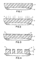
- Fig. 1 is a cross-sectional view of the polymeric resist material (acetylated polyvinylphenol) layer 12 atop the silicon oxide substrate 10. The thickness of the dried acetylated polyvinylphenol layer 12 was about 0.7 micrometers.
- Fig. 2 shows the same cross-sectional view after irradiation, wherein the irradiated areas 14 have experienced molecular rearrangement during which labile and reactive hydrogen sites have been created. Subsequently, the irradiated polymeric layer was exposed to HMDS (hexamethyldisilazane) vapor in order to silylate the active hydrogens created during the irradiation.
- HMDS hexamethyldisilazane
- FIG. 3 shows the cross-sectional view after treatment of the irradiated polymeric resist material with HMDS, so that a sylicated dry-etch-resistant form of material 16 was created in the upper portion of the irradiated areas.
- a good silylated image 16 formed within approximately 40 to 50 minutes after application of the HMDS reagent to the irradiated areas.
- the silylation reaction was followed by treatment of the structure described above with oxygen plasma at about 1.33 mbar and 0.3 Watts/cm2 for a period of about 6 minutes.
- the resultant two layer resist structure 18 was comprised of a silylated upper layer approximately 0.3 micrometers thick and a lower layer of acetylated polyvinylphenol about 0.4 micrometers thick, as depicted in Fig. 4. Note that treatment of an equivalent layer of unreacted polyvinylphenol with oxygen plasma under the same conditions results in ashing of the layer within about 4 to 5 minutes.
- the two-layer resist formed using the above process exhibited line widths of about one micrometer wherein the line sidewalls showed negligible undercutting upon oxygen plasma development.
Landscapes
- Physics & Mathematics (AREA)
- General Physics & Mathematics (AREA)
- Chemical & Material Sciences (AREA)
- Chemical Kinetics & Catalysis (AREA)
- Inorganic Chemistry (AREA)
- Organic Chemistry (AREA)
- Spectroscopy & Molecular Physics (AREA)
- Photosensitive Polymer And Photoresist Processing (AREA)
- Exposure And Positioning Against Photoresist Photosensitive Materials (AREA)
- Materials For Photolithography (AREA)
Claims (13)
- Verfahren zum Überführen des oberen Teils (16) einer Schicht polymeren Materials (12) in eine trockenätzbeständige Form, das folgende Verfahrensschritte umfaßt:
a) Aufbringen einer Schicht polymeren Materials (12) auf ein Substrat (10), wobei das Substrat mindestens eine Verbindung enthält, bei der bei Bestrahlung eine molekulare Umlagerung erfolgt, so daß labiler und reaktiver Wasserstoff freigesetzt wird und die aus der folgenden Gruppe von Verbindungen ausgewählt wird: (1) o-Nitrobenzyl-Derivate, die sich bei Bestrahlung in Alkohole, Säuren und Amine umlagern, (2) Gruppen, in denen eine photochemische Fries-Umlagerung erfolgen kann und (3) Mischungen beider;b) Musterförmige Bestrahlung von Teilen der Oberfläche (14) des polymeren Materials, um eine molekulare Umlagerung der Verbindung und die Freisetzung von labilem und reaktivem Wasserstoff zumindest in dem oberen Teil (16) der musterförmig bestrahlten Schicht zu erzielen; undc) Behandlung der Reaktionsprodukte in der bestrahlten Schicht mit einer reaktiven organometallischen Verbindung, um die organometallische Verbindung mit den reaktiven Zentren im oberen Teil (16) der Schicht polymeren Materials reagieren und eine Verbindung eingehen zu lassen, wobei die obere Schicht trockenätzbeständig wird. - Verfahren nach Anspruch 1, wobei die in dem polymeren Material enthaltene Verbindung aus der folgenden Gruppe von Verbindungen ausgewählt ist:

- Verfahren nach Anspruch 2, wobei R₁ Teil einer polymeren Hauptkette ist, die ein Styrolderivat oder ein Polymer auf Akrylatbasis ist, R₂, R₃, R₅ = H, CnH2n+1 wobei n von 1 bis etwa 15 läuft, Phenyl, substituierte Phenyle, und andere Radikale, die Benzolderivate sind, und R₄ = H, CnH2n+1 wobei n von 1 bis etwa 5 läuft, Phenyl und substituierte Phenyle.
- Verfahren nach Anspruch 1, wobei die Strahlenquelle aus der folgenden Gruppe ausgewählt wird: Photonemissionsquellen, Elektronenstrahl, Ionenstrahl- und Röntgenstrahlquellen.
- Verfahren nach Anspruch 1, wobei ein weiterer Verfahrensschritt vorliegt:
a) Entwicklung des musterförmigen Bildes auf den bestrahlten (14) und reagierten (16) Gebieten durch Behandlung mit einem Sauerstoffplasma. - Verfahren nach Anspruch 1, wobei die Dicke der Schicht aus polymerem Material zwischen etwa 0.5 und etwa 20 µm beträgt.
- Verfahren nach Anspruch 6, wobei die Dicke der Schicht aus polymerem Material zwischen etwa 1.0 und etwa 3.0 µm beträgt.
- Verfahren nach Anspruch 1, wobei die Dicke des durchstrahlten oberen Teils der musterförmig bestrahlten Gebiete der Schicht aus polymerem Material zwischen etwa 0.1 und etwa 1 µm beträgt.
- Verfahren nach Anspruch 8, wobei die Dicke des durchstrahlten oberen Teils der musterförmig bestrahlten Gebiete der Schicht aus polymerem Material zwischen etwa 0.1 und etwa 0.5 µm beträgt.
- Verfahren nach Anspruch 8, wobei die molekulare Umlagerung der zumindest einen Verbindung weitgehend in dem oberen Teil der Schicht aus polymerem Material stattfindet.
- Verfahren nach Anspruch 8, wobei die reaktive organometallische Verbindung eine siliziumhaltige Verbindung ist.
- Verfahren nach Anspruch 1, wobei das Substrat (10) ein polymeres Material enthält, das entweder strahlungsempfindlich oder nicht strahlungsempfindlich ist.
- Verfahren nach Anspruch 1, wobei das Substrat (10) ein anorganisches Material enthält.
Applications Claiming Priority (2)
| Application Number | Priority Date | Filing Date | Title |
|---|---|---|---|
| US67952784A | 1984-12-07 | 1984-12-07 | |
| US679527 | 1984-12-07 |
Publications (3)
| Publication Number | Publication Date |
|---|---|
| EP0186798A2 EP0186798A2 (de) | 1986-07-09 |
| EP0186798A3 EP0186798A3 (en) | 1988-09-21 |
| EP0186798B1 true EP0186798B1 (de) | 1992-02-26 |
Family
ID=24727274
Family Applications (1)
| Application Number | Title | Priority Date | Filing Date |
|---|---|---|---|
| EP19850115321 Expired EP0186798B1 (de) | 1984-12-07 | 1985-12-03 | Plasmaentwickelfähige Schutzlacke mit Oberflächenbild |
Country Status (4)
| Country | Link |
|---|---|
| EP (1) | EP0186798B1 (de) |
| JP (1) | JPS61138255A (de) |
| CA (1) | CA1267378A (de) |
| DE (1) | DE3585436D1 (de) |
Families Citing this family (8)
| Publication number | Priority date | Publication date | Assignee | Title |
|---|---|---|---|---|
| US4810601A (en) * | 1984-12-07 | 1989-03-07 | International Business Machines Corporation | Top imaged resists |
| US4782008A (en) * | 1985-03-19 | 1988-11-01 | International Business Machines Corporation | Plasma-resistant polymeric material, preparation thereof, and use thereof |
| US4613398A (en) * | 1985-06-06 | 1986-09-23 | International Business Machines Corporation | Formation of etch-resistant resists through preferential permeation |
| EP0249457B1 (de) * | 1986-06-12 | 1991-08-21 | Matsushita Electric Industrial Co., Ltd. | Bilderzeugungsverfahren |
| CA1286424C (en) * | 1987-01-12 | 1991-07-16 | William C. Mccolgin | Bilayer lithographic process |
| JP2623309B2 (ja) * | 1988-02-22 | 1997-06-25 | ユーシービー ソシエテ アノニム | レジストパターンを得る方法 |
| JPH04151668A (ja) * | 1990-10-15 | 1992-05-25 | Mitsubishi Electric Corp | パターン形成方法 |
| KR100200685B1 (ko) * | 1992-12-04 | 1999-06-15 | 윤종용 | 포토리소그래피공정에 의한 미세패턴 형성방법 |
Family Cites Families (10)
| Publication number | Priority date | Publication date | Assignee | Title |
|---|---|---|---|---|
| US4232110A (en) * | 1979-03-12 | 1980-11-04 | Bell Telephone Laboratories, Incorporated | Solid state devices formed by differential plasma etching of resists |
| JPS6032176B2 (ja) * | 1980-02-18 | 1985-07-26 | イ−・アイ・デユポン・ド・ネモア−ス・アンド・コンパニ− | 光重合性組成物 |
| JPS5723937A (en) * | 1980-07-17 | 1982-02-08 | Matsushita Electric Ind Co Ltd | Photographic etching method |
| JPS5886726A (ja) * | 1981-11-19 | 1983-05-24 | Nippon Telegr & Teleph Corp <Ntt> | パタ−ン形成法 |
| US4439517A (en) * | 1982-01-21 | 1984-03-27 | Ciba-Geigy Corporation | Process for the formation of images with epoxide resin |
| JPS58168048A (ja) * | 1982-03-29 | 1983-10-04 | Hitachi Ltd | パタ−ン形成方法 |
| US4430153A (en) * | 1983-06-30 | 1984-02-07 | International Business Machines Corporation | Method of forming an RIE etch barrier by in situ conversion of a silicon containing alkyl polyamide/polyimide |
| CA1248402A (en) * | 1983-09-16 | 1989-01-10 | Larry E. Stillwagon | Method of making articles using gas functionalized plasma developed layer |
| US4552833A (en) * | 1984-05-14 | 1985-11-12 | International Business Machines Corporation | Radiation sensitive and oxygen plasma developable resist |
| GB8427149D0 (en) * | 1984-10-26 | 1984-12-05 | Ucb Sa | Resist materials |
-
1985
- 1985-11-12 CA CA000495093A patent/CA1267378A/en not_active Expired
- 1985-12-03 JP JP27087085A patent/JPS61138255A/ja active Pending
- 1985-12-03 DE DE8585115321T patent/DE3585436D1/de not_active Expired - Lifetime
- 1985-12-03 EP EP19850115321 patent/EP0186798B1/de not_active Expired
Also Published As
| Publication number | Publication date |
|---|---|
| EP0186798A2 (de) | 1986-07-09 |
| CA1267378A (en) | 1990-04-03 |
| DE3585436D1 (de) | 1992-04-02 |
| JPS61138255A (ja) | 1986-06-25 |
| EP0186798A3 (en) | 1988-09-21 |
Similar Documents
| Publication | Publication Date | Title |
|---|---|---|
| EP0251241B1 (de) | Oberflächig bebilderter Schutzlack | |
| EP0204253B1 (de) | Verfahren zur Herstellung von ätzresistenten Schutzlacken durch bevorzugtes Eindringen | |
| EP0067066B2 (de) | Trocken entwickelbare Resistzusammensetzung | |
| JPH0147008B2 (de) | ||
| JPS6221151A (ja) | パタ−ン形成方法 | |
| EP0366460A2 (de) | Verfahren zum Herstellen von Halbleitervorrichtungen | |
| US5194364A (en) | Process for formation of resist patterns | |
| EP0186798A2 (de) | Plasmaentwickelfähige Schutzlacke mit Oberflächenbild | |
| US4945028A (en) | Method for formation of patterns using high energy beam | |
| EP0333591B1 (de) | Verfahren zur Herstellung eines Resistbildes | |
| EP0281182A1 (de) | Verfahren zur Herstellung von Halbleitervorrichtungen | |
| KR940011201B1 (ko) | 레지스트 패턴의 형성방법 | |
| EP0244572B1 (de) | Zwei-Schichten-Photolack-Verfahren mit Deckschicht | |
| EP0250762B1 (de) | Herstellung von permeabelen polymeren Filmen oder Schichten durch Auslaugung | |
| KR920008725B1 (ko) | 실리콘 함유 레지스트 및 그를 사용한 패턴 형성 방법 | |
| JP2648004B2 (ja) | エッチング耐性パターン形成方法 | |
| US7670749B2 (en) | Resist material and method for forming a patterned resist layer on a substrate | |
| EP0354536B1 (de) | Bilderzeugungsverfahren | |
| JP4017231B2 (ja) | 化学増幅レジストの感度促進方法およびパターン形成方法 | |
| JPS58214149A (ja) | 微細パタ−ン形成方法 | |
| EP0366937A2 (de) | Verfahren zur Herstellung von Reliefstrukturen und Anwendung | |
| HK1031434A (en) | Method of improving the etch resistance of photoresist | |
| JPS60116132A (ja) | ネガ型レジストパタ−ンの形成方法 | |
| JPH01244447A (ja) | パターン形成方法及びこれに用いるレジスト材料 | |
| JPH02149854A (ja) | レジストパターンの形成方法 |
Legal Events
| Date | Code | Title | Description |
|---|---|---|---|
| PUAI | Public reference made under article 153(3) epc to a published international application that has entered the european phase |
Free format text: ORIGINAL CODE: 0009012 |
|
| AK | Designated contracting states |
Kind code of ref document: A2 Designated state(s): DE FR GB IT |
|
| 17P | Request for examination filed |
Effective date: 19861029 |
|
| PUAL | Search report despatched |
Free format text: ORIGINAL CODE: 0009013 |
|
| AK | Designated contracting states |
Kind code of ref document: A3 Designated state(s): DE FR GB IT |
|
| 17Q | First examination report despatched |
Effective date: 19881223 |
|
| GRAA | (expected) grant |
Free format text: ORIGINAL CODE: 0009210 |
|
| AK | Designated contracting states |
Kind code of ref document: B1 Designated state(s): DE FR GB IT |
|
| PG25 | Lapsed in a contracting state [announced via postgrant information from national office to epo] |
Ref country code: IT Free format text: LAPSE BECAUSE OF FAILURE TO SUBMIT A TRANSLATION OF THE DESCRIPTION OR TO PAY THE FEE WITHIN THE PRESCRIBED TIME-LIMIT;WARNING: LAPSES OF ITALIAN PATENTS WITH EFFECTIVE DATE BEFORE 2007 MAY HAVE OCCURRED AT ANY TIME BEFORE 2007. THE CORRECT EFFECTIVE DATE MAY BE DIFFERENT FROM THE ONE RECORDED. Effective date: 19920226 |
|
| REF | Corresponds to: |
Ref document number: 3585436 Country of ref document: DE Date of ref document: 19920402 |
|
| ET | Fr: translation filed | ||
| PLBE | No opposition filed within time limit |
Free format text: ORIGINAL CODE: 0009261 |
|
| STAA | Information on the status of an ep patent application or granted ep patent |
Free format text: STATUS: NO OPPOSITION FILED WITHIN TIME LIMIT |
|
| 26N | No opposition filed | ||
| PGFP | Annual fee paid to national office [announced via postgrant information from national office to epo] |
Ref country code: FR Payment date: 19951128 Year of fee payment: 11 |
|
| PGFP | Annual fee paid to national office [announced via postgrant information from national office to epo] |
Ref country code: GB Payment date: 19961126 Year of fee payment: 12 |
|
| PG25 | Lapsed in a contracting state [announced via postgrant information from national office to epo] |
Ref country code: FR Effective date: 19970829 |
|
| REG | Reference to a national code |
Ref country code: FR Ref legal event code: ST |
|
| PG25 | Lapsed in a contracting state [announced via postgrant information from national office to epo] |
Ref country code: GB Free format text: LAPSE BECAUSE OF NON-PAYMENT OF DUE FEES Effective date: 19971203 |
|
| GBPC | Gb: european patent ceased through non-payment of renewal fee |
Effective date: 19971203 |
|
| PGFP | Annual fee paid to national office [announced via postgrant information from national office to epo] |
Ref country code: DE Payment date: 19991118 Year of fee payment: 15 |
|
| PG25 | Lapsed in a contracting state [announced via postgrant information from national office to epo] |
Ref country code: DE Free format text: LAPSE BECAUSE OF NON-PAYMENT OF DUE FEES Effective date: 20011002 |