EP0251276B1 - System zur Aufzeichnung und Wiedergabe für magnetisches Aufzeichnungsmedium - Google Patents
System zur Aufzeichnung und Wiedergabe für magnetisches Aufzeichnungsmedium Download PDFInfo
- Publication number
- EP0251276B1 EP0251276B1 EP87109330A EP87109330A EP0251276B1 EP 0251276 B1 EP0251276 B1 EP 0251276B1 EP 87109330 A EP87109330 A EP 87109330A EP 87109330 A EP87109330 A EP 87109330A EP 0251276 B1 EP0251276 B1 EP 0251276B1
- Authority
- EP
- European Patent Office
- Prior art keywords
- signal
- data
- amplitude
- preventing
- envelope
- Prior art date
- Legal status (The legal status is an assumption and is not a legal conclusion. Google has not performed a legal analysis and makes no representation as to the accuracy of the status listed.)
- Expired - Lifetime
Links
Images


Classifications
-
- G—PHYSICS
- G11—INFORMATION STORAGE
- G11B—INFORMATION STORAGE BASED ON RELATIVE MOVEMENT BETWEEN RECORD CARRIER AND TRANSDUCER
- G11B5/00—Recording by magnetisation or demagnetisation of a record carrier; Reproducing by magnetic means; Record carriers therefor
- G11B5/02—Recording, reproducing, or erasing methods; Read, write or erase circuits therefor
-
- G—PHYSICS
- G11—INFORMATION STORAGE
- G11B—INFORMATION STORAGE BASED ON RELATIVE MOVEMENT BETWEEN RECORD CARRIER AND TRANSDUCER
- G11B20/00—Signal processing not specific to the method of recording or reproducing; Circuits therefor
- G11B20/10—Digital recording or reproducing
- G11B20/10009—Improvement or modification of read or write signals
- G11B20/10018—Improvement or modification of read or write signals analog processing for digital recording or reproduction
- G11B20/10027—Improvement or modification of read or write signals analog processing for digital recording or reproduction adjusting the signal strength during recording or reproduction, e.g. variable gain amplifiers
-
- G—PHYSICS
- G06—COMPUTING OR CALCULATING; COUNTING
- G06K—GRAPHICAL DATA READING; PRESENTATION OF DATA; RECORD CARRIERS; HANDLING RECORD CARRIERS
- G06K1/00—Methods or arrangements for marking the record carrier in digital fashion
-
- G—PHYSICS
- G11—INFORMATION STORAGE
- G11B—INFORMATION STORAGE BASED ON RELATIVE MOVEMENT BETWEEN RECORD CARRIER AND TRANSDUCER
- G11B20/00—Signal processing not specific to the method of recording or reproducing; Circuits therefor
- G11B20/10—Digital recording or reproducing
- G11B20/10009—Improvement or modification of read or write signals
- G11B20/10222—Improvement or modification of read or write signals clock-related aspects, e.g. phase or frequency adjustment or bit synchronisation
-
- G—PHYSICS
- G11—INFORMATION STORAGE
- G11B—INFORMATION STORAGE BASED ON RELATIVE MOVEMENT BETWEEN RECORD CARRIER AND TRANSDUCER
- G11B20/00—Signal processing not specific to the method of recording or reproducing; Circuits therefor
- G11B20/10—Digital recording or reproducing
- G11B20/14—Digital recording or reproducing using self-clocking codes
- G11B20/1403—Digital recording or reproducing using self-clocking codes characterised by the use of two levels
-
- G—PHYSICS
- G11—INFORMATION STORAGE
- G11B—INFORMATION STORAGE BASED ON RELATIVE MOVEMENT BETWEEN RECORD CARRIER AND TRANSDUCER
- G11B5/00—Recording by magnetisation or demagnetisation of a record carrier; Reproducing by magnetic means; Record carriers therefor
- G11B5/012—Recording on, or reproducing or erasing from, magnetic disks
-
- G—PHYSICS
- G11—INFORMATION STORAGE
- G11B—INFORMATION STORAGE BASED ON RELATIVE MOVEMENT BETWEEN RECORD CARRIER AND TRANSDUCER
- G11B5/00—Recording by magnetisation or demagnetisation of a record carrier; Reproducing by magnetic means; Record carriers therefor
- G11B5/02—Recording, reproducing, or erasing methods; Read, write or erase circuits therefor
- G11B5/09—Digital recording
Definitions
- This invention relates to a recording/reproducing system used in conjunction with a magnetic disk apparatus which reproduces data.
- a preceding-erase type magnetic head In the field of floppy disk apparatuses, a preceding-erase type magnetic head has recently been devised which is suitable for use with a high-density magnetic recording-medium (disk), cf. Published Unexamined Japanese Patent Application No. 61-39911.
- an erase head In the preceding-erase type magnetic head, an erase head is located in front of a read/write head in the rotational direction of the medium. Before new data are recorded in the medium by the read/write head, previously-recorded data are first erased by the erase head.
- the erase head should preferably be turned on at a predetermined time before the recording of data on the medium, by the read/write head, begins, and turned off at a predetermined time before the recording of data ends.
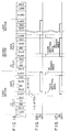
- a track has a format shown in Fig. 1A, i.e. in which one sector comprises an ID field and a data field.
- the ID field comprises a synchronization area SYNC, an address mark area AM, an identification area ID, and a cyclic redundancy check area CRC. Information representative of the starting position and address of a sector are recorded in the ID field.
- the data field stores data, and comprises synchronization area SYNC, address mark area AM, data area DATA, and cyclic redundancy check area CRC.
- Synchronization areas SYNC of the ID field and the data field store synchronization data for a PLL circuit; address mark areas AM store address mark data indicative of the starting position of the ID field or the data field; ID area ID stores data such as the cylinder number, the side number, the sector number, and the length of the data field; data area DATA stores data read out or written in by a user; and cyclic redundancy check areas CRC store data for checking whether or not the data read out from the ID field or from data field contains an error.
- Gaps 1, 2, 3, and 4 are areas for absorbing a fluctuation of rotation and an error in a mechanical alignment.
- Read data reproduced from the recording medium by the magnetic head are supplied to a data separator which includes a PLL circuit and an external synchronization detecting circuit.
- the external synchronization detector detects the synchronization data in the read data, and upon detection of the synchronization data, the PLL circuit begins oscillating in synchronism with the read data and outputs data pulses and clock pulses.
- an internal synchronization detector detects the synchronization data, on the basis of the data pulse and the clock pulse, and a floppy disk controller checks whether or not the following data, other than synchronization data, are address mark data.
- the floppy disk controller When the address mark data are detected, the floppy disk controller reads out the data stored in the ID area ID or in data area DATA, on the basis of the data pulses and clock pulses. When data other than the address mark data are detected, the floppy disk controller stops operating for a predetermined time period, and then repeats the above-mentioned operation.
- Figs. 1B and 1C show the positions where the erase head and read/write head of the preceding-erase type magnetic head are turned on and off, during data are written in the medium. As is shown in Figs. 1A to 1C, DC erased areas are formed in Gap 3, where data are erased by the erase head and new data are not recorded.
- Prior art document EP-A-0 139 757 describes an apparatus for reproducing a data signal from a recording medium on which a digital data signal, which is processed according to run length limited code modulation, is recorded with a synchronizing signal portion.
- the apparatus is arranged so that the supply of a rectangular-wave reproduction signal from a waveform shaping unit to a reproduction signal processing unit is inhibited when the amplitude of a read signal detected by an amplitude detection unit is lower than a predetermined value, thereby preventing erroneous detection of the synchronizing signal.
- the apparatus is suitable for the reproduction of a data signal from a digital audio disc and prevents an erroneous detection of the synchronizing signal when there is a defective part on the recording surface of the recording medium.
- Prior art document EP-A-0 146 636 discloses a synchronizing circuit in which data signals are divided into groups of a predetermined number of bits, each having a synchronizing signal, any desired address signal and an error detection signal for detecting an error of the address signal.
- the groups of data signals are adapted to be written in a memory device in accordance with the address signals.
- the synchronizing circuit has means for detecting any error in the address signal, means for detecting the synchronizing signal, an internal synchronizing signal generating circuit and an internal address signal generating circuit.
- the internal synchronizing signal generating circuit is driven, when the error detecting means judges that the address signal is correct so that an internal synchronizing signal drives the internal address signal generating circuit.
- the address signal or the internal address signal is selectively supplied to the memory device depending on whether the address signal is correct or wrong. In this way, data blocks syncs are suppressed if a following block address cannot be detected, i.e. if data is misinterpreted as a sync pattern.
- the present invention provides a magnetic recording/reproducing system as stated in claim 1.
- the digital signal (RD) which is reproduced from the DC erased areas in the tracks (such as GAP3) is not output.
- the data recorded in the magnetic recording medium (21) can be reliably read out.
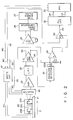
- FIG. 2 is a block diagram illustrating a first embodiment of this invention.
- magnetic head 20 is a magnetic head of the preceding-erase type, which has erase head 20A, read/write head 20B and separator 20C. Separator 20C magnetically separates erase head 20A from read/write head 20B. Erase head 20A is located in front of read/write head 20B with respect to the rotational direction of the medium 21.
- FDC 33 receives write data WD from a host computer (not shown), and supplies write data WD to write circuit 47.
- FDC 33 also supplies gate signal GS to write circuit 47 and selector 46.
- Gate signal GS functions as write gate signal WG, erase gate signal EG and select signal SS.
- Write gate signal WG and erase gate signal EG are supplied to write circuit 47.
- Select signal SS is supplied to selector 46.
- Selector 46 supplies write signal WS to read/write head 20B when select signal SS is H level.
- Selector 46 supplies output signal of read/write head 20B to preamplifier 22 when select signal SS is L level.
- the output signal of head 20 is supplied to preamplifier 22.
- Pre-amplifier 22 amplifies the output signal of magnetic head 20.
- the output signal of pre-amplifier 22 is supplied to AGC (automatic gain controlled) amplifier 24 via low-pass filter 23.
- Low-pass filter 23 removes the high-frequency noise of the output signal of pre-amplifier 22.
- AGC amplifier 24 keeps constant the amplitude of the output signal, and has a control terminal for gain adjustment.
- Output signal SA of AGC amplifier 24 is supplied to differential amplifier 25. Differential amplifier 25 detects peaks of output signal SA of AGC amplifier 24.
- the output signal of differential amplifier 25 is supplied to zero cross comparator 26.
- Zero cross comparator 26 outputs a pulse whose polarity is inverted at each zero cross point of output signal of differential amplifier 25, that is, each peak of the output signal SA of AGC amplifier 24.
- the output signal of zero cross comparator 26 is supplied to time domain filter 27.
- Time domain filter 27 removes pulses at abnormal intervals (erroneous pulses) caused by external noises and the like contained in the pulse signal from zero cross comparator 26. Filter 27 then outputs the pulse of normal intervals as the read data pulse.
- the output signal of time domain filter 27 is input to interface driver 30.
- Output signal SA of AGC amplifier 24 is also supplied to envelope detection circuit 28.
- Envelope detection circuit 28 detects signal SA to obtain the envelope of signal SA.
- Envelope detection circuit 28 outputs detect result SEN (a signal which corresponds to the detected envelope) to the terminal for gain adjustment of AGC amplifier 24. According to the signal level of signal SEN, the gain of AGC circuit 24 is controlled, so that an output signal of a constant amplitude is obtained.
- the output signal SEN of envelope detection circuit 28 is also supplied to the inverting input terminal of comparator 29.
- the reference voltage Vr is supplied to the non-inverting input terminal of comparator 29.
- Comparator 29 supplies signal E to the control terminal of interface driver 30.
- Signal E is high in level when the output voltage of envelope detection circuit 28 is below the reference voltage Vr.
- interface driver 30 When signal E from comparator 29 is low, interface driver 30 is in an operable state, and supplies the output signal of time domain filter 27 to magnetic record/reproduction system 31 as read data RD.
- PLL circuit 32 internally includes a voltage controlled oscillator (not shown). PLL circuit 32 operates so that the phase of the output pulses are equal to that of the input pulses. PLL circuit 32 oscillates in synchronism with read data RD. It then separates read data RD into data pulses DP and clock pulses CP. Data pulses DP is a pulse signal which represents the data recorded on the tracks of magnetic recording medium 21. Clock pulses CP is a pulse signal which represents the timing for reading the data.
- FDC 33 is connected to a host computer (not shown), for example. In response to the command of the host computer, FDD 30 performs the data read-out on the basis of data pulses DP and clock pulses CP.
- the host computer supplies a write command to FDC 33.
- FDC 33 causes gate signal GS to rise to H level.
- Gate signal GS functions as write gate signal WG, erase gate signal EG and select signal SS.
- Write circuit 47 receives signals WG and EG. When write gate signal WG and erase signal EG rise to H level, write circuit 47 generates write signal WS and erase signal ES on the bases of write data WD supplied from hose computer via FDC 33 to write circuit 47.
- Write circuit 47 supplies write signal WS to selector 46, and erase signal ES to erase head 20B.
- select signal SS rises to H level, selector 46 supplied write signal WS, which has been supplied from write circuit, to read/write head 20A.
- the data recorded on medium 21 is erased by erase head 20B, and new data is recorded on medium 21 by the read/write head 20A.
- FDC 33 causes gate signal GS fall to L level.
- gate signal GS falls to L level
- write circuit 47 stops generating erase signal ES and write signal WS.
- write signal WS is not supplied to read/write head 20A
- read/write head 20A reads the data recorded on medium 21, and outputs a signal corresponding to this data.
- selector 46 supplies the output signal of read/write head 20A to preamplifier 22.
- Each track of magnetic recording medium 21 also has a format shown in Fig. 1A.
- the on/off timings of the erase head and the read/write head when the data is recorded, are same as Figs. 1B and 1C.
- the output signal of magnetic head 20 is supplied to AGC amplifier 24 via pre-amplifier 22 and low-pass filter 23.
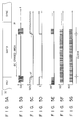
- AGC amplifier 24 outputs signal SA of a constant amplitude, as shown in Fig. 3B.
- the output signal of AGC amplifier 24 is differentiated by differential amplifier 25.
- the differential signal is input to zero cross comparator 26.
- Differential output signal SA of AGC amplifier 24 is converted into a pulse signal by zero cross comparator 26.
- the pulse signal is input to interface driver 30 as read data pulse signal, after its abnormal pulses are removed by time domain filter 27.
- Envelope detection circuit 28 detects the envelope of output signal SA of AGC amplifier 24, and output signal SEN (which corresponds to the envelope), as shown in Fig. 3C. On the basis of the signal level of signal SEN, the amplification of AGC amplifier 24 changes, so that output signal SA of a consant amplitude is obtained.
- Comparator 29 receives signal SEN, and outputs low-level signal E, because the voltage level of signal SEN is larger than the reference voltage Vr (Fig. 3D). Vr is set to such a level that, in the normal state, the voltage level of signal SEN is larger than the reference voltage.
- interface driver 30 supplies the read data pulse from time domain filter 27 to magnetic record/reproduction system 31.
- the PLL circuit 32 of magnetic record/reproduction system 31 oscillates in synchronism with read data RD, and separates read data RD into data pulse DP and clock pulse CP.
- FDC 33 performs the data read-out.
- the amplitude of the output signal of pre-amplifier 22 is substantially zero.
- the amplitude of output signal SA of AGC amplifier 24 is also substantially zero, as shown in Fig. 3B.
- the output of time domain filter 27 is instable.
- Signal SEN is at zero level, which is below the reference voltage level Vr, as shown in Fig. 3C.
- Comparator 29 outputs high-level signal E.
- interface driver 30 Upon receipt of low-level signal E, interface driver 30 is in a high output impedance state, and does not input read data RD.
- PLL circuit 32 oscillates, while keeping the oscillating frequency up to this point.
- AGC amplifier 24 When magnetic head 20 moves out of the DC erased area, and reads the data recorded area (SYNC), again, AGC amplifier 24 outputs signal SA of a predetermined amplitude, as shown in Fig. 3B. Signal SEN exceeds the reference voltage level Vr, and the output signal of comparator 29 becomes low in level. Interface driver 30 transfers the read data pulse from time domain filter 27 to record/reproduction circuit 31 (Fig. 3E).
- read data RD is not output from interface driver 30.
- Fig. 4 FDP The structural features of the Fig. 4 FDP, as compared with the Fig. 2 FDP, are: (1) Selector 41 is provided instead of interface driver 30; (2) Oscillator 42 and frequency divider 43 are additionally used; (3) Buffer 44 is additionally used; and (4) The polarities of the input terminal of comparator 29 are opposite to those of the comparator 29 in the first embodiment.
- Selector 41 receives the output of time domain filter 27 at input terminal A, and the output signal of frequency divider 43, at input terminal B.
- Selector 41 receives the output signal E of comparator 29 at the select control terminal SEL.
- separator 29 selects read data pulse RP from time domain filter 27, and outputs the pulse RP to buffer 44.
- selector 41 selects the clock signal from frequency divider 43, and outputs the clock signal to buffer 44.
- a system clock generating circuit used in the controller of a floppy disk apparatus may be used, for example.
- Frequency divider 44 frequency divides the clock signal from oscillator 42, and outputs a clock at a frequency corresponding to the transfer rate of the normal read data RD.
- Figs. 5A to 5G The operation of the second embodiment of Fig. 4 will be described, referring to Figs. 5A to 5G.
- AGC amplifier 24 outputs signal SA of a predetermined amplitude (Fig. 5B).
- Signal SEN is in level above the reference level Vr (Fig. 5C), and output signal E of comparator 29 is high in level.
- selector 41 selects the output signal RP of time domain filter 27 (Fig. 5E) and outputs signal RD.
- Output data RD of selector 41 is supplied to magnetic record/reproduction system 31 via buffer 44.
- the clock SD from frequency divider 43 is a pulse signal at a frequency corresponding to the transfer rate of the normal read data RD.
- PLL circuit 32 (not shown in Fig. 4) in the data separator oscillates in synchronism with the input data, in the same manner as when normal read data RD is supplied.
- the read data reproduced from the DC erased areas of the magnetic recording medium is prevented from being supplied to the magnetic record/reproduction system.
- the read data with a high reliability can be obtained.
- Circuit configuration of this invention is not limited to those of Figs. 2 and 4. Other circuit configuration can be selected.
- FDC 33 may be provided in a magnetic disk apparatus or outside of the apparatus.
Landscapes
- Engineering & Computer Science (AREA)
- Signal Processing (AREA)
- Physics & Mathematics (AREA)
- General Physics & Mathematics (AREA)
- Theoretical Computer Science (AREA)
- Digital Magnetic Recording (AREA)
- Signal Processing For Digital Recording And Reproducing (AREA)
Claims (10)
- Magnetaufzeichnungs/Wiedergabesystem für Magnetplattengerät, mit:
einer Kopfeinrichtung (20, 22-24) mit einem Voreillöschtyp-Magnetkopf (20) in Berührung mit einem flexiblen magnetischen Aufzeichnungsmedium (21) zum Auslesen von in dem Aufzeichnunungsmedium (21) gespeicherten Daten und zum Ausgeben eines Analogsignales entsprechend den ausgelesenen Daten und einer Umsetzereinrichtung (25-27) zum Umsetzen des Ausgangssignales der Kopfeinrichtung (20, 22-24) in digitale Lesedaten und zum Ausgeben der digitalen Lesedaten, gekennzeichnet durch eine Verhinderungseinrichtung (28-30), die die Umsetzereinrichtung (25-27) daran hindert, die digitalen Lesedaten auszugeben, die Auslesedaten von gleichstromgelöschten Bereichen in Spuren des magnetischen Aufzeichnungsmediums (21) entsprechen. - System nach Anspruch 1, bei dem die Verhinderungseinrichtung (28-30) eine Amplitudendetektoreinrichtung (28) zum Detektieren der Amplitude des Ausgangssignales von der Kopfeinrichtung (20), eine Einrichtung (29) zum Vergleichen der durch die Amplitudendetektoreinrichtung (28) detektierten Amplitude mit einem vorbestimmten Bezugspegel und eine Einrichtung (30), die verhindert, daß das Signal der Umsetzereinrichtung (25-27) ausgegeben wird, wenn die Amplitude niedriger ist als der vorbestimmte Bezugspegel, aufweist.
- System nach Anspruch 2, bei dem die Magnetkopfeinrichtung (20, 22-24) einen automatischen Verstärkungsfaktor-Steuerverstärker (24) zum Verstärken des Ausgangssignales des Magnetkopfes (20) aufweist, bei dem die Amplitudendetektoreinrichtung (28) eine Einrichtung zum Gewinnen der Umhüllung des Ausgangssignales des Verstärkungsfaktor-Steuerverstärkers (24) aufweist und bei dem die Vergleichereinrichtung (29) eine Einrichtung zum Vergleichen der Umhüllung mit dem Bezugssignal aufweist.
- System nach Anspruch 1, bei dem die Verhinderungseinrichtung (28-30) eine Einrichtung (28) zum Detektieren einer Umhüllung des Ausgangssignales der Kopfeinrichtung (20, 22-24), eine Einrichtung (29) zum Vergleichen der durch die Umhüllungsdetektoreinrichtung (28) detektierten Umhüllung mit einem vorbestimmten Bezugspegel und eine Einrichtung (30), die verhindert, daß das Signal der Umsetzereinrichtung (25-30) ausgegeben wird, wenn der Signalpegel der detektierten Umhüllung niedriger ist als der vorbestimmte Bezugspegel, aufweist.
- System nach Anspruch 1, gekennzeichnet durch eine Einrichtung (42, 43) zum Ausgeben eines Taktsignales mit einer vorbestimmten Frequenz und bei der die Verhinderungseinrichtung (28, 29, 41) das Taktsignal auswählt und ausgibt, wenn die Verhinderungseinrichtung (28, 29, 41) die Ausgabe der Lesedaten verhindert.
- System nach Anspruch 1, bei dem die Umsetzereinrichtung (25-27) die digitalen Lesedaten zu einer PLL-Schaltung (32) eines Datentrenners speist.
- System nach Anspruch 1, bei dem die Verhinderungseinrichtung (28-30) eine Detektoreinrichtung (28, 29) für einen gleichstromgelöschten Bereich zum Detektieren eines von den gleichstromgelöschten Bereichen wiedergegebenen Signales aufweist und bei dem die Verhinderungseinrichtung (30) die Umsetzereinrichtung (25-27) daran hindert, die digitalen Lesedaten abhängig von einer derartigen Detektion durch die Detektoreinrichtung (28, 29) für den gleichstromgelöschten Bereich auszugeben.
- System nach Anspruch 1, bei dem die Kopfeinrichtung eine Analogsignal-Ausgabeeinrichtung (22, 23, 24) zum Ausgeben eines Lesesignales eines analogen Typs entsprechend aufgezeichneten Daten aufweist, die durch den Magnetkopf (20) von dem magnetischen Aufzeichnungsmedium (21) ausgelesen sind.
- System nach Anspruch 1, bei dem die Verhinderungseinrichtung (28-30) eine Amplitudendetektoreinrichtung (28) zum Detektieren der Amplitude des Ausgangssignales von der Kopfeinrichtung (20), eine Einrichtung (29) zum Vergleichen der durch die Amplitudendetektoreinrichtung (28) detektierten Amplitude mit einem vorbestimmten Bezugswert und eine Einrichtung (30), die die Umsetzereinrichtung (25-27) daran hindert, die digitalen Lesedaten zu einer PLL-Schaltung (32) auszugeben, wenn die Amplitude kleiner als der vorbestimmte Bezugswert ist, aufweist.
- System nach Anspruch 1, bei dem die Verhinderungseinrichtung (30) eine Umhüllungsdetektoreinrichtung (28) zum Erzeugen eines Umhüllungssignales des Signales von der Magnetkopfeinrichtung (20, 22-24), eine Einrichtung (29) zum Vergleichen des Umhüllungssignales mit einem vorbestimmten Bezugswert und eine Einrichtung (30), die die Umsetzereinrichtung (25-27) daran hindert, die digitalen Lesedaten zu einer PLL-Schaltung auszugeben, wenn die Amplitude des Umhüllungssignales kleiner als der vorbestimmte Bezugswert ist, aufweist.
Applications Claiming Priority (2)
| Application Number | Priority Date | Filing Date | Title |
|---|---|---|---|
| JP61153531A JPS639005A (ja) | 1986-06-30 | 1986-06-30 | 磁気記録再生装置 |
| JP153531/86 | 1986-06-30 |
Publications (3)
| Publication Number | Publication Date |
|---|---|
| EP0251276A2 EP0251276A2 (de) | 1988-01-07 |
| EP0251276A3 EP0251276A3 (en) | 1989-09-20 |
| EP0251276B1 true EP0251276B1 (de) | 1992-08-19 |
Family
ID=15564558
Family Applications (1)
| Application Number | Title | Priority Date | Filing Date |
|---|---|---|---|
| EP87109330A Expired - Lifetime EP0251276B1 (de) | 1986-06-30 | 1987-06-29 | System zur Aufzeichnung und Wiedergabe für magnetisches Aufzeichnungsmedium |
Country Status (5)
| Country | Link |
|---|---|
| US (1) | US4809090A (de) |
| EP (1) | EP0251276B1 (de) |
| JP (1) | JPS639005A (de) |
| KR (1) | KR910001395B1 (de) |
| DE (1) | DE3781213T2 (de) |
Families Citing this family (7)
| Publication number | Priority date | Publication date | Assignee | Title |
|---|---|---|---|---|
| JP2549153B2 (ja) * | 1988-08-11 | 1996-10-30 | 富士通株式会社 | データリード回路 |
| JP2852165B2 (ja) * | 1991-11-12 | 1999-01-27 | 三星電子株式会社 | ディジタル磁気記録再生装置のピックアップ信号補正装置 |
| KR0170261B1 (ko) * | 1992-09-02 | 1999-04-15 | 김광호 | 최적 기록/재생장치 |
| JPH06150216A (ja) * | 1992-11-02 | 1994-05-31 | Sony Corp | ディジタル信号再生方法とその装置 |
| US5392171A (en) * | 1993-01-07 | 1995-02-21 | Seagate Technology, Inc. | Fully integrated programmable filters for disc drive subsystems |
| US5412516A (en) * | 1993-02-25 | 1995-05-02 | Hewlett-Packard Company | Data storage system with a dual-gap head using a dual-mode flexible disk controller |
| KR100583631B1 (ko) * | 2005-09-23 | 2006-05-26 | 주식회사 아나패스 | 클록 신호가 임베딩된 멀티 레벨 시그널링을 사용하는디스플레이, 타이밍 제어부 및 컬럼 구동 집적회로 |
Citations (1)
| Publication number | Priority date | Publication date | Assignee | Title |
|---|---|---|---|---|
| JPH06139911A (ja) * | 1992-10-21 | 1994-05-20 | Mitsubishi Electric Corp | 回路遮断器 |
Family Cites Families (6)
| Publication number | Priority date | Publication date | Assignee | Title |
|---|---|---|---|---|
| JPS5339722A (en) * | 1976-09-24 | 1978-04-11 | Nec Corp | Synchronous circuit using artificial information |
| JPS53142386A (en) * | 1977-05-18 | 1978-12-12 | Toshiba Ceramics Co | Low carbon silicon single crystal manufacturing apparatus |
| JPS5731224A (en) * | 1980-08-02 | 1982-02-19 | Toshiba Corp | Magnetic recording and reproducing circuit |
| JPS5967731A (ja) * | 1982-10-12 | 1984-04-17 | Matsushita Electric Ind Co Ltd | 位相ロツクド・ル−プ回路 |
| US4553178A (en) * | 1983-01-18 | 1985-11-12 | Electronic Processors, Inc. | Magnetic recording system with peak shift compensation |
| JPS59165212A (ja) * | 1983-03-08 | 1984-09-18 | Sony Corp | 情報信号再生装置 |
-
1986
- 1986-06-30 JP JP61153531A patent/JPS639005A/ja active Pending
-
1987
- 1987-06-29 DE DE8787109330T patent/DE3781213T2/de not_active Expired - Fee Related
- 1987-06-29 EP EP87109330A patent/EP0251276B1/de not_active Expired - Lifetime
- 1987-06-29 KR KR1019870006617A patent/KR910001395B1/ko not_active Expired
-
1988
- 1988-07-20 US US07/222,376 patent/US4809090A/en not_active Expired - Fee Related
Patent Citations (1)
| Publication number | Priority date | Publication date | Assignee | Title |
|---|---|---|---|---|
| JPH06139911A (ja) * | 1992-10-21 | 1994-05-20 | Mitsubishi Electric Corp | 回路遮断器 |
Also Published As
| Publication number | Publication date |
|---|---|
| EP0251276A2 (de) | 1988-01-07 |
| JPS639005A (ja) | 1988-01-14 |
| KR880000882A (ko) | 1988-03-30 |
| EP0251276A3 (en) | 1989-09-20 |
| US4809090A (en) | 1989-02-28 |
| KR910001395B1 (ko) | 1991-03-04 |
| DE3781213T2 (de) | 1993-03-11 |
| DE3781213D1 (de) | 1992-09-24 |
Similar Documents
| Publication | Publication Date | Title |
|---|---|---|
| US5838512A (en) | Apparatus for reproducing digital servo data and digital user data, for use in a disk storage system | |
| EP0974966B1 (de) | Plattenaufzeichnungssystem | |
| US6178053B1 (en) | Storage apparatus for reducing a read error caused by a thermal asperity of a magneto-resistive head | |
| US5467331A (en) | Recording and reproducing apparatus having arrangement for recovery of read-out data error | |
| JPH07264057A (ja) | 位相同期回路および記録再生装置 | |
| US5801896A (en) | Method and apparatus for servo pulse detection with high AC coupling and large pulse asymmetry | |
| EP0251276B1 (de) | System zur Aufzeichnung und Wiedergabe für magnetisches Aufzeichnungsmedium | |
| US7184236B2 (en) | Magnetic hard disk drive | |
| US5982308A (en) | Technique for compensation for missing pulses when decoding gray code data in hard disk drive | |
| US4897740A (en) | Recording/reproducing system for a magnetic recording medium including synchronization detecting circuit | |
| US4811126A (en) | Recording/reproducing system for a magnetic recording medium including synchronization detecting circuit | |
| US20020023248A1 (en) | Medium defect detection method and data storage apparatus | |
| US6229660B1 (en) | Method and apparatus for reading information recording field of hard disk drive to enable reliable adjustment of automatic gain control and phase-locked loop | |
| US6208476B1 (en) | Data recording device and method for recording data on a magnetic tape with error correction | |
| US5644446A (en) | Rotary-head digital reproducing/recording method and apparatus with block address-based area signal generation | |
| US6307693B1 (en) | Integration of filter into read/write preamplifier integrated circuit | |
| JP2948445B2 (ja) | 回転ヘッド式デジタルデータ記録/再生方法及び装置 | |
| KR950004268Y1 (ko) | 디스크 구동장치의 데이터 검출레벨 조정회로 | |
| JP2549211Y2 (ja) | 磁気記録再生装置における記録エラー検出装置 | |
| JP2815283B2 (ja) | データ再生装置 | |
| JPH04295673A (ja) | ドロップアウト検出回路 | |
| JPH0991875A (ja) | 磁気ディスク装置の信号読み出し回路 | |
| JPH02208874A (ja) | 読出しエラーに対する再試行方式 | |
| JPH0589607A (ja) | データ再生装置 | |
| JPH04295674A (ja) | 磁気記録媒体の検査装置 |
Legal Events
| Date | Code | Title | Description |
|---|---|---|---|
| PUAI | Public reference made under article 153(3) epc to a published international application that has entered the european phase |
Free format text: ORIGINAL CODE: 0009012 |
|
| 17P | Request for examination filed |
Effective date: 19870724 |
|
| AK | Designated contracting states |
Kind code of ref document: A2 Designated state(s): DE FR GB IT |
|
| PUAL | Search report despatched |
Free format text: ORIGINAL CODE: 0009013 |
|
| AK | Designated contracting states |
Kind code of ref document: A3 Designated state(s): DE FR GB IT |
|
| 17Q | First examination report despatched |
Effective date: 19910207 |
|
| GRAA | (expected) grant |
Free format text: ORIGINAL CODE: 0009210 |
|
| AK | Designated contracting states |
Kind code of ref document: B1 Designated state(s): DE FR GB IT |
|
| ITF | It: translation for a ep patent filed | ||
| REF | Corresponds to: |
Ref document number: 3781213 Country of ref document: DE Date of ref document: 19920924 |
|
| ET | Fr: translation filed | ||
| PLBE | No opposition filed within time limit |
Free format text: ORIGINAL CODE: 0009261 |
|
| STAA | Information on the status of an ep patent application or granted ep patent |
Free format text: STATUS: NO OPPOSITION FILED WITHIN TIME LIMIT |
|
| 26N | No opposition filed | ||
| PGFP | Annual fee paid to national office [announced via postgrant information from national office to epo] |
Ref country code: FR Payment date: 19980609 Year of fee payment: 12 |
|
| PGFP | Annual fee paid to national office [announced via postgrant information from national office to epo] |
Ref country code: GB Payment date: 19980622 Year of fee payment: 12 |
|
| PGFP | Annual fee paid to national office [announced via postgrant information from national office to epo] |
Ref country code: DE Payment date: 19980706 Year of fee payment: 12 |
|
| PG25 | Lapsed in a contracting state [announced via postgrant information from national office to epo] |
Ref country code: GB Free format text: LAPSE BECAUSE OF NON-PAYMENT OF DUE FEES Effective date: 19990629 |
|
| PG25 | Lapsed in a contracting state [announced via postgrant information from national office to epo] |
Ref country code: FR Free format text: THE PATENT HAS BEEN ANNULLED BY A DECISION OF A NATIONAL AUTHORITY Effective date: 19990630 |
|
| GBPC | Gb: european patent ceased through non-payment of renewal fee |
Effective date: 19990629 |
|
| PG25 | Lapsed in a contracting state [announced via postgrant information from national office to epo] |
Ref country code: DE Free format text: LAPSE BECAUSE OF NON-PAYMENT OF DUE FEES Effective date: 20000503 |
|
| REG | Reference to a national code |
Ref country code: FR Ref legal event code: ST |
|
| PG25 | Lapsed in a contracting state [announced via postgrant information from national office to epo] |
Ref country code: IT Free format text: LAPSE BECAUSE OF NON-PAYMENT OF DUE FEES;WARNING: LAPSES OF ITALIAN PATENTS WITH EFFECTIVE DATE BEFORE 2007 MAY HAVE OCCURRED AT ANY TIME BEFORE 2007. THE CORRECT EFFECTIVE DATE MAY BE DIFFERENT FROM THE ONE RECORDED. Effective date: 20050629 |