EP0251828A1 - Isolierharz-Zusammensetzung und Halbleitervorrichtung unter deren Verwendung - Google Patents
Isolierharz-Zusammensetzung und Halbleitervorrichtung unter deren Verwendung Download PDFInfo
- Publication number
- EP0251828A1 EP0251828A1 EP87305975A EP87305975A EP0251828A1 EP 0251828 A1 EP0251828 A1 EP 0251828A1 EP 87305975 A EP87305975 A EP 87305975A EP 87305975 A EP87305975 A EP 87305975A EP 0251828 A1 EP0251828 A1 EP 0251828A1
- Authority
- EP
- European Patent Office
- Prior art keywords
- acid dianhydride
- resin composition
- insulating resin
- group
- composition according
- Prior art date
- Legal status (The legal status is an assumption and is not a legal conclusion. Google has not performed a legal analysis and makes no representation as to the accuracy of the status listed.)
- Granted
Links
- 0 O=*1[O+]*C*1 Chemical compound O=*1[O+]*C*1 0.000 description 1
Images

Classifications
-
- H—ELECTRICITY
- H10—SEMICONDUCTOR DEVICES; ELECTRIC SOLID-STATE DEVICES NOT OTHERWISE PROVIDED FOR
- H10P—GENERIC PROCESSES OR APPARATUS FOR THE MANUFACTURE OR TREATMENT OF DEVICES COVERED BY CLASS H10
- H10P14/00—Formation of materials, e.g. in the shape of layers or pillars
- H10P14/60—Formation of materials, e.g. in the shape of layers or pillars of insulating materials
- H10P14/68—Organic materials, e.g. photoresists
- H10P14/683—Organic materials, e.g. photoresists carbon-based polymeric organic materials, e.g. polyimides, poly cyclobutene or PVC
-
- C—CHEMISTRY; METALLURGY
- C08—ORGANIC MACROMOLECULAR COMPOUNDS; THEIR PREPARATION OR CHEMICAL WORKING-UP; COMPOSITIONS BASED THEREON
- C08G—MACROMOLECULAR COMPOUNDS OBTAINED OTHERWISE THAN BY REACTIONS ONLY INVOLVING UNSATURATED CARBON-TO-CARBON BONDS
- C08G73/00—Macromolecular compounds obtained by reactions forming a linkage containing nitrogen with or without oxygen or carbon in the main chain of the macromolecule, not provided for in groups C08G12/00 - C08G71/00
- C08G73/06—Polycondensates having nitrogen-containing heterocyclic rings in the main chain of the macromolecule
- C08G73/10—Polyimides; Polyester-imides; Polyamide-imides; Polyamide acids or similar polyimide precursors
- C08G73/1057—Polyimides containing other atoms than carbon, hydrogen, nitrogen or oxygen in the main chain
- C08G73/106—Polyimides containing other atoms than carbon, hydrogen, nitrogen or oxygen in the main chain containing silicon
-
- H—ELECTRICITY
- H01—ELECTRIC ELEMENTS
- H01B—CABLES; CONDUCTORS; INSULATORS; SELECTION OF MATERIALS FOR THEIR CONDUCTIVE, INSULATING OR DIELECTRIC PROPERTIES
- H01B3/00—Insulators or insulating bodies characterised by the insulating materials; Selection of materials for their insulating or dielectric properties
- H01B3/18—Insulators or insulating bodies characterised by the insulating materials; Selection of materials for their insulating or dielectric properties mainly consisting of organic substances
- H01B3/30—Insulators or insulating bodies characterised by the insulating materials; Selection of materials for their insulating or dielectric properties mainly consisting of organic substances plastics; resins; waxes
-
- H—ELECTRICITY
- H10—SEMICONDUCTOR DEVICES; ELECTRIC SOLID-STATE DEVICES NOT OTHERWISE PROVIDED FOR
- H10W—GENERIC PACKAGES, INTERCONNECTIONS, CONNECTORS OR OTHER CONSTRUCTIONAL DETAILS OF DEVICES COVERED BY CLASS H10
- H10W20/00—Interconnections in chips, wafers or substrates
- H10W20/01—Manufacture or treatment
- H10W20/071—Manufacture or treatment of dielectric parts thereof
-
- H—ELECTRICITY
- H10—SEMICONDUCTOR DEVICES; ELECTRIC SOLID-STATE DEVICES NOT OTHERWISE PROVIDED FOR
- H10P—GENERIC PROCESSES OR APPARATUS FOR THE MANUFACTURE OR TREATMENT OF DEVICES COVERED BY CLASS H10
- H10P14/00—Formation of materials, e.g. in the shape of layers or pillars
- H10P14/60—Formation of materials, e.g. in the shape of layers or pillars of insulating materials
- H10P14/63—Formation of materials, e.g. in the shape of layers or pillars of insulating materials characterised by the formation processes
- H10P14/6326—Deposition processes
- H10P14/6342—Liquid deposition, e.g. spin-coating, sol-gel techniques or spray coating
Definitions
- This invention relates to an insulating resin composition and semiconductor device using the same, and more particularly it relates to a semiconductor device having a multi-level interconnection suitable for high integration.
- a first level interconnection layer is at first formed on the base of the semiconductor, followed by forming an insulating film thereon, then forming a through-hole at a predetermined part of the insulating film according to a known hot etching process to expose a portion of the first level interconnection layer, then forming a metal film which is to constitute a second level interconnection layer according to vacuum deposition or spattering method and further subjecting this film to hot etching to form the second level interconnection layer.
- a metal film composed mainly of aluminum has most often been used as the interconnection layers, and an inorganic insulating film composed mainly of SiO2 film or an organic resin insulating film of polyimide group resins has been used as the insulating film material.
- the interconnection layer is composed mainly of aluminum, it is necessary for preventing fusion of aluminum and running-through of fused aluminum into the joint of the semiconductor to restrict the temperature at which the insulating film is formed on the interconnection layer to 450°C or lower.
- the inorganic insulating film such as those of SiO2, silicon carbide, etc. should be formed at a relatively low temperature such as about 400°C according to chemical gas phase growth method, high frequency spattering method or the like.
- chemical gas phase growth method SiO2 film formed is liable to cause cracks. So that a film having a thickness of at most only 1 ⁇ m or less can be formed. Further according to the spattering method, the resulting inorganic insulating film has a low formation rate.
- the inorganic insulating film have had the following drawbacks. Since the film is formed faithfully reproducing the projections and depressions (step differences) of the lower interconnection layer as it is, it has an inferior step-covering ability and the upper interconnection layer is liable to cause disconnection on the lateral side of the step so that it is deficient in reliability.
- an organic resin film of polyimide group resin including polyimide having fluidity and a superior step-covering ability is formed as an insulating film on a interconnection layer to planarize the projections and depressions on the lower interconnection layer and thereby dissolve the problem of the step difference.
- polyimide a cured product of a polyamic acid polymer obtained by reacting an aromatic diamine with an aromatic tetracarboxylic acid dianhydride
- polyimide group resin e.g.
- a cured product of a polyamic acid polymer obtained by reacting an aromatic diamine, an aromatic tetracarboxylic acid dianhydride and an aromatic diaminocarbonic amide), for example, PIQ varnish (trademark of a product manufactured by Hitachi Chemical Company, Ltd.), etc. are used.
- This PIQ varnish is rotationapplied onto a lower interconnection layer, followed by volatizing the solvent component and then heating the resulting material to 200° to 400°C to form a cured film of PIQ.
- This vanish have been usually adjusted to a resin content of 10 to 20% by weight and a viscosity of 5 to 50 poises.
- ta thickness of an interconnection layer 3 formed on a semiconductor base 1
- tb thickness of a step-covering part remained after formation of an organic resin insulating film 4
- (1 - will be defined as a step-covering performance or a planarizing capability.
- the planarizing capability in the case where the polyimide or polyimide group resin is used is in the range of 0.15 to 0.4.
- the film thickness on the step-covering part is smaller than that of the plane part, so that when the etching on the plane part has reached a proper state, overetching occurs on the step-covering part.
- the etching accuracy becomes inferior and hence when the polyimide or polyimide group resin is used as the insulating film material, a through-hole of 5 ⁇ m square has been a practical limit.
- the object of the present invention is to provide an insulating resin composition and a semiconductor device using the same having overcome the above-mentioned drawbacks of the prior art, and having a superior step-covering capability to the interconnection layer and a superior fine etching performance in dry etching process.
- the present inventors have found that when a cured product of a polyamic acid ester oligomer is used as an insulating film material for a semiconductor device having multilevel interconnecting structure, the step-covering part of the lower interconnection layer is planarized, whereby there is no fear of disconnection drawback on the side surface of the step between the upper interconnection layer and the lower interconnection layer, and etching for the through-hole of fine insulating film becomes possible; thus it is possible to obtain a semiconductor device having multilevel interconnecting structure with a fine interconnection and a fine through-hole, suitable to high integration and having a high reliability.
- the present invention is directed to an insulating resin composition for semiconductor devices comprising a cured product of a polyamic acid ester oligomer obtained by reacting at least one member selected from the group consisting of aromatic diamines and diamino siloxanes with an aromatic tetracarboxylic acid ester obtained by reacting an aromatic tetracarboxylic acid dianhydride with at least one member selected from the group consisting of alcohols and alcohol derivatives.
- the polyamic acid ester oligomer used as an insulating film material on a interconnection layer in the present invention is obtained by reacting an aromatic tetracarboxylic acid ester obtained by reacting an aromatic tetracarboxylic acid dianhydride with at least one member selected from alcohols and alcohol derivatives if necessary in the presence of a solvent, with at least one member selected from aromatic diamines and diaminosiloxanes preferably in a nearly equimolar amount to the aromatic tetracarboxylic acid ester.
- ether-glycol solvents such as butyl-cellosolve, N-methyl-2-pyrrolidone, N,N-diethylformamide, dimethyl sulfoxide, etc. They are used alone or in an admixture of two kinds or more thereof.
- the aromatic tetracarboxylic acid dianhydride is expressed by the formula: wherein R1 represents a tetravalent aromatic hydrocarbon radical.
- R1 represents a tetravalent aromatic hydrocarbon radical.
- R1 represents a tetravalent aromatic hydrocarbon radical.
- examples thereof are 3,3',4,4'-benzophenonetetracarboxylic acid dianhydride, pyromellitic acid dianhydride, 3,3',4,4'-diphenyltetracarboxylic acid dianhydride, 1,2,5,6-naphthalenetetracarboxylic acid dianhydride, 2,3,6,7-naphthalenetetracarboxylic acid dianhydride, 2,3,5,6-pyridinetetracarboxylic acid dianhydride, 1,4,5,8-naphthalenetetracarboxylic acid dianhydride, 3,4,9,10-perylenetetracarboxylic acid dianhydride, 4,4'-s
- Examples of the alcohols or alcohol derivatives for esterifying the aromatic tetracarboxylic acid dianhydride are monohydric alcohols such as methanol, ethanol, propanol, isopropyl alcohol, butanol, etc., polyols such as ethylene glycol, propylene glycol, glycerine, trimethylpropane, etc., and as the alcohol derivatives, cellosolves, carbitols, etc.
- the aromatic diamines used in the present invention are expressed by the formula: H2N - R2 - NH2 wherein R2 represents a divalent aromatic hydrocarbon radical.
- R2 represents a divalent aromatic hydrocarbon radical.
- examples thereof are 4,4'-diaminodiphenyl ether, 4,4'-diaminodiphenylmethane, 4,4'-diaminodiphenyl sulfone, 4,4'-diaminodiphenyl sulfide, benzidine, metaphenylenediamine, paraphenylenediamine, 1,5-naphthalenediamine, 2,6-naphthalenediamine, etc. These are used alone or in an admixture of two kinds or more thereof.
- the diaminosiloxanes used in the present invention are expressed by the formula: wherein R3 represents a divalent hydrocarbon radical of 1 to 10 carbon atoms; R4, R5, R6 and R7 each represent a monovalent hydrocarbon radical of 1 to 10 carbon atoms and may be the same or different kinds; and n represents an integer of 1 to 10.
- R3 represents a divalent hydrocarbon radical of 1 to 10 carbon atoms
- R4, R5, R6 and R7 each represent a monovalent hydrocarbon radical of 1 to 10 carbon atoms and may be the same or different kinds
- n represents an integer of 1 to 10.
- compounds expressed by the following formulas are preferably used, and these are used alone or in an admixture of two kinds or more thereof:
- the aromatic diamines and diaminosiloxanes may be used in combination.
- Esterification of the aromatic tetracarboxylic acid dianhydrides in the present invention is carried out using an alcohol and/or an alcohol derivative in an equimolar amount or more relative to the aromatic tetracarboxylic acid dianhydrides.
- the reaction temperature varies depending on the solvent, alcohols and alcohol derivatives used and has no particular limitation, but for example when 3,3',4,4'-benzophenonetetracarboxylic acid dianhydride is reacted with ethanol in N-methyl-2-pyrrolidone for esterification, temperatures of 80° to 150°C are preferred. Further, in order to adjust the concentration after the esterification, an excess alcohol or alcohol derivative can be removed, but in this case, it is preferred to heat the alcohol or alcohol derivative to its boiling point or higher.
- the reaction of the aromatic tetracarboxylic acid ester with the aromatic diamine and/or the diaminosiloxane in order to make the heat resistance of the resulting cured product highest, it is preferred to react the aromatic tetracarboxylic acid with the aromatic diamine and/or the aminosiloxane in nearly equimolar amounts.
- reaction temperature is too high, the resulting polyamic acid ester oligomer is converted into an imide so that its solubility lowers and it is deposited; hence it is preferred to carry out the reaction at a reaction temperature up to 90°C at the highest.
- the concentration of the resin content in the polyamic acid ester oligomer can be varied within a range of 40 to 60% by weight and also the viscosity thereof can be varied within a range of 0.5 to 50 poises, it is possible to determine a proper content of resin and a viscosity in accordance with the thickness of the lower interconnection layer.
- the molecular weight of the oligomer is in the range of 500 to 20000, preferably 1000 to 10000.
- the above polyamic acid ester oligomer is applied onto a interconnection layer with a spinner or the like, followed by drying the resulting material at a temperature of 100° to 200°C, preferably 120° to 180°C, for preferably 1 to 2 hours and then curing the resulting material at a temperature of 300° to 400°C, preferably 320° to 380°C for preferably 1 to 2 hours, whereby an organic resin insulating film is formed.
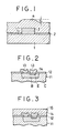
- Figs. 2-6 show schematic cross-sectional views illustrating steps for producing a semiconductor device of the present invention, where on a first interconnection layer 14 are formed an insulating film 15 and a second interconnection layer 18.
- a silicon dioxide film 12 is first formed on the surface of a semiconductor base 11 consisting of a collector region C, a base region B and an emitter region E according to a chemical gas-phase growth method.
- a definite portion which will constitute a portion connecting a lead terminal is removed by a photoetching method and a through-hole (window) 13 is provided in the silicon dioxide film 12 to expose the respective portions of the emitter region E and the base region B.
- an aluminum layer is formed on the through-hole 13 according to vacuum deposition or spattering method, and a first interconnection layer 14 is formed by a photoetching method.
- This interconnection layer had a thickness of 1 ⁇ m and a width of 2 to 5 ⁇ m.
- the polyamic acid ester oligomer used above was prepared by adding, 3,3',4,4'-benzophenonetetracarboxylic acid dianhydride (161.1g) and pyromellitic acid dianhydride (109.1g) to N,N-diethylformamide (700g), heating the mixture up to 80°C to dissolve it, adding ethanol (80g), reacting the mixture at 120°C for 3 hours, removing excess alcohol, cooling the resulting solution down to 80°C, adding to the solution.
- the thus prepared oligomer solution was applied for 30 seconds by means of a spinner so as to give a thickness of 3,000 ⁇ m and then subjected to heat curing treatment at 100°C for one hour, further at 200°C for one hour and still further at 350°C for one hour to form a film of a cured product of the above oligomer 15, as shown in Fig. 3.
- the thickness of the resulting resin film was 2.0 ⁇ m at the plane part on the silicon dioxide film 12 without the interconnection layer 14, the thickness of the resin film formed on the interconnection layer 14 was 1 ⁇ m and the planarizing capability was in the range of 0.85 to 0.90.
- chrome was vacuum-deposited on the film of the cured product 15 to prepare a chrome-vacuum-deposited film 16, followed by removing a predetermined portion of the chrome-vacuum-deposited film 16 i.e. a portion at which it was to be electrically connected with the first interconnection layer 14 according to photoetching method by the use of a novolak photosensitive resin to form an etching mask for forming a through-hole of 2 to 5 ⁇ m square, further removing the chrome-vacuum-deposited film 16 by means of oxygen gas under conditions of a pressure of 5 mm Torr, a power of 100W and an oxygen gas flow amount of 10 SCCM by the use of a reactive ion etching apparatus (CSE 2120, tradename of apparatus manufactured by Japan vacuum Technique Co., Ltd.), removing the exposed film of the cured product 15 by selective anisotropical etching to form a through-hole (window) 17 where the predetermined portion of the first interconnection layer 14 was exposed, and
- CSE 2120 reactive
- the thus obtained through-hole (window) 17 of the cured product film 15 had a tapered angle of 65 to 70° and also had through-hole dimensions of 2 ⁇ m square at the etching mask part of 2 ⁇ m square and 5 ⁇ m; thus the through-hole was formed with a very good accuracy, just in accordance with the designed dimensions of the etching mask, without depending on the dimensions of the throughhole.
- the film of the cured product obtained from the polyamic acid ester oligomer had a far superior planarizing capability and as shown in Fig. 6, when a through-hole is formed in the resin film 15 for electrically connecting the first interconnection layer 14 with the second interconnection layer 18, it is possible to form the chrome-vacuum-deposited film 16 for the etching mask very uniformly and planarly.
- a photoresist of novolak resin or the like is formed on the chrome-vacuum-deposited film uniformly and planarly and exposure is carried out uniformly; hence it is possible to form a fine pattern in a state of making use of the resolution of the photoresist so that it is possible to form a through-hole etching mask of fine 2 ⁇ m square of the resin film with a good accuracy. Still further, when a photoresist having a high resolution is used, it is possible to carry out through-hole etching of 2 ⁇ m or less.
- a second interconnection layer 18 is formed according to aluminum-vacuum deposition or spattering and photoetching, followed by forming a film of a cured product on the second interconnection layer 18 using a polyamic acid ester oligomer and then forming a through-hole on the resin film by through-hole etching method.
- a semiconductor device of a multilevel interconnecting structure according to the present invention is obtained. And by selecting the content of the resin, the viscosity and the thicknesses of the interconnection layers, it is possible to form resin films having a good planarizing capability.
- the semiconductor device of the present invention uses the above-mentioned polyamic acid ester oligomer as the insulating film material on the interconnection layer, and has a multilevel interconnecting structure having a superior step coating (planarizing capability) relative to the interconnection layer and also a superior fine through-hole etching capability according to dry etching method, having fine interconnection, and fine through-holes, being suitable to high integrate ion and having a high reliability.
- the semiconductor device of the present invention is suitable as a semiconductor device for hybrid IC, monolithic IC, LSI, etc.
Landscapes
- Chemical & Material Sciences (AREA)
- Physics & Mathematics (AREA)
- Spectroscopy & Molecular Physics (AREA)
- Health & Medical Sciences (AREA)
- Chemical Kinetics & Catalysis (AREA)
- Medicinal Chemistry (AREA)
- Polymers & Plastics (AREA)
- Organic Chemistry (AREA)
- Macromolecular Compounds Obtained By Forming Nitrogen-Containing Linkages In General (AREA)
- Formation Of Insulating Films (AREA)
- Internal Circuitry In Semiconductor Integrated Circuit Devices (AREA)
- Bipolar Transistors (AREA)
Applications Claiming Priority (2)
| Application Number | Priority Date | Filing Date | Title |
|---|---|---|---|
| JP61158554A JPH0727966B2 (ja) | 1986-07-04 | 1986-07-04 | 半導体装置 |
| JP158554/86 | 1986-07-04 |
Publications (2)
| Publication Number | Publication Date |
|---|---|
| EP0251828A1 true EP0251828A1 (de) | 1988-01-07 |
| EP0251828B1 EP0251828B1 (de) | 1993-09-22 |
Family
ID=15674242
Family Applications (1)
| Application Number | Title | Priority Date | Filing Date |
|---|---|---|---|
| EP87305975A Expired - Lifetime EP0251828B1 (de) | 1986-07-04 | 1987-07-06 | Isolierharz-Zusammensetzung und Halbleitervorrichtung unter deren Verwendung |
Country Status (5)
| Country | Link |
|---|---|
| US (1) | US5132386A (de) |
| EP (1) | EP0251828B1 (de) |
| JP (1) | JPH0727966B2 (de) |
| KR (1) | KR900005120B1 (de) |
| DE (1) | DE3787500T2 (de) |
Cited By (9)
| Publication number | Priority date | Publication date | Assignee | Title |
|---|---|---|---|---|
| EP0230615A3 (de) * | 1986-01-31 | 1989-11-08 | International Business Machines Corporation | Polyimide mit Silizium, verwendet als Stop für das Sauerstoff-Ätzen und als zusammengesetzte dielektrische Beschichtungen |
| EP0349010A1 (de) * | 1988-06-30 | 1990-01-03 | Nippon Steel Chemical Co., Ltd. | Polyimid-Copolymere |
| EP0361462A3 (en) * | 1988-09-28 | 1990-07-18 | Hitachi, Ltd. | Process for producing metal/polyimide composite article |
| EP0361461A3 (en) * | 1988-09-30 | 1990-12-19 | Hitachi, Ltd. | Process for producing metal-polyimide composite article |
| EP0459809A1 (de) * | 1990-06-01 | 1991-12-04 | Ube Industries, Ltd. | Polyimidosiloxan-Harz, Zusammensetzung daraus und Methode zur Anwendung |
| EP0377080A3 (de) * | 1988-12-21 | 1991-12-18 | W.L. Gore & Associates GmbH | Elektrischer Leiter, der mit einem Polymer isoliert ist |
| US5104968A (en) * | 1989-08-08 | 1992-04-14 | Centre D'etude Des Materiaux Organiques Pour Technologies Avancees | Polyimide precursor composition and application therefrom |
| US5268193A (en) * | 1988-06-28 | 1993-12-07 | Amoco Corporation | Low dielectric constant, low moisture uptake polyimides and copolyimides for interlevel dielectrics and substrate coatings |
| CN1094124C (zh) * | 1996-08-02 | 2002-11-13 | 罗狄亚纤维与树脂中间体公司 | 内酰胺的纯化方法 |
Families Citing this family (7)
| Publication number | Priority date | Publication date | Assignee | Title |
|---|---|---|---|---|
| US5310862A (en) * | 1991-08-20 | 1994-05-10 | Toray Industries, Inc. | Photosensitive polyimide precursor compositions and process for preparing same |
| US6294799B1 (en) * | 1995-11-27 | 2001-09-25 | Semiconductor Energy Laboratory Co., Ltd. | Semiconductor device and method of fabricating same |
| US5940732A (en) * | 1995-11-27 | 1999-08-17 | Semiconductor Energy Laboratory Co., | Method of fabricating semiconductor device |
| US20030158532A1 (en) | 2002-02-20 | 2003-08-21 | Magee Luke R. | Disposable absorbent article designed to facilitate an easy intuitive change |
| US8716548B2 (en) | 2002-02-20 | 2014-05-06 | The Procter & Gamble Company | Disposable absorbent article designed to facilitate an easy change |
| JP2009111333A (ja) * | 2007-10-12 | 2009-05-21 | Panasonic Corp | 半導体装置 |
| JP2014159551A (ja) * | 2013-01-28 | 2014-09-04 | Jnc Corp | 熱硬化性組成物、硬化膜および電子部品 |
Citations (2)
| Publication number | Priority date | Publication date | Assignee | Title |
|---|---|---|---|---|
| EP0071749A2 (de) * | 1981-08-12 | 1983-02-16 | National Starch and Chemical Corporation | Polyimide und deren polyamische Zwischenprodukte |
| EP0209114A2 (de) * | 1985-07-16 | 1987-01-21 | Kanegafuchi Kagaku Kogyo Kabushiki Kaisha | Amphiphiler Polyimid-Vorläufer und Verfahren zu seiner Herstellung |
Family Cites Families (18)
| Publication number | Priority date | Publication date | Assignee | Title |
|---|---|---|---|---|
| US3338859A (en) * | 1966-06-30 | 1967-08-29 | Dow Corning | Silicone polyimides |
| US3492270A (en) * | 1969-01-21 | 1970-01-27 | Du Pont | Crosslinked polyamide-acid and polyimide polymers |
| US3740305A (en) * | 1971-10-01 | 1973-06-19 | Gen Electric | Composite materials bonded with siloxane containing polyimides |
| US4030948A (en) * | 1975-07-21 | 1977-06-21 | Abe Berger | Polyimide containing silicones as protective coating on semiconductor device |
| US4051163A (en) * | 1975-07-21 | 1977-09-27 | Abe Berger | Polyimide containing silicones |
| JPS53107285A (en) * | 1977-03-02 | 1978-09-19 | Hitachi Ltd | Production of wiring structural body |
| US4299750A (en) * | 1979-05-03 | 1981-11-10 | Gulf Oil Corporation | Novel partially acetylene end-capped polyimide oligomers |
| JPS56118421A (en) * | 1980-02-25 | 1981-09-17 | Nitto Electric Ind Co Ltd | Heat-shrinkable polyimide film and production thereof |
| US4332708A (en) * | 1980-02-27 | 1982-06-01 | General Electric Company | Polycarboxylic acid/ester-diamine aqueous coating composition |
| US4485140A (en) * | 1983-09-21 | 1984-11-27 | E. I. Du Pont De Nemours And Company | Melt-fusible polyimides |
| US4467000A (en) * | 1983-03-29 | 1984-08-21 | International Business Machines Corporation | Process for coating a substrate with polyimide |
| US4520075A (en) * | 1983-09-02 | 1985-05-28 | Nitto Electric Industrial Co., Ltd. | Siloxane-modified polyimide precursor and polyimide |
| US4535099A (en) * | 1984-04-03 | 1985-08-13 | Imi-Tech Corporation | Polyimide foam from mixture of silicon containing diamine and different aromatic diamine |
| US4524171A (en) * | 1984-08-20 | 1985-06-18 | Gulf Oil Corporation | Preparation of an aromatic polyimide acid by solution polymerization using propylene glycol methyl ether |
| US4535115A (en) * | 1984-08-20 | 1985-08-13 | Gulf Oil Corporation | Method of preparation of polyimide acids |
| US4562100A (en) * | 1984-09-14 | 1985-12-31 | E. I. Du Pont De Nemours And Company | Polyimide coating compositions from diesterified anhydride and aromatic diamine |
| US4689391A (en) * | 1984-12-21 | 1987-08-25 | General Electric Company | Process for making polyetherimides |
| JPH0768347B2 (ja) * | 1985-09-25 | 1995-07-26 | 株式会社日立製作所 | 有機ケイ素末端ポリイミド前駆体とポリイミドの製造方法 |
-
1986
- 1986-07-04 JP JP61158554A patent/JPH0727966B2/ja not_active Expired - Lifetime
-
1987
- 1987-07-04 KR KR1019870007149A patent/KR900005120B1/ko not_active Expired
- 1987-07-06 DE DE87305975T patent/DE3787500T2/de not_active Expired - Lifetime
- 1987-07-06 EP EP87305975A patent/EP0251828B1/de not_active Expired - Lifetime
-
1989
- 1989-05-02 US US07/348,151 patent/US5132386A/en not_active Expired - Lifetime
Patent Citations (2)
| Publication number | Priority date | Publication date | Assignee | Title |
|---|---|---|---|---|
| EP0071749A2 (de) * | 1981-08-12 | 1983-02-16 | National Starch and Chemical Corporation | Polyimide und deren polyamische Zwischenprodukte |
| EP0209114A2 (de) * | 1985-07-16 | 1987-01-21 | Kanegafuchi Kagaku Kogyo Kabushiki Kaisha | Amphiphiler Polyimid-Vorläufer und Verfahren zu seiner Herstellung |
Non-Patent Citations (1)
| Title |
|---|
| CHEMICAL ABSTRACTS, vol. 95, no. 22, November 30, 1981, Columbus, Ohio, USA MAKINO, DAISUKE; SUZUKI, HIROSHI; KINJO, NORIYUKI "The characterization of PIQR and its application to semiconductor devices" page 634, abstract-no. 196 129c & Symp. Proc.-Univ./ Gov./ Ind. Microelectron. Symp., 4th 1981 * |
Cited By (12)
| Publication number | Priority date | Publication date | Assignee | Title |
|---|---|---|---|---|
| EP0230615A3 (de) * | 1986-01-31 | 1989-11-08 | International Business Machines Corporation | Polyimide mit Silizium, verwendet als Stop für das Sauerstoff-Ätzen und als zusammengesetzte dielektrische Beschichtungen |
| US5268193A (en) * | 1988-06-28 | 1993-12-07 | Amoco Corporation | Low dielectric constant, low moisture uptake polyimides and copolyimides for interlevel dielectrics and substrate coatings |
| EP0349010A1 (de) * | 1988-06-30 | 1990-01-03 | Nippon Steel Chemical Co., Ltd. | Polyimid-Copolymere |
| US5094919A (en) * | 1988-06-30 | 1992-03-10 | Nippon Steel Chemical Co., Ltd. | Polyimide copolymers and process for preparing the same |
| EP0361462A3 (en) * | 1988-09-28 | 1990-07-18 | Hitachi, Ltd. | Process for producing metal/polyimide composite article |
| US5120573A (en) * | 1988-09-28 | 1992-06-09 | Hitachi, Ltd. | Process for producing metal/polyimide composite article |
| EP0361461A3 (en) * | 1988-09-30 | 1990-12-19 | Hitachi, Ltd. | Process for producing metal-polyimide composite article |
| US5133989A (en) * | 1988-09-30 | 1992-07-28 | Hitachi, Ltd. | Process for producing metal-polyimide composite article |
| EP0377080A3 (de) * | 1988-12-21 | 1991-12-18 | W.L. Gore & Associates GmbH | Elektrischer Leiter, der mit einem Polymer isoliert ist |
| US5104968A (en) * | 1989-08-08 | 1992-04-14 | Centre D'etude Des Materiaux Organiques Pour Technologies Avancees | Polyimide precursor composition and application therefrom |
| EP0459809A1 (de) * | 1990-06-01 | 1991-12-04 | Ube Industries, Ltd. | Polyimidosiloxan-Harz, Zusammensetzung daraus und Methode zur Anwendung |
| CN1094124C (zh) * | 1996-08-02 | 2002-11-13 | 罗狄亚纤维与树脂中间体公司 | 内酰胺的纯化方法 |
Also Published As
| Publication number | Publication date |
|---|---|
| US5132386A (en) | 1992-07-21 |
| KR900005120B1 (ko) | 1990-07-19 |
| KR880002254A (ko) | 1988-04-30 |
| EP0251828B1 (de) | 1993-09-22 |
| JPS6314452A (ja) | 1988-01-21 |
| JPH0727966B2 (ja) | 1995-03-29 |
| DE3787500T2 (de) | 1994-02-24 |
| DE3787500D1 (de) | 1993-10-28 |
Similar Documents
| Publication | Publication Date | Title |
|---|---|---|
| EP0251828A1 (de) | Isolierharz-Zusammensetzung und Halbleitervorrichtung unter deren Verwendung | |
| US4430153A (en) | Method of forming an RIE etch barrier by in situ conversion of a silicon containing alkyl polyamide/polyimide | |
| US5114826A (en) | Photosensitive polyimide compositions | |
| WO1990005382A1 (en) | Positive working polyamic acid/imide photoresist compositions and their use as dielectrics | |
| JPH0683049A (ja) | ポリイミドのネガティブ像形成方法 | |
| US4218283A (en) | Method for fabricating semiconductor device and etchant for polymer resin | |
| US4113550A (en) | Method for fabricating semiconductor device and etchant for polymer resin | |
| JPH1010720A (ja) | 写真画像形成可能な誘電性の架橋可能なコポリエステル類 | |
| Mochizuki et al. | Recent development in photosensitive polyimide (PSPI) | |
| EP0389195A2 (de) | Verfahren zur Erzeugung einer strukturierten Polyimidschicht und Vorrichtungen mit einer solchen Schicht | |
| Hiramoto | Photosensitive polyimides | |
| EP0110465B1 (de) | Chinoxalin-Polymere mit Biphenylen-Endgruppen und ihre Verwendung als Isolierüberzüge in Halbleiterelementen | |
| Satou et al. | Polyimides for semiconductor applications | |
| JPH069222B2 (ja) | 多層配線構造の製造法 | |
| KR102936650B1 (ko) | 하드마스크 조성물, 하드마스크 층 및 패턴 형성 방법 | |
| EP0463184A1 (de) | Harz zum schutz von halbleitern | |
| JPH05222195A (ja) | ポリイミド系樹脂前駆体の製造法および樹脂組成物 | |
| KR940007803B1 (ko) | 폴리이미드막 패턴을 형성하기 위한 감광성 수지 조성물 및 그 패턴을 구비하여 이루어지는 반도체 장치 | |
| JPH02126974A (ja) | ポリイミド積層膜の製造方法 | |
| JPH0637459A (ja) | 多層配線構造の製造法 | |
| Yasuda et al. | A novel photosensitive silicone ladder polymer: synthesis, photochemical, and thermal characteristics | |
| KR20190052477A (ko) | 모노머, 중합체, 유기막 조성물 및 패턴 형성 방법 | |
| JPS5874041A (ja) | ポリイミド系樹脂用エツチング液 | |
| Moyer | Photocrosslinkable polyimide and poly (imide siloxane) homo-and copolymers: synthesis and characterization | |
| KR100519510B1 (ko) | 실란과 방향족 화합물로 구성된 분자내 대환상 공간을 가지는 저유전율 화합물 |
Legal Events
| Date | Code | Title | Description |
|---|---|---|---|
| PUAI | Public reference made under article 153(3) epc to a published international application that has entered the european phase |
Free format text: ORIGINAL CODE: 0009012 |
|
| AK | Designated contracting states |
Kind code of ref document: A1 Designated state(s): DE FR GB NL |
|
| 17P | Request for examination filed |
Effective date: 19880217 |
|
| 17Q | First examination report despatched |
Effective date: 19890511 |
|
| GRAA | (expected) grant |
Free format text: ORIGINAL CODE: 0009210 |
|
| AK | Designated contracting states |
Kind code of ref document: B1 Designated state(s): DE FR GB NL |
|
| REF | Corresponds to: |
Ref document number: 3787500 Country of ref document: DE Date of ref document: 19931028 |
|
| ET | Fr: translation filed | ||
| PLBE | No opposition filed within time limit |
Free format text: ORIGINAL CODE: 0009261 |
|
| STAA | Information on the status of an ep patent application or granted ep patent |
Free format text: STATUS: NO OPPOSITION FILED WITHIN TIME LIMIT |
|
| 26N | No opposition filed | ||
| REG | Reference to a national code |
Ref country code: GB Ref legal event code: IF02 |
|
| PGFP | Annual fee paid to national office [announced via postgrant information from national office to epo] |
Ref country code: DE Payment date: 20060629 Year of fee payment: 20 |
|
| PGFP | Annual fee paid to national office [announced via postgrant information from national office to epo] |
Ref country code: GB Payment date: 20060705 Year of fee payment: 20 |
|
| PGFP | Annual fee paid to national office [announced via postgrant information from national office to epo] |
Ref country code: NL Payment date: 20060716 Year of fee payment: 20 |
|
| PGFP | Annual fee paid to national office [announced via postgrant information from national office to epo] |
Ref country code: FR Payment date: 20060719 Year of fee payment: 20 |
|
| PG25 | Lapsed in a contracting state [announced via postgrant information from national office to epo] |
Ref country code: NL Free format text: LAPSE BECAUSE OF EXPIRATION OF PROTECTION Effective date: 20070706 |
|
| REG | Reference to a national code |
Ref country code: GB Ref legal event code: PE20 |
|
| NLV7 | Nl: ceased due to reaching the maximum lifetime of a patent |
Effective date: 20070706 |
|
| PG25 | Lapsed in a contracting state [announced via postgrant information from national office to epo] |
Ref country code: GB Free format text: LAPSE BECAUSE OF EXPIRATION OF PROTECTION Effective date: 20070705 |