EP0252206A2 - Verfahren zum Herstellen einer Halbleiterstruktur - Google Patents
Verfahren zum Herstellen einer Halbleiterstruktur Download PDFInfo
- Publication number
- EP0252206A2 EP0252206A2 EP87101113A EP87101113A EP0252206A2 EP 0252206 A2 EP0252206 A2 EP 0252206A2 EP 87101113 A EP87101113 A EP 87101113A EP 87101113 A EP87101113 A EP 87101113A EP 0252206 A2 EP0252206 A2 EP 0252206A2
- Authority
- EP
- European Patent Office
- Prior art keywords
- layer
- semiconductor layer
- polycrystalline
- forming
- region
- Prior art date
- Legal status (The legal status is an assumption and is not a legal conclusion. Google has not performed a legal analysis and makes no representation as to the accuracy of the status listed.)
- Granted
Links
Images


Classifications
-
- H—ELECTRICITY
- H10—SEMICONDUCTOR DEVICES; ELECTRIC SOLID-STATE DEVICES NOT OTHERWISE PROVIDED FOR
- H10D—INORGANIC ELECTRIC SEMICONDUCTOR DEVICES
- H10D10/00—Bipolar junction transistors [BJT]
- H10D10/01—Manufacture or treatment
- H10D10/051—Manufacture or treatment of vertical BJTs
-
- H—ELECTRICITY
- H10—SEMICONDUCTOR DEVICES; ELECTRIC SOLID-STATE DEVICES NOT OTHERWISE PROVIDED FOR
- H10D—INORGANIC ELECTRIC SEMICONDUCTOR DEVICES
- H10D30/00—Field-effect transistors [FET]
- H10D30/01—Manufacture or treatment
- H10D30/021—Manufacture or treatment of FETs having insulated gates [IGFET]
- H10D30/0223—Manufacture or treatment of FETs having insulated gates [IGFET] having source and drain regions or source and drain extensions self-aligned to sides of the gate
- H10D30/0227—Manufacture or treatment of FETs having insulated gates [IGFET] having source and drain regions or source and drain extensions self-aligned to sides of the gate having both lightly-doped source and drain extensions and source and drain regions self-aligned to the sides of the gate, e.g. lightly-doped drain [LDD] MOSFET or double-diffused drain [DDD] MOSFET
-
- H—ELECTRICITY
- H10—SEMICONDUCTOR DEVICES; ELECTRIC SOLID-STATE DEVICES NOT OTHERWISE PROVIDED FOR
- H10D—INORGANIC ELECTRIC SEMICONDUCTOR DEVICES
- H10D30/00—Field-effect transistors [FET]
- H10D30/60—Insulated-gate field-effect transistors [IGFET]
-
- H—ELECTRICITY
- H10—SEMICONDUCTOR DEVICES; ELECTRIC SOLID-STATE DEVICES NOT OTHERWISE PROVIDED FOR
- H10D—INORGANIC ELECTRIC SEMICONDUCTOR DEVICES
- H10D64/00—Electrodes of devices having potential barriers
- H10D64/20—Electrodes characterised by their shapes, relative sizes or dispositions
- H10D64/23—Electrodes carrying the current to be rectified, amplified, oscillated or switched, e.g. sources, drains, anodes or cathodes
- H10D64/251—Source or drain electrodes for field-effect devices
- H10D64/258—Source or drain electrodes for field-effect devices characterised by the relative positions of the source or drain electrodes with respect to the gate electrode
- H10D64/259—Source or drain electrodes being self-aligned with the gate electrode and having bottom surfaces higher than the interface between the channel and the gate dielectric
-
- H—ELECTRICITY
- H10—SEMICONDUCTOR DEVICES; ELECTRIC SOLID-STATE DEVICES NOT OTHERWISE PROVIDED FOR
- H10D—INORGANIC ELECTRIC SEMICONDUCTOR DEVICES
- H10D84/00—Integrated devices formed in or on semiconductor substrates that comprise only semiconducting layers, e.g. on Si wafers or on GaAs-on-Si wafers
- H10D84/01—Manufacture or treatment
- H10D84/0107—Integrating at least one component covered by H10D12/00 or H10D30/00 with at least one component covered by H10D8/00, H10D10/00 or H10D18/00, e.g. integrating IGFETs with BJTs
- H10D84/0109—Integrating at least one component covered by H10D12/00 or H10D30/00 with at least one component covered by H10D8/00, H10D10/00 or H10D18/00, e.g. integrating IGFETs with BJTs the at least one component covered by H10D12/00 or H10D30/00 being a MOS device
-
- H—ELECTRICITY
- H10—SEMICONDUCTOR DEVICES; ELECTRIC SOLID-STATE DEVICES NOT OTHERWISE PROVIDED FOR
- H10D—INORGANIC ELECTRIC SEMICONDUCTOR DEVICES
- H10D84/00—Integrated devices formed in or on semiconductor substrates that comprise only semiconducting layers, e.g. on Si wafers or on GaAs-on-Si wafers
- H10D84/01—Manufacture or treatment
- H10D84/02—Manufacture or treatment characterised by using material-based technologies
- H10D84/03—Manufacture or treatment characterised by using material-based technologies using Group IV technology, e.g. silicon technology or silicon-carbide [SiC] technology
- H10D84/038—Manufacture or treatment characterised by using material-based technologies using Group IV technology, e.g. silicon technology or silicon-carbide [SiC] technology using silicon technology, e.g. SiGe
-
- H—ELECTRICITY
- H10—SEMICONDUCTOR DEVICES; ELECTRIC SOLID-STATE DEVICES NOT OTHERWISE PROVIDED FOR
- H10P—GENERIC PROCESSES OR APPARATUS FOR THE MANUFACTURE OR TREATMENT OF DEVICES COVERED BY CLASS H10
- H10P50/00—Etching of wafers, substrates or parts of devices
- H10P50/20—Dry etching; Plasma etching; Reactive-ion etching
- H10P50/26—Dry etching; Plasma etching; Reactive-ion etching of conductive or resistive materials
- H10P50/264—Dry etching; Plasma etching; Reactive-ion etching of conductive or resistive materials by chemical means
- H10P50/266—Dry etching; Plasma etching; Reactive-ion etching of conductive or resistive materials by chemical means by vapour etching only
- H10P50/267—Dry etching; Plasma etching; Reactive-ion etching of conductive or resistive materials by chemical means by vapour etching only using plasmas
- H10P50/268—Dry etching; Plasma etching; Reactive-ion etching of conductive or resistive materials by chemical means by vapour etching only using plasmas of silicon-containing layers
-
- H—ELECTRICITY
- H10—SEMICONDUCTOR DEVICES; ELECTRIC SOLID-STATE DEVICES NOT OTHERWISE PROVIDED FOR
- H10P—GENERIC PROCESSES OR APPARATUS FOR THE MANUFACTURE OR TREATMENT OF DEVICES COVERED BY CLASS H10
- H10P76/00—Manufacture or treatment of masks on semiconductor bodies, e.g. by lithography or photolithography
- H10P76/40—Manufacture or treatment of masks on semiconductor bodies, e.g. by lithography or photolithography of masks comprising inorganic materials
- H10P76/408—Manufacture or treatment of masks on semiconductor bodies, e.g. by lithography or photolithography of masks comprising inorganic materials characterised by their sizes, orientations, dispositions, behaviours or shapes
- H10P76/4085—Manufacture or treatment of masks on semiconductor bodies, e.g. by lithography or photolithography of masks comprising inorganic materials characterised by their sizes, orientations, dispositions, behaviours or shapes characterised by the processes involved to create the masks
-
- H—ELECTRICITY
- H10—SEMICONDUCTOR DEVICES; ELECTRIC SOLID-STATE DEVICES NOT OTHERWISE PROVIDED FOR
- H10D—INORGANIC ELECTRIC SEMICONDUCTOR DEVICES
- H10D64/00—Electrodes of devices having potential barriers
- H10D64/01—Manufacture or treatment
- H10D64/017—Manufacture or treatment using dummy gates in processes wherein at least parts of the final gates are self-aligned to the dummy gates, i.e. replacement gate processes
Definitions
- the present invention relates to a method of fabricating a semiconductor device, and more particularly to a method of fabricating a bipolar transistor device, an MOS field effect transistor device, or a composite device including a bipolar transistor and an MOS field effect transistor, suitable for a high packing-density structure and a high speed operation.
- the minimum dimension of patterns used in a semiconductor integrated circuit is now reduced to the order of submicron.
- reduction in the size of a semiconductor region and the shortening of the response time thereof are restricted by the accuracy of mask alignment in lithographic techniques.
- the area of the extrinsic or outer base region of bipolar transistor is determined by the mask alignment accuracy in forming a contact portion where a base electrode is kept in contact with the extrinsic base region, and hence it is impossible to make the extrinsic base region smaller than a size corresponding to the above accuracy.
- Further it is necessary that the extrinsic base region is spaced apart from an emitter region by a distance greater than the mask alignment accuracy.
- MOSFET MOS field effect transistor
- JP-B Japanese Patent Publication
- the base electrode of the bipolar transistor is connected with a polycrystalline semiconductor layer which is extended outwardly from an extrinsic base region, and hence the area of the extrinsic base region can be reduced, as compared with a case where the base electrode is connected directly with the extrinsic base region without interposing the polycrystalline semiconductor layer between the base electrode and the extrinsic base region.
- the extrinsic base region is self-aligned to an emitter region, and hence the distance between the extrinsic base region and the emitter region can be reduced without being restricted by the mask alignment accuracy. That is, the base resistance of the bipolar transistor can be reduced.
- the polycrystalline semiconductor layer made of polycrystalline silicon at a position on the emitter or an intrinsic base region made of monocrystalline silicon. Since the polycrystalline silicon and the monocrystalline silicon are the same material, it is impossible to stop the etching action for the polycrystalline silicon just at the boundary between the polycrystalline silicon layer and the monocrystalline silicon region. Thus, a portion of the upper surface of the monocrystalline silicon region is obliged to be etched. Moreover, it is necessary to carry out etching such as reactive ion etching (hereinafter referred to as "RIE") and ion milling.
- RIE reactive ion etching
- a damaged layer due to ion bombardment is formed in the emitter or the intrinsic base region made of monocrystalline silicon. It is impossible to remove the damaged layer completely in subsequent fabrication steps, and hence a leakage current at the PN junction between the emitter region and the base region is increased. Accordingly, it is difficult to produce a bipolar transistor having desired characteristics at a high yield.
- the method of fabricating the above bipolar transistor is greatly different from an ordinary method for fabricating an MOSFET. Hence, it is very difficult to form the above bipolar transistor and an MOSFET on the same substrate.
- the proposed method for obtaining the above MOSFET includes a step of selectively etching a phosphorus-doped polycrystalline silicon layer by an etchant containing hydrofluoric acid, nitric acid and acetic acid.
- This etchant fails to etch the above silicon layer uniformly, and moreover can etch silicon oxides such as SiO2 and PSG (namely, phosphosilicate glass).
- silicon oxides such as SiO2 and PSG (namely, phosphosilicate glass).
- a lightly-doped layer for weakening an electric field is formed in the drain region. That is, it is necessary to provide an LDD structure (namely, lightly doped dorain structure) in an MOSFET.
- LDD structure namely, lightly doped dorain structure
- the proposed fabrication method for obtaining the above MOSFET is greatly different from an ordinary method for fabricating a bipolar transistor, and hence it is very difficult to form the above MOSFET and a bipolar transistor on the same substrate.
- a method of fabricating a semiconductor device comprising the steps of: forming a layered structure of a desired pattern on a main surface of a single crystal semiconductor layer of one conductivity type, the structure having a side wall which defines said pattern and including a lower layer disposed at a lower level, a first insulating layer disposed at an intermediate level, and a first polycrystalline semiconductor layer heavily doped with n-type impurity and disposed at a higher level; forming a second insulating layer on the side wall of the layered structure; forming a second polycrystalline semiconductor layer on exposed surfaces of said single crystal semiconductor layer, said first polycrystalline semiconductor layer of the layered structure and said second insulating layer; diffusing said n-type impurity in said first polycrystalline semiconductor layer of the layered structure into part of said second polycrystalline semiconductor layer disposed contiguous to the first polycrystalline semiconductor layer; selectively etching away said part of the second polycrystalline semiconductor layer diffused with said
- a method of fabricating a semiconductor device comprising the steps of: forming layered structures of desired pattern on a main surface of a single crystal semiconductor layer, each of the structure having a side wall which defines said pattern and including a conductive layer disposed at a lower level, a first insulating layer disposed at an intermediate level, and a first polycrystalline semiconductor layer heavily doped with n-type impurity and disposed at a higher level; forming a second insulating layer on the side walls of the layered structures; forming a second polycrystalline semiconductor layer on exposed surfaces of said single crystal semiconductor layer, said first polycrystalline semiconductor layer of the layered structure and said second insulating layer; diffusing said n-type impurity in said first polycrystalline semiconductor layer of each of said layered structures into each part of said second polycrystalline semiconductor layer disposed adjacent thereto; selectively etching away the doped parts of said second polycrystalline semiconductor layer and all the first polycrystalline semiconductor layers using said first and second insulating
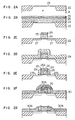
- Figs. 1A to 1L are sectional views showing fabrication steps of an embodiment of a method of fabricating a semiconductor device in accordance with the present invention, more particularly, steps of a fabrication method of bipolar transistor.
- an N-type monocrystalline semiconductor layer 1 (for example, an N-type monocrystalline silicon layer) is first prepared, and a relatively thick insulating layer 2 made of silicon oxide SiO2 is formed locally on a main surface of the semiconductor layer 1 so as to intrude partially into the semiconductor layer.
- an insulating layer 3 made of silicon oxide and having a thickness of, for example, 200 ⁇ is formed on the main surface of the semiconductor layer 1 by the ordinary thermal oxidation process.
- boron ions B+ are implanted into the semiconductor layer 1 through the insulating layer 3 and heat treatment is carried out, to form a P-type monocrystalline semiconductor layer (that is, an intrinsic base region) 4 in the semiconductor layer 1.
- a polycrystalline silicon film 5 which may be doped to be conductive as in the following embodiment and has a thickness of about 5,000 ⁇ is deposited on the insulating layers 2 and 3, a silicon nitride film 6 having a thickness of about 500 ⁇ is deposited on the polycrystalline silicon film 5, and a polycrystalline silicon film 7 containing an N-type impurity such as arsenic at a concentration of, for example, 1x10²¹ atoms/cm3 is deposited on the silicon nitride film 6 to a thickness of about 2,000 ⁇ .
- Each of the films 5, 6 and 7 is formed by, for example, chemical vapor deposition.
- the three-layer film made up of the polycrystalline silicon film 5, the silicon nitride film 6 and the polycrystalline silicon film 7 is etched through photo-etching techniques and RIE techniques so that the three-layer film having a desired shape is left unetched as shown in Fig. 1C.
- a silicon oxide film 8 having a thickness of about 4,000 ⁇ is formed by, for example, chemical vapor deposition. Then, the silicon oxide film 8 is etched through RIE techniques so that, as shown in Fig. 1E, an insulating layer 9 having a width of about 4,000 ⁇ in a lateral direction is left on the side wall of the three-layer film 5, 6 and 7. By the above etching process, the surface 7A of the polycrystalline silicon film 7 and a surface area 4A of the P-type monocrystalline semiconductor layer 4 are both exposed.
- a polycrystalline silicon film 10 having a thickness of about 4,000 ⁇ is formed by, for example, chemical vapor deposition, and the structure thus obtained is heat-treated at 950°C in an atmosphere of nitrogen for about 10 minutes to diffuse the arsenic atoms of the polycrystalline silicon film 7 into that portion of the polycrystalline silicon film 10 which exists near the polycrystalline silicon film 7, thereby forming an N-type polycrystalline silicon region 10A.
- the polycrystalline silicon layers 10, 10A and 7 are subjected to the plasma etching using a Cl2 gas or the so-called photo-excitation etching using chlorine radicals which are obtained by irradiating Cl2 gas with, for example, ultraviolet rays from a low pressure mercury vapor lamp.
- Cl2 gas a Cl2 gas
- the poly crystalline silicon layers 10A and 7 which are doped highly with arsenic, are selectively etched off in a selfalignment manner, and the remaining portion 10B of the polycrystalline silicon film 10 is left unetched in a state that the remaining polycrystalline silicon layer 10B may have two portions separated by the silicon nitride film 6 and the insulating layer 9.
- FIG. 3 shows a relation between the impurity concentration of polycrystalline silicon and the etching rate of the plasma etching or photo-excitation etching (each using Cl2 gas) for polycrystalline silicon.
- the etching rate for polycrystalline silicon containing arsenic at a concentration more than 1020 atoms/cm3 is tens of times larger than the etching rate for polycrystalline silicon which does not contain arsenic.
- polycrystalline silicon containing arsenic can be readily etched off while leaving undoped polycrystalline silicon unetched.
- the polycrystalline silicon layer 10B is patterned through photo-etching techniques and RIE techniques so that the polycrystalline silicon layer 10B exists between the insulating layer 9 and a surface area of the insulating layer 2, and then the structure thus obtained is heat-treated at 850°C in a stream of water vapor for 100 minutes, to perform thermal oxidation while using the silicon nitride film 6 as a mask, thereby forming a silicon oxide layer 11 which has a thickness of about 1,400 ⁇ and serves as an insulating layer, at the surface of the polycrystalline silicon layer 10B.
- boron ions B+ are implanted into the silicon layer 10B at an implant voltage of 60 KV and a dose of 5 x 10¹⁵ atoms/cm2, and then predetermined heat treatment is carried out.
- the polycrystalline silicon layer 10B has the P-type conductivity, and a highly-doped P-type monocrystalline semiconductor layer (namely, an extrinsic base region) 12 is formed in that portion of the P-type monocrystalline semiconductor layer 4 which is kept in contact with the polycrystalline silicon layer 10B.
- the film 5 and the insulating layer 3 act as a mask for preventing boron from diffusing into that portion of the monocrystalline silicon layer 4 which exists under the film 5.
- the above ion implantation and heat treatment may be carried out before the insulating layer 11 is formed.
- the silicon nitride film 6 is removed by, for example, hot phosphoric acid, and then the polycrystalline silicon film 5 is removed by, for example, the plasma etching using a CCl4 gas.
- the oxide film 3 can serve as an etching stopper for preventing etching of the underlying monocrystalline silicon layer 4.
- the insulating layer 3 having a thickness of 200 ⁇ is removed by, for example, an aqueous solution of hydrogen fluoride, to form a window or an aperture 13 as shown in Fig. 1I.
- a polycrystalline silicon film 14 having a thickness of 3,000 ⁇ is formed by, for example, chemical vapor deposition. Then, for example, arsenic ions As+ are implanted into this polycrystalline silicon film at an implant voltage of 60 KV and a dose rate of 1 x 10¹⁶ atoms/cm2, and predetermined heat treatment is carried out.
- the polycrystalline silicon film 14 thus treated is patterned through photo-etching techniques and RIE techniques so that at least the aperture 13 is covered by a polycrystalline silicon layer 14 left unetched.
- the polycrystalline silicon layer 14 has the N-type conductivity, and as shown in Fig. 1J, an N-type monocrystalline semiconductor layer (namely, an emitter region) 15 is formed in that portion of the P-type semiconductor layer 4 which is kept in contact with the polycrystalline silicon layer 14.
- a silicon oxide film (not shown) is deposited on the whole surface, and a phosphosilicate glass film 16 is deposited on the silicon oxide film.
- a phosphosilicate glass film 16 is deposited on the silicon oxide film.
- Each of these films if formed by, for example, chemical vapor deposition.
- the phosphosilicate glass film 16 is subjected to photo-etching and RIE, to form apertures 17 and 18 in those portions of the phosphosilicate glass film which exist on the N-type polycrystalline silicon layer 14 and the P-type polycrystalline silicon layer 10B, thereby exposing a surface area of each of the layers 14 and 10B.
- a conductive film is deposited on the whole surface, for example, by sputtering, and then subjected to photo-etching and RIE as shown in Fig. 1L, to form an electrode 19 which is kept in contact with the layer 14 and extended to the surface of the phosphosilicate glass film 16 through the aperture 17, and an electrode 20 which is kept in contact with the layer 10B and extended to the surface of the phosphosilicate glass film 16 through the aperture 18.
- a bipolar transistor which is fabricated by the present embodiment and is shown in Fig. 1L is an NPN transistor in which the semiconductor layers 4 and 12 are used as a base region, the layer 15 is used as an emitter region, and the remaining portion of the semiconductor layer 1 is used as a collector region.
- the layers 4 and 12 serving as the base region is connected to the electrode 20 (namely, a base electrode) through the layer 10B, and the layer 15 serving as the emitter region is connected to the electrode 19 (namely, an emitter electrode) through the layer 14.
- the base electrode 20 is kept in contact with the polycrystalline silicon layer 10B which is extended from the base region 12 and 4, the area of the layer 12 can be made small, and thus the capacitance of the junction between the collector and base of the bipolar transistor can be reduced. Further, the distance between the emitter region 15 and the highly-doped P-type base layer 12 can be made smaller than the width of the insulating layer 9 in the lateral direction, that is, the layer 12 can be provided in close proximity to the emitter region 15. Accordingly, the base resistance can be reduced, and the transistor can show excellent high-frequency characteristics.
- the present embodiment not only the advantages such as a reduction in junction capacitance and a decrease in base resistance are enhanced, but also the drawback of formation of damaged layer in the emitter region 15 or base region 4 can be completely prevented.
- the etching action for the film 5 can be substantially stopped at the surface of the silicon oxide layer 3 because the etching rate for silicon oxide is far smaller than that for polycrylstalline silicon. Accordingly, in the above etching process, the damaged layer is not formed in the emitter region 15 and the base region 4.
- the silicon oxide layer 3 is very thin, and hence can be readily removed by, for example, the wet etching using an aqueous solution of hydrogen fluoride, without causing damage to the regions 15 and 4.
- a bipolar transistor having desired characteristics can be readily formed and produced at a high yield rate.
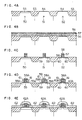
- Figs. 2A to 2J are sectional views showing fabrication steps of a method of fabricating a semiconductor device more specifically an N-channel MOSFET according to another embodiment of the present invention.
- a P-type monocrystalline semiconductor layer 21 made of, for example, P-type monocrystalline silicon is first prepared, and a thick insulating layer 22 made of silicon oxide is formed locally in a main surface of the semiconductor layer 21 so as to form a LOCOS structure partially intruding into the semiconductor layer 21. Then, a silicon oxide layer 23 having a thickness of, for example, 200 ⁇ is formed on the main surface of the semiconductor layer 21 by the ordinary thermal oxidation process, to be used as a gate insulating layer.
- a phosphorus-doped polycrystalline silicon film 24 is deposited on the whole surface, a silicon nitride film 25 having a thickness of about 500 ⁇ is deposited on the film 24, and a polycrystalline silicon film 26 containing an N-type impurity such as arsenic at a concentration of about 1 x 10²¹ atoms/cm3 is deposited on the silicon nitride film 25 to a thickness of about 2,000 ⁇ .
- Each of the films 24, 25 and 26 is formed by, for example, chemical vapor deposition.
- a three-layer film made up of the polycrystalline silicon film 24, the silicon nitride film 25 and the polycrystalline silicon film 26 is subjected to photo-etching and RIE (namely, reactive ion etching) to leave the three-layer film of a desired shape unetched, as shown in Fig. 2C, and then the ion implantation is carried out while using the three-layer film as a mask, to form lightly-doped N-type source and drain regions 27.
- photo-etching and RIE namely, reactive ion etching
- a silicon oxide film 28 having a thickness of 3,500 ⁇ is formed as shown in Fig. 2D by, for example, chemical vapor deposition. Then, the silicon oxide film 28 is etched through RIE techniques so that, as shown in Fig. 2E, an insulating layer 29 having a width of about 3,500 ⁇ in a lateral direction is left on the side wall of the three-layer film 24, 25 and 26. By this etching process, the surface 26A of the polycrystalline silicon film 26 and a surface area 27A of each of the source and drain regions 27 are exposed.
- a polycrystalline silicon film 30 having a thickness of about 3,500 ⁇ is formed as shown in Fig. 2F by, for example, chemical vapor deposition, and the structure thus obtained is heat-treated at 950°C in an atmosphere of nitrogen for about 10 minutes.
- arsenic atoms contained in the polycrystalline silicon film 26 are diffused into that portion of the polycrystalline silicon film 30 which is in contact to or contiguous to the film 26, to form an N-type polycrystalline silicon region 30A in the film 30.
- the layer 30A, the remaining portion of the film 30, and the film 26 are subjected to either the plasma etching using a Cl2 gas or the so-called photo-excitation etching using Cl radials which are obtained by irradiating Cl2 gas with, for example, ultraviolet rays from a low pressure mercury vapor lamp.
- the film 26 and the layer 30A which are doped highly with arsenic are selectively etched off in a self-alignment manner, and the remaining portions of the film 30, that is, two polycrystalline silicon layers 30B are left unremoved and are separated by the silicon nitride film 25 and the insulating layer 29.
- the plasma etching method and the photo-excitation method each utilizing Cl2 gas have the etching characteric shown in Fig. 3. Hence, only the film 26 and the layer 30A which contain arsenic, are selectively etched off by one of the above methods, and the undoped layer 10B is left unetched.
- the polycrystalline silicon layer 30B is etched through photo-etching techniques and RIE techniques so that the polycrystalline silicon layers 30B left unetched are extended from the insulating layer 29 to the surface of the insulating layer 22.
- aresnic ions As+ are implanted into the polycrystalline silicon layers 30B at an implant voltage of 60 KV and a dose rate of 1 x 10¹⁶ atoms/cm2 and predetermined heat treatment is carried out, to convert the layer 30B into an N-type polycrystalline silicon layer 31 and to form highly-doped N-type source and drain regions 32 in the lightly-doped N-type source and drain regions 27.
- a silicon oxide film (not shown) is deposited on the whole surface, and a phosphosilicate glass film 33 is deposited on the above silicon oxide film.
- a phosphosilicate glass film 33 is deposited on the above silicon oxide film.
- Each of these films is formed by, for example, chemical vapor deposition.
- the phosphosilicate glass film 33 is subjected to photo-etching and RIE, to form apertures 34 in the film 33 as shown in Fig. 2I, thereby exposing desired surface areas of the polycrystalline silicon layer 31.
- the nitride film 25 is also at least partially and preferably totally removed to expose the polycrystalline layer 24.
- a conductive film is formed, for example, by sputtering, and then etched through photo-etching techniques and RIE techniques so that electrodes 35 are left as shown in Fig. 2J, that is, each of the electrodes 35 is kept in contact with the polycrystalline silicon layer 31 and extended to the surface of the phosphosilicate glass film 33 through the aperture 34. Also, a gate electrode contacting the doped polycrystalline layer 24 is formed.
- the N-type polycrystalline silicon layers 30A and 26 are selectively etched off by one of the plasma etching and the photo-excitation etching each utilizing a Cl2 gas, the layers 30A and 26 are uniformly etched, and moreover the etching action is surely stopped at the surface of the silicon nitride film 25 and the surface of the insulating layer 29 made of silicon oxide, because the etching rate for silicon nitride and silicon oxide is far smaller than that for N-type polycrystalline silicon. Accordingly, the polycrystalline silicon film 24 (serving as a gate electrode) and the gate insulating layer 23 are not damaged by the above etching process.
- the LDD structure (namely, lightly doped domain structure) for lessening the so-called “short channnel effect" and for preventing the injection of hot carriers into a gate region can be formed, without using any special process.
- an MOSFET having desired characteristics can be readily obtained.
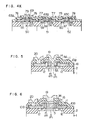
- Figs. 4A to 4K are sectional views showing fabrication procedures of a composite semiconductor which includes a bipolar transistor and a complementary MOS (namely, the combination of an N-channel MOSFET and a P-channel MOSFET) formed on the same substrate.
- N-type monocrystalline semiconductor layers 50 and 52 and a P-type monocrystalline semiconductor layer 51 are first formed in a main surface of a semiconductor substrate, and a thick insulating layer 53 made of silicon oxide is formed locally on the main surface so as to intrude in the semiconductor layers 50, 51 and 52. Then, an insulating layer 54 made of silicon oxide and having a thickness of, for example, 150 ⁇ is formed on the main surface by the ordinary thermal oxidation process. Further, boron ions B+ are implanted into the semiconductor layer 50 through the insulating layer 54 and heat treatment is carried out, to form a P-type monocrystalline semiconductor layer (namely, an intrinsic base region) 55 in the N-type layer 50.
- a phosphorus-doped polycrystalline silicon film 56 having a thickness of 4,000 ⁇ is deposited on the whole surface
- a silicon nitride film 57 having a thickness of 500 ⁇ is deposited on the film 56
- a polycrystalline silicon film 58 containing an N-type impurity such as arsenic at a concentration of, for example, 1 x 10²¹ atoms/cm3 is deposited on the silicon nitride film 57 to a thickness of about 2,000 ⁇ .
- Each of the films 56, 57 and 58 is formed by, for example, chemical vapor deposition.
- a three-layer film made up of the polycrystalline silicon film 56, the silicon nitride film 57 and the polycrystalline silicon film 58 is subjected to photo-etching and RIE (namely, reactive ion etching), to form a pattern shown in Fig. 4C.
- RIE reactive ion etching
- ion implanation is carried out while using the three-layer film as a mask, to form lightly-doped N-type source and drain regions 59 in the semiconductor layer 51 and to form lightly-doped P-type source and drain regions 60 in the semiconductor layer 52.
- a silicon oxide film having a thickness of 3,000 ⁇ is formed on the whole surface by, for example, chemical vapor deposition, and is then etched through photo-etching techniques and RIE techniques so that, as shown in Fig. 4D, an insulating layer 61 having a width of about 3,000 ⁇ in a lateral direction is left on the side wall of the three-layer film 56, 57 and 58.
- the surface 58A of the polycrystalline silicon film 58, a surface area 55A of the semiconductor layer 55, the surface 59A of the source and drain regions 59, and the surface 60A of the source and drain regions 60 are all exposed by the above etching process.
- a polycrystalline silicon film 62 having a thickness of about 4,000 ⁇ is formed by, for example, chemical vapor deposition, and the structure thus obtained is maintained at 950°C in an atmosphere of nitrogen for about 10 minutes, to diffuse arsenic atoms of the polycrystalline silicon film 58 into that portion of the polycrystalline silicon film 62 which is contiguous to the film 58, thereby forming an N-type polycrystalline silicon layer 62A.
- the polycrystalline silicon layers 62, 62A and 58 are subjected to the plasma etching using Cl2 gas or the so-called photoexcitation etching using Cl radicals which are obtained by irradiating a Cl2 gas with, for example, ultraviolet rays from a low pressure mercury vapor lamp.
- Cl2 gas or the so-called photoexcitation etching using Cl radicals which are obtained by irradiating a Cl2 gas with, for example, ultraviolet rays from a low pressure mercury vapor lamp.
- the polycrystalline silicon layer 62A and polycrystalline silicon film 58 which are doped highly with arsenic, are selectively etched off in a selfalignment manner, and the remaining portion of the polycrystalline silicon film 62, that is, an undoped polycrystalline silicon layer 62B is left unetched in a state that the layer 62B is separated into parts by the silicon nitride film 57 and the insulating layer 61.
- the polycrystalline silicon layer 62B is etched into such a pattern, for example, through photoetching techniques that the polycrystalline silicon layer 62B left unetched is extended from the insulating layer 61 to the surface of the insulating layer 53 as shown in Fig. 4G. Then, the structure thus obtained is maintained at 850°C in a stream of water vapor for 80 minutes, to form an insulating layer 64 which is made of silicon oxide and has a thickness of about 1,200 ⁇ , at the surface of the polycrystalline silicon layer 62B.
- the silicon nitride film 57 acts as a mask for preventing the oxidation of the polycrystalline silicon film 56.
- ion implantation is carried out in the fillowing manner.
- boron ions B+ are implanted into those portions of the polycrystalline silicon layer 62B which exist on the semiconductor layers 50 and 52, at an implant voltage of 50 KV and a dose rate of 5 x 10¹⁵ atoms/cm2, and arsenic ions As+ are implanted into that portion of the polycrystalline silicon film 62B which exists on the semiconductor layer 51, at an implant voltage of 260 KV and a dose rate of 1 x 10¹⁶ atoms/cm2.
- predetermined heat treatment is carried out.
- P-type polycrystalline silicon layers 63A and 63C, a highly-doped P-type extrinsic base region 65, and highly-doped P-type source and drain regions 67 are formed.
- an N-type polycrystalline silicon layer 63B and highly-doped N-type source and drain regions 66 are formed.
- the silicon nitride film 57 and the polycrystalline silicon film 56 which exist over the semiconductor layer 50 are removed through photo-etching techniques and RIE techniques using the insulating layer 54 as an etching stopper, and the insulating layer 54 which exists on the semiconductor layer 50 and has a thickness of 150 ⁇ , is removed by, for example, an aqueous solution of hydrogen fluoride, to form an aperture 68 as shown in Fig. 4H.
- a polycrystalline silicon film 69 having a thickness of 2,000 ⁇ is formed by, for example, chemical vapor deposition.
- arsenic ions As+ are implanted into the above polycrystalline silicon film at an implant voltage of 60 KV and a dose rate of 1 x 10¹⁶ atoms/cm2, and predetermined heat treatment is carried out.
- the polycrystalline silicon film thus treated is etched through photo-etching techniques and RIE techniques into such a pattern that at least the aperture 68 is covered by the polycrystalline silicon film left unetched.
- an N-type polycrystalline silicon layer 69 is formed, and an N-type monocrystalline semiconductor layer 70 serving as an emitter region is formed in that portion of the semiconductor layer 55 which exists near the polycrystalline silicon layer 69.
- the silicon nitride film 57 existing over each of the semiconductor layers 51 and 52 is removed by, for example, hot phosphoric acid.
- a silicon oxide film (not shown) is deposited on the whole surface, and a phosphosilicate glass film 71 is deposited on the above silicon oxide film.
- Each of these films is formed by, for example, chemical vapor deposition.
- Those portions of the phosphosilicate glass film 71 which exist on the polycrystalline silicon layers 63A, 63B, 63C and 69, are etched through photo-etching techniques and RIE techniques, to form apertures 72 to 75 as shown in Fig. 4J, thereby exposing a surface area of each of the layers 63A, 63B, 63C and 69.
- a conductive film is formed on the whole surface, for example, by sputtering, and then etched through photo-etching techniques and RIE techniques so that electrodes 76 to 79 are left unetched as shown in Fig. 4K.
- the electrode 76 of for example aluminium or silicide of refractory metal kept in contact with the layer 63A is extended to the surface of the phosphosilicate glass film 71 through the aperture 72
- the electrode 77 kept in contact with the layer 63B is extended to the surface of the glass film 71 through the aperture 73
- the electrode 78 kept in contact with the layer 63C is extended to the surface of the glass film 71 through the aperture 74
- the electrode 79 kept in contact with the layer 69 is extended to the surface of the glass film 71 through the aperture 75.
- the semiconductor device of Fig. 4K fabricated by the present embodiment includes an NPN transistor in which the regions 55 and 65 are used as a base region, the region 70 is used as an emitter region, and the remaining portion of the semiconductor layer 50 is used as a collector region, an N- channel MOSFET in which a set of regions 59 and 66 is used as a source region, another set of regions 59 and 66 is used as a drain region, and the film 56 is used as a gate, and a P-channel MOSFET in which a set of regions 60 and 67 is used as a source region, another set of regions 60 and 67 is used as a drain region, and the film 56 is used as a gate.
- the regions 65, 66 and 67 are connected to the electrodes 76, 77 and 78 through the layers 63A, 63B and 63C, respectively. Accordingly, the area of each of the regions 65, 66 and 67 can be reduced, in size as compared with a case where the electrodes 76, 77 and 78 are connected directly with the regions 65, 66 and 67, respectively, without using intervening layers 63A, 63B and 63C. Thus, the junction capacitance between the collector and base of the NPN transistor and the junction capacitance at each of the source and drain regions of the N-channel or P-channel MOSFET can be reduced.
- the distance between the emitter region 70 and the extrinsic base region 65 can be readily made smaller than the width of the insulating layer 61 in the lateral direction, and hence the base resistance can be greatly reduced.
- the silicon oxide layer 54 acts as a protective film, and the monocrystalline silicon layer 55 is not damaged.
- the LDD structure for lessening the so-called "short channel effect" and for preventing the injection of hot carriers into a gate region can be readily formed in each of the N-channel and P-channel MOSFET's.
- a composite semiconductor device which includes a bipolar transistor and a complementary MOS and has excellent high-frequency characteristics, can be readily formed and produced at a high yield.
- the polycrystalline silicon film 56 is used as the gate, by way of example.
- the gate may be made of the silicide of a refractory metal such as tungsten silicide WSi2 and titanium silicide TiSi2.
- Fig. 5 shows a modified version of the bipolar transistor shown in Fig. 1L. Accordingly, the following explanation of the present embodiment will be limited to fabrication steps concerning a transistor part, in which the transistor of Fig. 5 is different from the transistor of Fig. 1L.
- an insulating layer 9A which is made of silicon oxide and has a width of, for example, 1,500 ⁇ in the lateral direction, is formed on the side wall of the three-layer film 5, 6 and 7 in the steps of Figs. 1D and 1E. Further, when the film 5 is etched in the step of Fig.
- anisotropic etching is carried out by, for example, the RIE method, to leave that portion of the film 5 which exists in the neighborhood of the insulating layer 9A, unetched.
- a polycrystalline silicon layer 5A having a width of 2,500 ⁇ in the lateral direction is left on the side wall of the insulating layer 9A.
- That portion of the insulating layer 3 which is not covered by the layer 5A, that is, an exposed portion of the insulating layer 3 is etched off by, for example, an aqueous solution of hydrogen fluoride, to expose a surface area of the semiconductor layer 4.
- substantially the same processing as shown in Figs. 1J to 1L is carried out, and thus the NPN transistor of Fig. 5 is fabricated.
- the width of the emitter region 15 in the lateral direction can be made smaller than the lateral width of the three-layer film 5, 6 and 7 of Fig. 1C determined by the size of a mask which is used for leaving the above three-layer film unetched. Accordingly, the lateral width of the intrinsic base region 4 existing beneath the emitter region 15 can be reduced, and thus the base resistance can be made smaller than that of the transistor of Fig. 1L. That is, a bipolar transistor having more excellent high-frequency characteristics can be fabricated by the present embodiment.
- Fig. 6 shows another modified version of the bipolar transistor shown in Fig. 1L. Accordingly, the following explanation of the present embodiment will be limited to fabrication steps concerning a transistor part, in which the transistor of Fig. 6 is different from the transistor of Fig. 1L.
- the insulating layer 3 is removed.
- the silicon nitride film 6 is deposited to a thickness of, for example, 2,000 ⁇ .
- boron ions B+ are implanted into the semiconductor layer 4.
- the silicon nitride film 6 is used as a mask. Then, predetermined heat treatment is carried out, to form the region 12. Thereafter, the insulating layer 11 made of silicon oxide is formed. In the step of Fig. 1I, only the silicon nitride film 6 is removed. Thereafter, substantially the same processing as shown in Figs. 1J to 1K is carried out, to form an NPN transistor. Like the embodiment shown in Figs. 1A to 1L, the present embodiment can eliminate the drawback of the prior art.
- Fig. 7 shows a modified version of the MOSFET shown in Fig. 2J. Accordingly, the following explanation of the present embodiment will be limited to fabrication steps concerning a part, in which the MOSFET of Fig. 7 is different from that of Fig. 2J.
- an insulating layer 31 ⁇ made of silicon oxide is deposited on the layer 31.
- the silicon nitride film 25 is used as a mask. Then, the silicon nitride film 25 is removed.
- a phosphorus-doped polycrystalline silicon film 24 ⁇ is formed so as to cover the film 24 and to be extended to the surface of the insulating layer 31 ⁇ .
- an aperture is formed in the phosphosilicate glass film 33 at a position on the layer 24 ⁇ .
- An electrode 36 is formed so as to fill up this aperture.
- an N-channel MOSFET is fabricated.
- the area of MOSFET can be reduced, as compared with a case where the polycrystalline silicon film 24 is extended to a position existing over the insulating layer 22, and a gate electrode is formed on the film 24 at this position, since the electrode 36 is provided on the polycrystalline silicon film 24 ⁇ which exists over the insulating layer 23.
- FIG. 8 shows another modified version of the MOSFET shown in Fig. 2J.
- the following explanation of the present embodiment will be limited to fabrication steps concerning a part, in which the MOSFET shown in Fig. 8 is different from that shown in Fig. 2J.
- an insulating layer 31 ⁇ made of silicon oxide is formed on the layer 31.
- the silicon nitride film 25 is used as a mask. Then, the films 24 and 25 are removed.
- a phosphorus-doped polycrystalline silicon film 24 ⁇ is formed so as to cover the insulating layer 23 and to be extended to the surface of the insulating layer 31 ⁇ .
- an aperture is formed in the phosphosilicate glass film 33 at a position on the layer 24 ⁇ , and an electrode 36 is formed so as to fill up the aperture.
- an N-channel MOSFET is formed.
- the present embodiment has the same advantages as the embodiment which has been explained by reference to Fig. 7.
- a bipolar transistor and an MOSFET can be readily formed on the same substrate by combining one of the above fabrication methods of bipolar transistor with one of the above fabrication methods of MOSFET.
- a composite semiconductor device can be readily formed which includes a bipolar transistor and an MOSFET, and has excellent high-frequency characteristics.
- the junction capacitance between the base and collector of a bipolar transistor can be made small, and the base resistance thereof can be reduced. Further, in the fabrication process, there is no danger of damage to the monocrystalline emitter and base regions. That is, a bipolar transistor having excellent high-frequency characteristics can be readily formed and produced at a high yield.
- the junction capacitance at each of the source and drain regions of an MOSFET can be reduced, and moreover the LDD structure for lessening the short channel effect can be readily formed.
- an MOSFET having excellent high-frequency characteristics can readily formed and produced at a high yield.
- some main steps of the fabrication method of the above bipolar transistor are compatible with those of the fabrication method of the above MOSFET, and hence a composite semiconductor device which is made up of the bipolar transistor and the MOSFET and has excellent high-frequency characteristics, can be readily formed and produced at a high yield.
Landscapes
- Bipolar Transistors (AREA)
- Metal-Oxide And Bipolar Metal-Oxide Semiconductor Integrated Circuits (AREA)
Applications Claiming Priority (2)
| Application Number | Priority Date | Filing Date | Title |
|---|---|---|---|
| JP61159631A JPH0628266B2 (ja) | 1986-07-09 | 1986-07-09 | 半導体装置の製造方法 |
| JP159631/86 | 1986-07-09 |
Publications (3)
| Publication Number | Publication Date |
|---|---|
| EP0252206A2 true EP0252206A2 (de) | 1988-01-13 |
| EP0252206A3 EP0252206A3 (en) | 1988-08-31 |
| EP0252206B1 EP0252206B1 (de) | 1992-07-15 |
Family
ID=15697933
Family Applications (1)
| Application Number | Title | Priority Date | Filing Date |
|---|---|---|---|
| EP87101113A Expired EP0252206B1 (de) | 1986-07-09 | 1987-01-27 | Verfahren zum Herstellen einer Halbleiterstruktur |
Country Status (4)
| Country | Link |
|---|---|
| US (1) | US4735916A (de) |
| EP (1) | EP0252206B1 (de) |
| JP (1) | JPH0628266B2 (de) |
| DE (1) | DE3780369T2 (de) |
Cited By (10)
| Publication number | Priority date | Publication date | Assignee | Title |
|---|---|---|---|---|
| EP0346543A1 (de) * | 1988-06-15 | 1989-12-20 | BRITISH TELECOMMUNICATIONS public limited company | Bipolarer Transistor |
| EP0346535A1 (de) * | 1987-02-27 | 1989-12-20 | BRITISH TELECOMMUNICATIONS public limited company | Selbstausrichtendes bipolares Herstellungsverfahren |
| GB2220102A (en) * | 1988-06-27 | 1989-12-28 | Seiko Epson Corp | "Method of making a bipolar transistor" |
| GB2193036B (en) * | 1986-07-24 | 1990-05-02 | Mitsubishi Electric Corp | Method of fabricating a semiconductor integrated circuit device |
| EP0450376A1 (de) * | 1990-04-02 | 1991-10-09 | National Semiconductor Corporation | BiCMOS-Bauelement mit engbenachbarten Kontakten und dessen Herstellungsverfahren |
| DE4123436A1 (de) * | 1991-04-09 | 1992-10-15 | Samsung Electronics Co Ltd | Halbleitervorrichtung und verfahren zur herstellung derselben |
| EP0437306A3 (en) * | 1990-01-12 | 1993-03-31 | Paradigm Technology, Inc. | Self-aligning contact and interconnect structure |
| US5234847A (en) * | 1990-04-02 | 1993-08-10 | National Semiconductor Corporation | Method of fabricating a BiCMOS device having closely spaced contacts |
| US5656861A (en) * | 1990-01-12 | 1997-08-12 | Paradigm Technology, Inc. | Self-aligning contact and interconnect structure |
| WO2006109221A3 (en) * | 2005-04-13 | 2007-03-29 | Koninkl Philips Electronics Nv | Lateral bipolar transistor |
Families Citing this family (36)
| Publication number | Priority date | Publication date | Assignee | Title |
|---|---|---|---|---|
| JPS63184364A (ja) * | 1987-01-27 | 1988-07-29 | Toshiba Corp | 半導体装置の製造方法 |
| US4826782A (en) * | 1987-04-17 | 1989-05-02 | Tektronix, Inc. | Method of fabricating aLDD field-effect transistor |
| US4902640A (en) * | 1987-04-17 | 1990-02-20 | Tektronix, Inc. | High speed double polycide bipolar/CMOS integrated circuit process |
| JPS63268258A (ja) * | 1987-04-24 | 1988-11-04 | Nec Corp | 半導体装置 |
| US4829025A (en) * | 1987-10-02 | 1989-05-09 | Advanced Micro Devices, Inc. | Process for patterning films in manufacture of integrated circuit structures |
| US5017995A (en) * | 1987-11-27 | 1991-05-21 | Nec Corporation | Self-aligned Bi-CMOS device having high operation speed and high integration density |
| US5225355A (en) * | 1988-02-26 | 1993-07-06 | Fujitsu Limited | Gettering treatment process |
| JP2727557B2 (ja) * | 1988-03-25 | 1998-03-11 | ソニー株式会社 | 半導体装置の製造方法 |
| JPH0223648A (ja) * | 1988-07-12 | 1990-01-25 | Seiko Epson Corp | 半導体装置 |
| US5015594A (en) * | 1988-10-24 | 1991-05-14 | International Business Machines Corporation | Process of making BiCMOS devices having closely spaced device regions |
| JP2918205B2 (ja) * | 1988-11-09 | 1999-07-12 | 三菱電機株式会社 | 半導体装置およびその製造方法 |
| US5079180A (en) * | 1988-12-22 | 1992-01-07 | Texas Instruments Incorporated | Method of fabricating a raised source/drain transistor |
| US4945070A (en) * | 1989-01-24 | 1990-07-31 | Harris Corporation | Method of making cmos with shallow source and drain junctions |
| US5238857A (en) * | 1989-05-20 | 1993-08-24 | Fujitsu Limited | Method of fabricating a metal-oxide-semiconductor device having a semiconductor on insulator (SOI) structure |
| JPH03141645A (ja) * | 1989-07-10 | 1991-06-17 | Texas Instr Inc <Ti> | ポリサイドによる局所的相互接続方法とその方法により製造された半導体素子 |
| US5294822A (en) * | 1989-07-10 | 1994-03-15 | Texas Instruments Incorporated | Polycide local interconnect method and structure |
| US5171702A (en) * | 1989-07-21 | 1992-12-15 | Texas Instruments Incorporated | Method for forming a thick base oxide in a BiCMOS process |
| US5024959A (en) * | 1989-09-25 | 1991-06-18 | Motorola, Inc. | CMOS process using doped glass layer |
| US4960726A (en) * | 1989-10-19 | 1990-10-02 | International Business Machines Corporation | BiCMOS process |
| US5112761A (en) * | 1990-01-10 | 1992-05-12 | Microunity Systems Engineering | Bicmos process utilizing planarization technique |
| US5182225A (en) * | 1990-01-10 | 1993-01-26 | Microunity Systems Engineering, Inc. | Process for fabricating BICMOS with hypershallow junctions |
| US5102816A (en) * | 1990-03-27 | 1992-04-07 | Sematech, Inc. | Staircase sidewall spacer for improved source/drain architecture |
| US5071780A (en) * | 1990-08-27 | 1991-12-10 | Taiwan Semiconductor Manufacturing Company, Ltd. | Reverse self-aligned transistor integrated circuit |
| KR100307272B1 (ko) * | 1990-12-04 | 2002-05-01 | 하라 레이노스케 | Mos소자제조방법 |
| JPH05110005A (ja) * | 1991-10-16 | 1993-04-30 | N M B Semiconductor:Kk | Mos型トランジスタ半導体装置およびその製造方法 |
| KR100281346B1 (ko) * | 1992-04-28 | 2001-03-02 | 칼 하인쯔 호르닝어 | 도핑된 영역내 비아 홀 제조방법 |
| JP2886420B2 (ja) * | 1992-10-23 | 1999-04-26 | 三菱電機株式会社 | 半導体装置の製造方法 |
| US5407841A (en) * | 1992-10-30 | 1995-04-18 | Hughes Aircraft Company | CBiCMOS fabrication method using sacrificial gate poly |
| US5338750A (en) * | 1992-11-27 | 1994-08-16 | Industrial Technology Research Institute | Fabrication method to produce pit-free polysilicon buffer local oxidation isolation |
| US5496750A (en) * | 1994-09-19 | 1996-03-05 | Texas Instruments Incorporated | Elevated source/drain junction metal oxide semiconductor field-effect transistor using blanket silicon deposition |
| FR2756103B1 (fr) * | 1996-11-19 | 1999-05-14 | Sgs Thomson Microelectronics | Fabrication de circuits integres bipolaires/cmos et d'un condensateur |
| US6352899B1 (en) * | 2000-02-03 | 2002-03-05 | Sharp Laboratories Of America, Inc. | Raised silicide source/drain MOS transistors having enlarged source/drain contact regions and method |
| JP4870873B2 (ja) * | 2001-03-08 | 2012-02-08 | ルネサスエレクトロニクス株式会社 | 半導体装置の製造方法 |
| FR2854494A1 (fr) * | 2003-05-02 | 2004-11-05 | St Microelectronics Sa | Procede de fabrication d'un transistor bipolaire |
| US7772653B1 (en) * | 2004-02-11 | 2010-08-10 | National Semiconductor Corporation | Semiconductor apparatus comprising bipolar transistors and metal oxide semiconductor transistors |
| US8999791B2 (en) * | 2013-05-03 | 2015-04-07 | International Business Machines Corporation | Formation of semiconductor structures with variable gate lengths |
Family Cites Families (15)
| Publication number | Priority date | Publication date | Assignee | Title |
|---|---|---|---|---|
| US4127931A (en) * | 1974-10-04 | 1978-12-05 | Nippon Electric Co., Ltd. | Semiconductor device |
| JPS53132275A (en) * | 1977-04-25 | 1978-11-17 | Nippon Telegr & Teleph Corp <Ntt> | Semiconductor device and its production |
| JPS54140483A (en) * | 1978-04-21 | 1979-10-31 | Nec Corp | Semiconductor device |
| US4354309A (en) * | 1978-12-29 | 1982-10-19 | International Business Machines Corp. | Method of manufacturing a metal-insulator-semiconductor device utilizing a graded deposition of polycrystalline silicon |
| US4381953A (en) * | 1980-03-24 | 1983-05-03 | International Business Machines Corporation | Polysilicon-base self-aligned bipolar transistor process |
| JPS56160034A (en) * | 1980-05-14 | 1981-12-09 | Fujitsu Ltd | Impurity diffusion |
| FR2508704B1 (fr) * | 1981-06-26 | 1985-06-07 | Thomson Csf | Procede de fabrication de transistors bipolaires integres de tres petites dimensions |
| US4483726A (en) * | 1981-06-30 | 1984-11-20 | International Business Machines Corporation | Double self-aligned fabrication process for making a bipolar transistor structure having a small polysilicon-to-extrinsic base contact area |
| JPS59161069A (ja) * | 1983-03-04 | 1984-09-11 | Oki Electric Ind Co Ltd | Mos型半導体装置の製造方法 |
| DE3330895A1 (de) * | 1983-08-26 | 1985-03-14 | Siemens AG, 1000 Berlin und 8000 München | Verfahren zum herstellen von bipolartransistorstrukturen mit selbstjustierten emitter- und basisbereichen fuer hoechstfrequenzschaltungen |
| JPS59139678A (ja) * | 1984-01-17 | 1984-08-10 | Hitachi Ltd | 半導体装置 |
| JPH06101475B2 (ja) * | 1984-02-27 | 1994-12-12 | 株式会社日立製作所 | 半導体装置の製造方法 |
| JPS615580A (ja) * | 1984-06-19 | 1986-01-11 | Toshiba Corp | 半導体装置の製造方法 |
| EP0166923A3 (de) * | 1984-06-29 | 1987-09-30 | International Business Machines Corporation | Hochleistungsbipolartransistor mit einem zwischen dem Emitter und der Extrinsic-Basiszone angeordneten leicht dotierten Schutzring |
| EP0170250B1 (de) * | 1984-07-31 | 1990-10-24 | Kabushiki Kaisha Toshiba | Bipolarer Transistor und Verfahren zu seiner Herstellung |
-
1986
- 1986-07-09 JP JP61159631A patent/JPH0628266B2/ja not_active Expired - Lifetime
-
1987
- 1987-01-27 EP EP87101113A patent/EP0252206B1/de not_active Expired
- 1987-01-27 DE DE8787101113T patent/DE3780369T2/de not_active Expired - Fee Related
- 1987-02-10 US US07/013,252 patent/US4735916A/en not_active Expired - Fee Related
Cited By (12)
| Publication number | Priority date | Publication date | Assignee | Title |
|---|---|---|---|---|
| GB2193036B (en) * | 1986-07-24 | 1990-05-02 | Mitsubishi Electric Corp | Method of fabricating a semiconductor integrated circuit device |
| EP0346535A1 (de) * | 1987-02-27 | 1989-12-20 | BRITISH TELECOMMUNICATIONS public limited company | Selbstausrichtendes bipolares Herstellungsverfahren |
| EP0346543A1 (de) * | 1988-06-15 | 1989-12-20 | BRITISH TELECOMMUNICATIONS public limited company | Bipolarer Transistor |
| GB2220102A (en) * | 1988-06-27 | 1989-12-28 | Seiko Epson Corp | "Method of making a bipolar transistor" |
| GB2220102B (en) * | 1988-06-27 | 1992-01-29 | Seiko Epson Corp | Method of making a bipolar transistor |
| EP0437306A3 (en) * | 1990-01-12 | 1993-03-31 | Paradigm Technology, Inc. | Self-aligning contact and interconnect structure |
| US5620919A (en) * | 1990-01-12 | 1997-04-15 | Paradigm Technology, Inc. | Methods for fabricating integrated circuits including openings to transistor regions |
| US5656861A (en) * | 1990-01-12 | 1997-08-12 | Paradigm Technology, Inc. | Self-aligning contact and interconnect structure |
| EP0450376A1 (de) * | 1990-04-02 | 1991-10-09 | National Semiconductor Corporation | BiCMOS-Bauelement mit engbenachbarten Kontakten und dessen Herstellungsverfahren |
| US5234847A (en) * | 1990-04-02 | 1993-08-10 | National Semiconductor Corporation | Method of fabricating a BiCMOS device having closely spaced contacts |
| DE4123436A1 (de) * | 1991-04-09 | 1992-10-15 | Samsung Electronics Co Ltd | Halbleitervorrichtung und verfahren zur herstellung derselben |
| WO2006109221A3 (en) * | 2005-04-13 | 2007-03-29 | Koninkl Philips Electronics Nv | Lateral bipolar transistor |
Also Published As
| Publication number | Publication date |
|---|---|
| US4735916A (en) | 1988-04-05 |
| DE3780369D1 (de) | 1992-08-20 |
| JPS6316673A (ja) | 1988-01-23 |
| JPH0628266B2 (ja) | 1994-04-13 |
| EP0252206B1 (de) | 1992-07-15 |
| EP0252206A3 (en) | 1988-08-31 |
| DE3780369T2 (de) | 1993-03-04 |
Similar Documents
| Publication | Publication Date | Title |
|---|---|---|
| EP0252206B1 (de) | Verfahren zum Herstellen einer Halbleiterstruktur | |
| EP0173953B1 (de) | Verfahren zum Herstellen einer Halbleiteranordnung mit Gateelektrode | |
| EP0088922B1 (de) | Verfahren zum Herstellen von Elektroden und Verdrahtungsstreifen auf einer Halbleiteranordnung | |
| KR100445904B1 (ko) | 소스 필드 플레이트를 갖는 드레인 확장형 모스 전계 효과트랜지스터 및그 제조방법 | |
| JP2605008B2 (ja) | 半導体装置の製造方法 | |
| US4873557A (en) | MIS FET and process of fabricating the same | |
| US4545114A (en) | Method of producing semiconductor device | |
| US4757032A (en) | Method for DMOS semiconductor device fabrication | |
| US4782030A (en) | Method of manufacturing bipolar semiconductor device | |
| KR19980033385A (ko) | 측면 방향 게터링을 이용한 반도체 장치 제조 방법 | |
| KR20010007124A (ko) | 이중 작용 기능 도핑 및 보호 절연 캡을 제공하는 방법 | |
| EP0369336A2 (de) | Prozess zur Herstellung von Bipolar- und CMOS-Transistoren auf einem gemeinsamen Substrat | |
| US5028554A (en) | Process of fabricating an MIS FET | |
| EP0401786B1 (de) | Verfahren zur Herstellung eines lateralen Bipolartransistors | |
| KR0172262B1 (ko) | 반도체 소자의 제조방법 | |
| US5045493A (en) | Semiconductor device and method of manufacturing the same | |
| US5705437A (en) | Trench free process for SRAM | |
| JP2908715B2 (ja) | モスフェット(mosfet)及びその製造方法 | |
| US6451645B1 (en) | Method for manufacturing semiconductor device with power semiconductor element and diode | |
| US5994196A (en) | Methods of forming bipolar junction transistors using simultaneous base and emitter diffusion techniques | |
| EP0242893B1 (de) | Verfahren zur Herstellung einer Halbleiteranordnung | |
| US5747374A (en) | Methods of fabricating bipolar transistors having separately formed intrinsic base and link-up regions | |
| JPH08181327A (ja) | 薄膜トランジスタ及びその製造方法 | |
| JP2633104B2 (ja) | 半導体装置の製造方法 | |
| KR0170436B1 (ko) | 모스트랜지스터 제조방법 |
Legal Events
| Date | Code | Title | Description |
|---|---|---|---|
| PUAI | Public reference made under article 153(3) epc to a published international application that has entered the european phase |
Free format text: ORIGINAL CODE: 0009012 |
|
| AK | Designated contracting states |
Kind code of ref document: A2 Designated state(s): DE FR GB |
|
| PUAL | Search report despatched |
Free format text: ORIGINAL CODE: 0009013 |
|
| AK | Designated contracting states |
Kind code of ref document: A3 Designated state(s): DE FR GB |
|
| 17P | Request for examination filed |
Effective date: 19880905 |
|
| 17Q | First examination report despatched |
Effective date: 19901211 |
|
| GRAA | (expected) grant |
Free format text: ORIGINAL CODE: 0009210 |
|
| AK | Designated contracting states |
Kind code of ref document: B1 Designated state(s): DE FR GB |
|
| REF | Corresponds to: |
Ref document number: 3780369 Country of ref document: DE Date of ref document: 19920820 |
|
| ET | Fr: translation filed | ||
| PLBE | No opposition filed within time limit |
Free format text: ORIGINAL CODE: 0009261 |
|
| STAA | Information on the status of an ep patent application or granted ep patent |
Free format text: STATUS: NO OPPOSITION FILED WITHIN TIME LIMIT |
|
| 26N | No opposition filed | ||
| PGFP | Annual fee paid to national office [announced via postgrant information from national office to epo] |
Ref country code: FR Payment date: 19931129 Year of fee payment: 8 |
|
| PGFP | Annual fee paid to national office [announced via postgrant information from national office to epo] |
Ref country code: GB Payment date: 19940117 Year of fee payment: 8 |
|
| PGFP | Annual fee paid to national office [announced via postgrant information from national office to epo] |
Ref country code: DE Payment date: 19940330 Year of fee payment: 8 |
|
| PG25 | Lapsed in a contracting state [announced via postgrant information from national office to epo] |
Ref country code: GB Effective date: 19950127 |
|
| GBPC | Gb: european patent ceased through non-payment of renewal fee |
Effective date: 19950127 |
|
| PG25 | Lapsed in a contracting state [announced via postgrant information from national office to epo] |
Ref country code: FR Effective date: 19950929 |
|
| PG25 | Lapsed in a contracting state [announced via postgrant information from national office to epo] |
Ref country code: DE Effective date: 19951003 |
|
| REG | Reference to a national code |
Ref country code: FR Ref legal event code: ST |