EP0252654A2 - Speichervorrichtung mit programmierbaren Ausgangsstrukturen - Google Patents
Speichervorrichtung mit programmierbaren Ausgangsstrukturen Download PDFInfo
- Publication number
- EP0252654A2 EP0252654A2 EP87305632A EP87305632A EP0252654A2 EP 0252654 A2 EP0252654 A2 EP 0252654A2 EP 87305632 A EP87305632 A EP 87305632A EP 87305632 A EP87305632 A EP 87305632A EP 0252654 A2 EP0252654 A2 EP 0252654A2
- Authority
- EP
- European Patent Office
- Prior art keywords
- output
- signal
- programmable
- input
- memory
- Prior art date
- Legal status (The legal status is an assumption and is not a legal conclusion. Google has not performed a legal analysis and makes no representation as to the accuracy of the status listed.)
- Withdrawn
Links
- 230000015654 memory Effects 0.000 claims abstract description 14
- 230000006870 function Effects 0.000 claims description 12
- 230000001360 synchronised effect Effects 0.000 claims description 4
- 230000004044 response Effects 0.000 claims 1
- 229940000425 combination drug Drugs 0.000 description 2
- 238000012986 modification Methods 0.000 description 2
- 230000004048 modification Effects 0.000 description 2
- 230000008054 signal transmission Effects 0.000 description 2
- 238000013500 data storage Methods 0.000 description 1
- 239000011159 matrix material Substances 0.000 description 1
- 238000000034 method Methods 0.000 description 1
- 230000005855 radiation Effects 0.000 description 1
- 239000004065 semiconductor Substances 0.000 description 1
- 230000036962 time dependent Effects 0.000 description 1
Images


Classifications
-
- H—ELECTRICITY
- H03—ELECTRONIC CIRCUITRY
- H03K—PULSE TECHNIQUE
- H03K19/00—Logic circuits, i.e. having at least two inputs acting on one output; Inverting circuits
- H03K19/02—Logic circuits, i.e. having at least two inputs acting on one output; Inverting circuits using specified components
- H03K19/173—Logic circuits, i.e. having at least two inputs acting on one output; Inverting circuits using specified components using elementary logic circuits as components
- H03K19/177—Logic circuits, i.e. having at least two inputs acting on one output; Inverting circuits using specified components using elementary logic circuits as components arranged in matrix form
- H03K19/17748—Structural details of configuration resources
- H03K19/1776—Structural details of configuration resources for memories
-
- H—ELECTRICITY
- H03—ELECTRONIC CIRCUITRY
- H03K—PULSE TECHNIQUE
- H03K19/00—Logic circuits, i.e. having at least two inputs acting on one output; Inverting circuits
- H03K19/02—Logic circuits, i.e. having at least two inputs acting on one output; Inverting circuits using specified components
- H03K19/173—Logic circuits, i.e. having at least two inputs acting on one output; Inverting circuits using specified components using elementary logic circuits as components
- H03K19/177—Logic circuits, i.e. having at least two inputs acting on one output; Inverting circuits using specified components using elementary logic circuits as components arranged in matrix form
- H03K19/17704—Logic circuits, i.e. having at least two inputs acting on one output; Inverting circuits using specified components using elementary logic circuits as components arranged in matrix form the logic functions being realised by the interconnection of rows and columns
Definitions
- the present invention relates generally to integrated circuit memory devices with programmable output structure. More particularly, we will describe a programmable read-only memory (PROM) device having separately programmable output modes.
- PROM programmable read-only memory
- PROM programmable read-only memory
- the PROM device internally includes a decoder and an addressable array of gates implementing logical functions in a two-level implementation in sum-of-terms form.
- the decoder generally comprises a fixed AND gate array by which input variables are decoded and output as the terms of a function.
- the addressable array comprises OR gates having special internal links that can be fused or severed to form the required circuit paths that "program" the device according to the specifications of the user.
- the connections between the outputs of the decoder and the inputs of the OR gates can be specified to implement a certain logic program.
- PROM devices for implementing logic functions has certain advantages over other programmable integrated circuit memory devices (such as speed of operation and ability to decode all input combinations), a major drawback has been that the type of outputs is limited to either combinatorial, as shown in FIGURE 1a, or registered, as shown in FIGURE 1b, modes only.
- FIGURE 2a depicts a typical, well-known combinatorial logic-type structure 1.
- the state of the fuse link 3 will control the gate 5 to invert or not to invert a signal on input 7.
- the output 9 is commonly known as a "nonstored” or “nonregistered” signal.
- FIGURE 2b depicts a typical, well-known registered-type structure 11.
- a data storage register 13 has a data input D coupled via line 7 ⁇ to one of the input signals, and an output Q coupled via line 9 ⁇ to one of the single outputs of the circuit or chip.
- the output as shown in FIGURE 1b is commonly known as a "stored” or “registered” signal.
- Combinatorial logic output PROM devices are useful when there is a large number of possible input combinations or product term outputs, whereas registered logic output PROM devices are useful for sequential logic, viz., where there is a large number of variables involved in the logic function.
- a registered PROM device can function as a state machine in which the next output is a function of the present state (stored in the register) and the inputs.
- PROM device which provides the capability of defining and programming the architecture of each output on an individual basis.
- PROM device which can provide either combinatorial or registered output signals.
- PROM device having output components which can be programmed to provide combinatorial or registered output signals, inverted or noninverted, in any combination
- PROM device which has output structures which are individually user programmable.
- the output structure is coupled to the PROM circuit outputs and includes programmable circuitry whereby the user can program the output structure to provide nonstored/nonregistered or stored/registered signals or any combination thereof as the output.
- PROM devices as depicted in FIGURES 1 and 2, and the implementing specific circuitry, are well-known in the art and are described in detail in many publications. See e.g., Handbook of Semiconductor and Bubble Memories , W. A. Triebel and A. E. Chu, Prentice-Hall, Inc., copyright 1982. As such, no detailed discussion is made herein.
- Embodiments of the output structure used in the present invention are described in detail in co-pending, U.S. Patent Application 06/433,253.
- PAL programmable array logic
- PLA programmable logic array
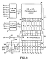
- FIGURE 3 the combination of a PROM structure with a programmable output structure is shown.
- a 2048 x 8 bit PROM device is shown.
- the present invention can be implemented in a multitude of memory size configurations and input/output pin chip carried packages. Therefore, the specific architecture described herein is not to be understood as any specific limitation on the invention, but only as an example of one embodiment of the general inventive concept.
- the PROM section 2 of the exemplary embodiment of the present invention has eleven input lines, A0 - A10.
- A0 - A3 are input to sixteen array column decoder circuit components 4.
- Inputs A4 - A10 are coupled to one hundred twenty-eight array row decoder circuit components 6.
- the memory is, for example, a programmable AND array 8 arranged in a 128 x 128 matrix used to store digital data.
- each row decoder 6 Depending on the binary code address bits applied to the input lines A4 - A10, each row decoder 6 provides a signal to select one of the rows in the array 8 via input lines 10. Each row decoder 6 thus enables a row to be READ.
- the remaining address input bits A0 - A3, are decoded by the column decoders 4.
- the column decoders 4 are used to provide signals to a multiplexer 12 via input lines 14.
- the exemplary multiplexer 12 has eight units, each having sixteen input terminals coupled to lines 16. Each of the eight multiplexer units has an output terminal for transmitting via output lines 18 the selected one of the sixteen inputs.
- Each column decoder 4 thus enables a multiplexer 12 to transmit an eight bit word out of the array 8 via lines 16.
- the data words are available for input to the programmable output logic structure 20 via multiplexer output lines 18.
- the output logic structure 20 provides eight output cells 22, also referred to as "macrocells,” as shown in FIGURE 4.
- a D-type registered flip-flop 24 is coupled to multiplexer output lines 18 to receive the PROM section 2 output on its D-input terminal.
- the flip-flop 24 is also adapted to receive clock signals via input line 26.
- the Q-output of the flip-flop 24 is coupled to a first input of an output logic multiplexer 28 via line 30.
- a second input terminal of each output logic multiplexer 28 is coupled directly to a PROM section output line 18 via input line 32.
- each output multiplexer 28 of the macrocell 22 includes a programmable fuse link S1.
- each macrocell 22 can be programmed to select between the signals on its two input lines 30, 32 for transmitting to the device output via output line 34 through inverter 35 to a chip output pin 00-07.
- the user can program the macrocell to select for an output to output pins 00-07 between a registered signal via its first input or a nonregistered, viz., combinatorial logic, signal via its second input 32.
- the macrocells 20 are fuse programmable. Therefore, once programmed, the output of each macrocell 20 becomes fixed to serve as a combinatorial or registered output. This, however, should not be construed as a limitation on the structure of the invention.
- the macrocell 20 could be digitized by replacing the fuse controlled output multiplier 28 with a signal controlled pass-gate circuitry.
- the macrocell 20 could be alternatively used to operate in either the combinatorial or registered output mode at any specific time dependent on the control signal to the pass-gate circuitry.
- This can offer an ultraviolet radiation erasable PROM or electrically erasable PROM configuration capability.
- the fuses can be replaced by other programmable logic circuit elements to create alternative embodiments which are within the scope of the present invention.
- an output enable circuit 36 has an input line 38 coupled to a device input pin for receiving an output enable signal, or .
- the enable signal is provided as an input to a D-type flip-flop 40.
- the enable signal is also sent directly to a device output buffer 42 via flip-flop bypass line 46 through inverter 47.
- a clock pulse for the synchronous mode of operation is provided on a device input pin which is coupled to the macrocells' flip-flop 24 via line 26 through, in this embodiment, inverter 27, as shown in FIGURE 4, and to the output enable flip-flop 40 via line 44.
- For asynchronous operation is sent directly to the output buffer via line 46.
- the user can program the memory section 2 to contain digital data essential to the operational parameters of the system for which the device is used. Moreover, by severing or not severing the fuses S1 of individual cells of the output structure 20, the user is provided the capability of defining and programming the output sent through the output buffer 42 to be registered, combinatorial or a combination of the two.
- the output enable circuitry 36 permits the user to choose between synchronous and asynchronous timing.
Landscapes
- Physics & Mathematics (AREA)
- Mathematical Physics (AREA)
- Engineering & Computer Science (AREA)
- Computer Hardware Design (AREA)
- Computing Systems (AREA)
- General Engineering & Computer Science (AREA)
- Read Only Memory (AREA)
- Design And Manufacture Of Integrated Circuits (AREA)
- Logic Circuits (AREA)
Applications Claiming Priority (2)
| Application Number | Priority Date | Filing Date | Title |
|---|---|---|---|
| US06/881,161 US4779229A (en) | 1986-07-02 | 1986-07-02 | Prom with programmable output structures |
| US881161 | 1986-07-02 |
Publications (2)
| Publication Number | Publication Date |
|---|---|
| EP0252654A2 true EP0252654A2 (de) | 1988-01-13 |
| EP0252654A3 EP0252654A3 (de) | 1989-03-15 |
Family
ID=25377892
Family Applications (1)
| Application Number | Title | Priority Date | Filing Date |
|---|---|---|---|
| EP87305632A Withdrawn EP0252654A3 (de) | 1986-07-02 | 1987-06-24 | Speichervorrichtung mit programmierbaren Ausgangsstrukturen |
Country Status (3)
| Country | Link |
|---|---|
| US (1) | US4779229A (de) |
| EP (1) | EP0252654A3 (de) |
| JP (1) | JPS6325890A (de) |
Cited By (1)
| Publication number | Priority date | Publication date | Assignee | Title |
|---|---|---|---|---|
| WO1999059088A3 (en) * | 1998-05-11 | 2000-01-20 | Koninkl Philips Electronics Nv | A programmable logic device with macrocell controlled by a pla |
Families Citing this family (11)
| Publication number | Priority date | Publication date | Assignee | Title |
|---|---|---|---|---|
| US5225719A (en) * | 1985-03-29 | 1993-07-06 | Advanced Micro Devices, Inc. | Family of multiple segmented programmable logic blocks interconnected by a high speed centralized switch matrix |
| US5257221A (en) * | 1990-05-15 | 1993-10-26 | Intel Corporation | Apparatus for selecting mumber of wait states in a burst EPROM architecture |
| US5341044A (en) * | 1993-04-19 | 1994-08-23 | Altera Corporation | Flexible configuration logic array block for programmable logic devices |
| US5440246A (en) * | 1994-03-22 | 1995-08-08 | Mosel Vitelic, Incorporated | Programmable circuit with fusible latch |
| US5666071A (en) * | 1995-12-01 | 1997-09-09 | Advanced Micro Devices, Inc. | Device and method for programming high impedance states upon select input/output pads |
| US5889414A (en) * | 1997-04-28 | 1999-03-30 | Mosel Vitelic Corporation | Programmable circuits |
| US6163492A (en) * | 1998-10-23 | 2000-12-19 | Mosel Vitelic, Inc. | Programmable latches that include non-volatile programmable elements |
| US6084803A (en) * | 1998-10-23 | 2000-07-04 | Mosel Vitelic, Inc. | Initialization of non-volatile programmable latches in circuits in which an initialization operation is performed |
| US6380724B1 (en) | 1999-11-16 | 2002-04-30 | Advanced Micro Devices, Inc. | Method and circuitry for an undisturbed scannable state element |
| JP2006142996A (ja) * | 2004-11-19 | 2006-06-08 | Nifco Inc | 燃料タンク用バルブ |
| US7352602B2 (en) | 2005-12-30 | 2008-04-01 | Micron Technology, Inc. | Configurable inputs and outputs for memory stacking system and method |
Family Cites Families (6)
| Publication number | Priority date | Publication date | Assignee | Title |
|---|---|---|---|---|
| US4422072A (en) * | 1981-07-30 | 1983-12-20 | Signetics Corporation | Field programmable logic array circuit |
| US4717912A (en) * | 1982-10-07 | 1988-01-05 | Advanced Micro Devices, Inc. | Apparatus for producing any one of a plurality of signals at a single output |
| US4546273A (en) * | 1983-01-11 | 1985-10-08 | Burroughs Corporation | Dynamic re-programmable PLA |
| US4617479B1 (en) * | 1984-05-03 | 1993-09-21 | Altera Semiconductor Corp. | Programmable logic array device using eprom technology |
| US4609986A (en) * | 1984-06-14 | 1986-09-02 | Altera Corporation | Programmable logic array device using EPROM technology |
| JPS6186855A (ja) * | 1984-09-28 | 1986-05-02 | アドバンスト・マイクロ・デイバイシズ・インコーポレーテツド | 出力ロジツク回路 |
-
1986
- 1986-07-02 US US06/881,161 patent/US4779229A/en not_active Expired - Lifetime
-
1987
- 1987-06-24 EP EP87305632A patent/EP0252654A3/de not_active Withdrawn
- 1987-07-01 JP JP62165148A patent/JPS6325890A/ja active Pending
Cited By (1)
| Publication number | Priority date | Publication date | Assignee | Title |
|---|---|---|---|---|
| WO1999059088A3 (en) * | 1998-05-11 | 2000-01-20 | Koninkl Philips Electronics Nv | A programmable logic device with macrocell controlled by a pla |
Also Published As
| Publication number | Publication date |
|---|---|
| JPS6325890A (ja) | 1988-02-03 |
| US4779229A (en) | 1988-10-18 |
| EP0252654A3 (de) | 1989-03-15 |
Similar Documents
| Publication | Publication Date | Title |
|---|---|---|
| US6392438B1 (en) | Programmable logic array integrated circuit devices | |
| US6480025B1 (en) | Driver circuitry for programmable logic devices with hierarchical interconnection resources | |
| EP0183828B1 (de) | Verbesserte programmierbare logische netzvorrichtung mit verwendung der cmos-eprom-floating-gate-technologie | |
| US5394031A (en) | Apparatus and method to improve programming speed of field programmable gate arrays | |
| US5256918A (en) | Programmable logic circuit | |
| US4963768A (en) | Flexible, programmable cell array interconnected by a programmable switch matrix | |
| EP1455455B1 (de) | Programmierbare logische Vorrichtung, die mehr als eine Konfiguration speichert, und Mittel zum Umschalten zwischen den Konfigurationen | |
| US6049225A (en) | Input/output interface circuitry for programmable logic array integrated circuit devices | |
| US6020759A (en) | Programmable logic array device with random access memory configurable as product terms | |
| EP0081917B1 (de) | Programmierbarer Multiplexer | |
| US6049223A (en) | Programmable logic array integrated circuit with general-purpose memory configurable as a random access or FIFO memory | |
| US5302866A (en) | Input circuit block and method for PLDs with register clock enable selection | |
| US5349670A (en) | Integrated circuit programmable sequencing element apparatus | |
| EP0789878A1 (de) | Hierarchische kreuzschienenschalter | |
| US4779229A (en) | Prom with programmable output structures | |
| US20020130681A1 (en) | Programmable logic array integrated circuits | |
| US6344989B1 (en) | Programmable logic devices with improved content addressable memory capabilities | |
| US6255847B1 (en) | Programmable logic device | |
| EP0363031A1 (de) | Halbleiterspeicher mit Serieneingang/Serienausgang | |
| US5282164A (en) | Programmable integrated circuit | |
| US5298803A (en) | Programmable logic device having low power microcells with selectable registered and combinatorial output signals | |
| US6356110B1 (en) | Multifunction memory array in a programmable logic device | |
| US5760719A (en) | Programmable I/O cell with data conversion capability | |
| US5869982A (en) | Programmable I/O cell with data conversion capability | |
| EP0450616A2 (de) | Registeranordnung mit programmierbarer Steuerung, Dekodierung und/oder Datenverarbeitung |
Legal Events
| Date | Code | Title | Description |
|---|---|---|---|
| PUAI | Public reference made under article 153(3) epc to a published international application that has entered the european phase |
Free format text: ORIGINAL CODE: 0009012 |
|
| AK | Designated contracting states |
Kind code of ref document: A2 Designated state(s): AT BE CH DE ES FR GB GR IT LI LU NL SE |
|
| PUAL | Search report despatched |
Free format text: ORIGINAL CODE: 0009013 |
|
| AK | Designated contracting states |
Kind code of ref document: A3 Designated state(s): AT BE CH DE ES FR GB GR IT LI LU NL SE |
|
| 17P | Request for examination filed |
Effective date: 19890601 |
|
| 17Q | First examination report despatched |
Effective date: 19900405 |
|
| STAA | Information on the status of an ep patent application or granted ep patent |
Free format text: STATUS: THE APPLICATION IS DEEMED TO BE WITHDRAWN |
|
| 18D | Application deemed to be withdrawn |
Effective date: 19910515 |
|
| RIN1 | Information on inventor provided before grant (corrected) |
Inventor name: AGRAWAL, OM P. |