EP0252735A2 - Procédé de transfert électrostatique à grande résolution d'une image à grande densité vers un substrat conducteur non poreux et non absorbant - Google Patents
Procédé de transfert électrostatique à grande résolution d'une image à grande densité vers un substrat conducteur non poreux et non absorbant Download PDFInfo
- Publication number
- EP0252735A2 EP0252735A2 EP87306048A EP87306048A EP0252735A2 EP 0252735 A2 EP0252735 A2 EP 0252735A2 EP 87306048 A EP87306048 A EP 87306048A EP 87306048 A EP87306048 A EP 87306048A EP 0252735 A2 EP0252735 A2 EP 0252735A2
- Authority
- EP
- European Patent Office
- Prior art keywords
- receiving surface
- conductive
- latent image
- liquid
- electrostatically imageable
- Prior art date
- Legal status (The legal status is an assumption and is not a legal conclusion. Google has not performed a legal analysis and makes no representation as to the accuracy of the status listed.)
- Granted
Links
Images

Classifications
-
- G—PHYSICS
- G03—PHOTOGRAPHY; CINEMATOGRAPHY; ANALOGOUS TECHNIQUES USING WAVES OTHER THAN OPTICAL WAVES; ELECTROGRAPHY; HOLOGRAPHY
- G03G—ELECTROGRAPHY; ELECTROPHOTOGRAPHY; MAGNETOGRAPHY
- G03G5/00—Recording-members for original recording by exposure, e.g. to light, to heat or to electrons; Manufacture thereof; Selection of materials therefor
- G03G5/02—Charge-receiving layers
- G03G5/026—Layers in which during the irradiation a chemical reaction occurs whereby electrically conductive patterns are formed in the layers, e.g. for chemixerography
-
- G—PHYSICS
- G03—PHOTOGRAPHY; CINEMATOGRAPHY; ANALOGOUS TECHNIQUES USING WAVES OTHER THAN OPTICAL WAVES; ELECTROGRAPHY; HOLOGRAPHY
- G03G—ELECTROGRAPHY; ELECTROPHOTOGRAPHY; MAGNETOGRAPHY
- G03G13/00—Electrographic processes using a charge pattern
- G03G13/14—Transferring a pattern to a second base
- G03G13/16—Transferring a pattern to a second base of a toner pattern, e.g. a powder pattern
-
- G—PHYSICS
- G03—PHOTOGRAPHY; CINEMATOGRAPHY; ANALOGOUS TECHNIQUES USING WAVES OTHER THAN OPTICAL WAVES; ELECTROGRAPHY; HOLOGRAPHY
- G03G—ELECTROGRAPHY; ELECTROPHOTOGRAPHY; MAGNETOGRAPHY
- G03G13/00—Electrographic processes using a charge pattern
- G03G13/26—Electrographic processes using a charge pattern for the production of printing plates for non-xerographic printing processes
-
- G—PHYSICS
- G03—PHOTOGRAPHY; CINEMATOGRAPHY; ANALOGOUS TECHNIQUES USING WAVES OTHER THAN OPTICAL WAVES; ELECTROGRAPHY; HOLOGRAPHY
- G03G—ELECTROGRAPHY; ELECTROPHOTOGRAPHY; MAGNETOGRAPHY
- G03G7/00—Selection of materials for use in image-receiving members, i.e. for reversal by physical contact; Manufacture thereof
-
- H—ELECTRICITY
- H05—ELECTRIC TECHNIQUES NOT OTHERWISE PROVIDED FOR
- H05K—PRINTED CIRCUITS; CASINGS OR CONSTRUCTIONAL DETAILS OF ELECTRIC APPARATUS; MANUFACTURE OF ASSEMBLAGES OF ELECTRICAL COMPONENTS
- H05K3/00—Apparatus or processes for manufacturing printed circuits
- H05K3/02—Apparatus or processes for manufacturing printed circuits in which the conductive material is applied to the surface of the insulating support and is thereafter removed from such areas of the surface which are not intended for current conducting or shielding
- H05K3/06—Apparatus or processes for manufacturing printed circuits in which the conductive material is applied to the surface of the insulating support and is thereafter removed from such areas of the surface which are not intended for current conducting or shielding the conductive material being removed chemically or electrolytically, e.g. by photo-etch process
- H05K3/061—Etching masks
- H05K3/065—Etching masks applied by electrographic, electrophotographic or magnetographic methods
-
- H—ELECTRICITY
- H05—ELECTRIC TECHNIQUES NOT OTHERWISE PROVIDED FOR
- H05K—PRINTED CIRCUITS; CASINGS OR CONSTRUCTIONAL DETAILS OF ELECTRIC APPARATUS; MANUFACTURE OF ASSEMBLAGES OF ELECTRICAL COMPONENTS
- H05K2203/00—Indexing scheme relating to apparatus or processes for manufacturing printed circuits covered by H05K3/00
- H05K2203/05—Patterning and lithography; Masks; Details of resist
- H05K2203/0502—Patterning and lithography
- H05K2203/0517—Electrographic patterning
-
- H—ELECTRICITY
- H05—ELECTRIC TECHNIQUES NOT OTHERWISE PROVIDED FOR
- H05K—PRINTED CIRCUITS; CASINGS OR CONSTRUCTIONAL DETAILS OF ELECTRIC APPARATUS; MANUFACTURE OF ASSEMBLAGES OF ELECTRICAL COMPONENTS
- H05K2203/00—Indexing scheme relating to apparatus or processes for manufacturing printed circuits covered by H05K3/00
- H05K2203/05—Patterning and lithography; Masks; Details of resist
- H05K2203/0502—Patterning and lithography
- H05K2203/0537—Transfer of pre-fabricated insulating pattern
Definitions
- This invention relates generally to a method of high resolution electrostatic transfer of a high density image to a nonporous, nonabsorbent conductive receiving surface. More specifically, it provides a method of transfer and a method of creating a latent image on an electrostatically imageable surface that may be repeatedly used to produce high resolution and high density images on printed circuit boards. It also provides a permanent master used to make such a transfer, a method of creating a persistent latent image on a permanent master employing a photosensitive material, such as a liquid or dry film photoresist, and a method of transferring from that master. The permanent master that may be repeatedly used to produce high resolution and high density images on receiving surfaces, such as printed circuit boards.
- the production of conductive wiring patterns on an insulating substrate employing a dry film resist by use of photoimaging and other techniques to produce a printed circuit board typically employs a five step process. Regardless of whether a tenting method or a hole-plugging method is employed, the five distinct steps have included laminating or coating a photosensitive dry film resist on at least one conductive surface of an insulating substrate, forming a wiring pattern on the dry film resist by use of artwork or a phototool and exposing the dry film resist to actinic radiation through the transparent areas of the phototool, developing the circuit board by removing the unexposed portions of the negative working dry film resist, etching the conductive substrate from the circuit board in all non-imaged areas not beneath the desired conductive wiring pattern which is still covered with the dry film resist, and finally stripping or removing the dry film resist covering the desired wiring pattern from the non-etched portions of the conductive substrate.
- This five step process must be repeated for each circuit board produced.
- the development step during this process ideally should develop away the unxeposed negative working dry film resist to produce an edge in the dry film resist on the conductor surface that is equal in width to the pattern on the phototool and normal to the conductor surface. Practically, however, either underdevelopment or overdevelopment of the dry film photoresist occurs. Underdevelopment produes a buildup of resist residue in the sidewall zone or developed channels that is sloped toward the adjacent sidewall resulting in smaller spaces between the adjacent lines than is desired. When overdevelopment occurs the unexposed film resist edge is undercut, producing larger than desired spacing between adjacent lines. Additionally, there is the potential for some rounding at the top of the resist surface sidewall edges.
- circuit boards consist of a nonporous or nonabsorbent substrate, such as metal, like copper, or a plastic, like the polyester film sold under the tradename of MYLAR.
- This nonporous and nonabsorbent receiving surface causes the image being transferred, especially when attempted with a liquid toner, to become distorted or "squished".
- Xerographic techniques solved the problem of transferring an image to absorbent receiving surfaces, such as paper, by transferring the images formed by toner particles across a gap.
- the gap has either been an air or a combination air-liquid gap. Attempts to translate this gap transfer technology to nonporous substrates, however, resulted in image "squish" and the realization that the gap space and the voltage must be carefully controlled to produce an acceptable transferred toner image with the proper resolution and density. If the voltage and the gap space or distance between the photoconductor or the electrostatically imageable surface and the conductive receiving surface are not carefully controlled, electrical arcing across the gap will occur. This can cause pin-holes in the transferred toner image by permanently damaging the electrostatically imageable surface. This is especially significant in print and etch applications used to manufacture printed circuit boards.
- both the photoconductor or electrostatically imageable surface and the receiving conductive surface must be stationary at the point of transfer of the toner image to achieve a transferred image of high resolution.
- An additional problem is presented in transferring the developed latent image electrostatically to a nonabsorbent substrate, such as copper.
- a nonabsorbent substrate such as copper.
- the metal or copper surface forming the conductive receiving surface, as well as the electrostatically imageable surface, is uneven so that the spacing between the electrostatically imageable surface and the conductive receiving surface must be sufficient to avoid contact between the uneven surfaces of the photoconductor and the conductive receiving surface.
- the present invention provides a method of making a transfer of a developed electrostatic latent image from an electrostatically imageable surface across a liquid-filled gap to a conductive nonabsorbent, nonporous receiving surface to produce multiple printed circuit boards with a desired conductive pattern from a single persistent latent image.
- the electrostatically imageable surface may be either a photoconductor or a permanent master.
- the present invention provides a method of making a persistent latent image and a permanent master using a photosensitive material, such as a liquid or a dry film resist.
- the persistent latent image on the photosensitive material is used to transfer an electrophotographically developed electrostatic latent image from the electrostatically imaged surface of the permanent master to a receiving surface which is perferably, but not exclusively, a conductive, nonabsorbent, and nonporous receiving surface of the type used to produce multiple printed circuit boards with a desired conductive pattern.
- the permanent master does not have the uncross-linked areas of the photosensitive material dissolved away to obtain the dielectric contrast necessary to effect the image transfer.
- the method of electrostatic transfer can be utilized with a photoconductor or a permanent master as the electrostatically imageable surface.
- the quality of the image density, the thickness or height of the toner particles forming the image and the thickness of the layer of liquid serving as the transfer medium in the gap between the electrostatically imaged surface and the conductive receiving surface are controlled by the spacing of the gap and the voltage applied to create the electric field between the electrostatically imageable surface and the conductive receiving surface.
- the conductive backing material or the substrate supporting the electrostatically imageable surface is electrically grounded and the conductive receiving surface is electrically isolated from ground.
- the developed latent image is transferred directly from the electrostatically imageable surface to the conductive receiving surface through a nonconductive dielectric insulating fluid by the migration of the individual toner particles comprising the toned image through the liquid to the conductive receiving surface.
- the distance or spacing of the gap between the electrostatically imageable surface and the conductive receiving surface is between about 1 mil and about 20 mils and the distance is maintained by the use between the two surfaces of spacer means which are electrically isolated from ground.
- the transfer of the electrostatic latent image to the conductive receiving surface is accomplished by directly applying D.C. voltage to the conductive receiving surface, rather than corona charging.
- the invention provides a method of fabricating a toned pattern on an isolated nonabsorbent conductive surface by first establishing a developed electrostatic latent image on an electrostatically imageable surface, developing the latent image with charged toner particles, and then transferring charged toner particles across a liquid filled gap comprised at least partially of a nonpolar insulating solvent to create an imaged area on a conductive receiving surface while the gap is maintained between at least about 1 mil and about 20 mils at the point of transfer of the toner particles forming the image.
- the invention also provides a method of fabricating a toned pattern on an electrically isolated nonabsorbent conductive surface by first establishing an electrostatic latent image on a photosensitive material on a permanent master that is an electrostatically imageable surface. The electrostatically imageable surface is charged. Charged toner particles are then developed to a latent image area on the photosensitive material of the master and transferred to the conductive receiving surface.
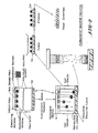
- FIGURE 1 shows the standard five step process that has been previously employed in the production of printed circuit boards.
- Each one of the circuit boards produced has routinely required the application of a dry film to a conductive substrate, such as copper, that is laminated to a nonconductive substrate, such as fiberglass epoxy, with pressure and heat.
- a mask is then applied over the dry film to permit selective exposure from a light source or other source of actinic radiation to produce the desired pattern.
- Development takes place by removing the uncross-linked dry film, leaving only cross-linked dry film with the desired pattern.
- Etching with an acid etchant removes the conductive copper substrate from between the areas of cross-linked dry film.
- stripping the dry film from the remaining conductive copper substrate exposes the desired circuit pattern. This is commonly known as the print and etch process.
- a permanent master is produced with the use of a photosensitive material or coating, such as a dry film or liquid photoresist over a conductive substrate. Thereafter, dry film or liquid photoresist is not employed to produce the desired conductive wiring patterns from the permanent master on the product circuit boards.
- the permanent master is used as an electrostatically imageable surface as shown in FIGURE 2.
- a conductive backing has a photosensitive material, such as a dry film or liquid photoresist, applied to it on at least one side. This photosensitive material undergoes a change in resistivity upon exposure to actinic radiation because of the cross-linking of the polymers in the material.
- a persistent image is formed on the photosensitive material by actinicly radiating through a mask or by "writing" the desired pattern with a digital laser pen. Either method produces electrostatic contrasts or differences in the resistivity between imaged and non-imaged areas on the photosensitive material.
- the electrostatically imageable surface is isolated from ground and charged with a corona charging device to produce the charged latent image.
- the electrostatically imageable surface is then developed by the application, through surface adsorption, of a liquid comprised at least partially of a nonpolar insulating solvent that serves as a liquid carrier to toner particles that are charged oppositely to the charge of the electrostatically imageable surface.
- This application can be accomplished by flooding, dipping or spraying the electrostatically imageable surface.
- the charged toner particles are directed to the latent image area of the electrostatically imageable surface to form or develop the latent image.
- the image is formed on the electrostatically imageable surface according to the persistent latent image's pattern on the permanent master.
- the developed image thus is ready for transfer to an electrically isolated conductive receiving surface to produce a circuit board with the desired conductive wiring pattern.
- the conductive receiving surface is first coated with a liquid that comprises at least partially a nonpolar insulating solvent.
- the solvent is the same as or an equivalent to that which is applied to the electrostatically imageable surface and may be applied by sponge, squeegee, rubber roller or other means capable of applying a thin continuous film.
- the solvent should preferably have a high resistivity and a low viscosity to permit the charged toner particles to migrate or flow through the solvent from the charged electrostatic latent image area on the electrostatically imageable surface to the conductive receiving surface.
- the solvents are generally mixtures of C9-C11 or C9-C12 branched aliphatic hydrocarbons sold under the tradename Isopar G and Isopar H, respectively, manufactured by the Exxon Corporation, or equivalents thereof.
- the electrical resistivity is preferably on the order of at least about 109 ohm-centimeters and the dielectric constant preferably is less than about 3 1/2. The use of nonpolar insulating solvents with these characteristics helps to ensure that the pattern of charged toner particles is not dissipated.
- the voltage necessary to establish the electric field between the electrostatically imageable surface and the conductive receiving surface operably can be between about 200 to about 3500 volts, but is preferably between about 200 and about 1500 volts and optimally is as stated above.
- the ability to transfer a high resolution image is a function of the combined factors of the toner, the liquid carrier, the gap spacing and the voltage applied. Generally, a greater gap spacing requires a higher voltage to effect a high quality, high resolution image transfer.
- a uniform spacing across this gap is maintained by the use of spacer strips or gap spacers, seen in FIGURE 2, which are electrically isolated from ground.
- the developed image from the electrostatically imageable surface is transferred across the gap through the liquid medium to the conductive surface to form an imaged area in a pattern similar to that of the phototool where the transferred toner particles are present and non-imaged areas where the particles are absent.
- the transfer of the developed image across the liquid-filled gap takes place at the point of transfer by maintaining a first plane taken through the electrostatically imageable surface parallel to a second plane taken through the conductive receiving surface.
- the electrostatically imageable surface and the conductive receiving surface at the point of transfer should have no relative motion occuring between them, although the point of transfer could be a stationary or rolling point of transfer.
- a drum or web, or a stationary flat surface could be employed for the electrostatically imageable surface, transferring the developed image across the gap to a flat and stationary, or a moving conductive receiving surface.
- the moving conductive receiving surface could be a rolling drum or a web or other appropriate means.
- the electrostatically imageable and conductive receiving surfaces must be held in place at the point of transfer, such as by a vacuum, or alternatively could be accomplished by magnetically or electrostatically holding the surfaces in place across the gap.
- This gap between the electrostatically imageable surface and the conductive receiving surface is preferably maintained between at least about 3 mils (.003 inch) and about 10 mils (.010 inch) by the use of spacer strips of the desired thickness, although high quality images have been transferred across gaps as large as about 20 mils (.02 inch).
- the gap greater than about 3 mils, the inconsistencies or irregularities in the two surfaces are separated sufficiently to prevent any contact from occurring between the two surfaces and any possible abrasion or scratching from occuring to the surface of the master or electrostatically imageable surface.
- the spacer strips or gap spacers are selected from either conductive materials, such as metal, or nonconductive materials, such as polyester film sold under the tradename MYLAR, or cellophane.
- the strips must be electrically isolated from ground and be of uniform thickness. The uniform thickness insures that a uniform gap spacing is obtained between the electrostatically imageable surface and the conductive receiving surface.
- the spacer strips preferably should be placed outside of the image area.
- the first and second layers of nonpolar insulating solvent By applying the first and second layers of nonpolar insulating solvent in sufficient thickness to the electrostatically imageable surface and the conductive receiving surface to fill the gap therebetween, the first liquid surface and the second liquid surface of the first and second layers of the nonpolar insulating solvent join together to form a continuous liquid transfer medium at the point of transfer of the charged toner particles between the electrostatically imageable surface and the conductive receiving surface.
- the charged toner particles are directed through the liquid transfer medium formed by the joining of the two layers of nonpolar insulating solvent at this point of transfer by the electric field that is applied at the point of transfer.
- the charged toner particles with their predetermined charge migrate from the oppositely charged cross-linked imaged area with the photosensitive material on the electrostatically imageable surface to the conductive receiving surface as individual or grouped particles.
- the conductive receiving surface is laminated onto an insulating dielectric layer, such as a fiberglass epoxy.
- the applied electric transfer field causes the toner particles to migrate through the liquid transfer medium of the nonpolar insulating solvent and attach to the conductive receiving surface to create imaged areas where the toner particles are present and non-imaged areas where they are absent.
- the photosensitive material such as a dry film or liquid photoresist
- the electrostatically imageable surface acts as a master electrostatic image plate
- the resistivity difference between the imaged and non-imaged areas on the electrostatically imageable surface remains relatively constant in most instances for sustained periods of time dependent upon the photoresist used
- multiple copies can be made by the electrostatic transfer method.
- excess nonpolar insulating solvent and excess toner particles on the electrostatically imageable surface should be removed, such as by rinsing, followed by a physical wiping or squeeging. Any residual electric charge on the electrostatically imageable area should be discharged, such as by charging the photosensitive material's surface with an alternating current corona.
- the desired electrostatic latent image pattern remains in the photosensitive material by using the material's ability to retain differences in resistivity for relatively long periods of time after having been exposed to actinic radiation to form cross-linked imaged areas of increased resistivity and non-imaged areas unexposed to the actinic radiation which remain the less resistive or background areas.
- the photosensitive material such as a dry film resist, typically is formed of polymers which become cross-linked to form the imaged areas of greater electrical resistivity that may be an order of magnitude more dielectric than the background or unexposed areas. Faster process speeds will require greater resistivity differentials.
- the resistivity of the photosensitive material can range between 1017 to 1011 ohm-centimeters, depending upon the material.
- the background or non-imaged areas should typically have an electrical resistivity of 1010 ohm-centimeters.
- the resistivity of various materials, including some traditionally considered as insulating materials, are known.
- Electronic grade Mylar polyester film has a resistivity of about 1017 ohm-centimeters, aluminum oxide ceramic about 1016 ohm-centimeters, various grades of mica from 1013 to 1017 ohm-centimeters, unexposed Dynachem AX dry film about 1013 ohm-centimeters, and various grades of Union Carbide's Bakelite copolymer plastics from about 107 to 1016 ohm-centimeters.
- DuPont's Riston 3615 dry film has a resistivity of about 1010 ohm-centimeters.
- imaged areas are the only areas of increased resistivity that hold a high voltage charge when charged by a D.C. charge corona, if the conductive backing is electrically grounded.
- the non-imaged or background areas with the lesser electrical resistivity very rapidly release or leak the charge through the grounded conductive backing.
- the charged toner particles suspended in the nonpolar insulating solvent are oppositely charged to these latent imaged areas so that the charged toner particles are attracted to them. This then permits the transfer of these charged toner particles from the electrostatically imageable surface across the liquid gap to the conductive receiving surface as previously described.
- the particles are fused to the conductive receiving surface by heating, as illustrated diagrammatically in FIGURE 2.
- the heat can be provided either by the use of an oven or directed warm air through an air slot so that the heat is supplied for a finite period of time sufficient to reach the temperature at which the binder or polymer forming the toner particles will solvate in the liquid which is entrained within the transferred image.
- the fusing for example, can occur for about 15 to about 20 seconds at a temperature greater than about 100°C and up to about 180°C.
- the etching step utilizes a solution that cannot remove the conductor material from the areas of the conductive receiving surface protected by the toner particles, but does attack and remove the conductor material from the areas unprotected by the toner particles.
- the particular type of etchant employed depends, in part, on the conductor material being etched and the type of resist being used, so that both acid and very mild alkaline etching solutions are possible for use. For example, when the conductive receiving surface is copper, an etchant comprising acidic cupric chloride is preferably used.
- the final step in the electrostatic transfer process to form the copy is the stripping step.
- the toner particles are appropriately removed or stripped from the imaged areas, such as by rinsing with methylene chloride, acetone, an alkaline aqueous solution or other suitable solution.
- the following examples are provided without any intent to limit the scope of the instant invention to the discussion therein.
- the examples are intended to illustrate the manner in which a permanent master with a persistent conductive latent image on the electrostatically imageable surface can be obtained and how the gap spacing and voltage levels can be varied to achieve successful electrostatic image transfer.
- the examples also illustrate, whether a photoconductor or a permanent master is used as the electrostatically imageable surface, how successful electrostatic image transfer can be achieved without the need for the application of a dry film or liquid resist to each conductive receiving surface prior to the transfer of the developed latent image from the electrostatically imageable surface.
- a liquid toner was prepared for use by preparing the following raw materials in the amounts shown in a high speed disperser:
- amphipathic graft copolymer system 606 Grams of an amphipathic graft copolymer system was prepared by mixing 104.3 grams of lauryl methacrylate and 44.7 grams of methyl methacrylate, both available from Rohm and Haas, and 3.0 grams of azobis isobutyronitrile, available from DuPont as Vazo 64.
- the monomer mixture is allowed to drip into the refluxing solvent at such a rate that it requires 3 hours for the total amount to be added.
- 0.5 grams of lauryl dimethyl amine is added and the refluxing is continued at atmospheric pressure for another hour.
- 0.1 gram hydroquinone and 3.0 grams methacrylic acid are added and refluxing continued under a nitrogen blanket until about 52 percent esterification of the glycidyl groups is effected (about 16 hours).
- the resulting product is slightly viscous straw-colored liquid.
- liquid toner concentrate was prepared by combining the following in a static attritor-type mill:
- the toner concentrate was futher diluted to about 1 to about 2 percent solids to create the working solution for use in electrostatic imaging.
- a cadmium sulfide photoconductor overcoated with a MYLAR polyester film layer (typical of the NP process type) was corona charged and then light exposed to a circuit trace pattern from about 0.75 to about 2.70 microjoules/square centimeter in a Canon Model 1824 copier to create a charged latent image.
- the charged latent image was developed by applying the liquid toner to the overcoated cadmium sulfide photoconductor that is the electro- statically imageable surface.
- the electrostatically imageable surface of this photoconductor is mounted over an inner aluminum substrate drum. The drum was removed from the copier.
- a high voltage power source had its ground lead connected to the interior of the drum and its positive lead connected to the copper surface of the conductive receiving surface.
- Cellophane spacer strips or gap spacers were used between the drum and the conductive surface.
- the conductive surface was coated with a liquid that included the nonpolar insulating solvent that was squeegeed onto the conductive surface.
- the electrostatically imageable surface of the drum was coated during the development step. 1000 Volts D.C. current was applied and the gap was set at 10 mils.
- the cadmium sulfide drum was manually rolled across the spacer strips to create points of transfer of the latent image from the electrostatically imageable surface to the conductive receiving surface of copper.
- the image transfer was successful with the image possessing excellent resolution and good density.
- Example 1 The cadmium sulfide photoconductor drum of Example 1 was cleaned and dried and reimaged as in Example 1.
- the liquid transfer medium was applied to the conductive receiving surface. 500 Volts of D.C. voltage was applied and the same gap space was set as in Example 1.
- the image transfer was successful, but the amount of the transferred toner particles forming the transferred image was less than the amount in Example 1 and was very light over the entire image area. There appeared to be insufficient voltage applied to transfer the majority of the toner particles over a 10 mil gap.
- Example 2 The same steps and liquid transfer medium as employed in Example 2 were repeated.
- the conductive receiving surface was wetted with the liquid transfer medium by applying to the conductive receiving surface with a squeegee.
- the spacer strips were set at 3 mils to achieve a uniform 3 mil separation between the two surfaces and a voltage of 1000 volts was employed.
- Example 3 The same steps and liquid transfer medium were employed as in Example 3, but the gap spacers were 3 mil thickness to establish the 3 mil gap between the electrostatically imageable surface and the conductive receiving surface. 200 Volts D.C. current was applied to establish the electric field. A very clear high resolution image was transferred from the electrostatically imageable surface to the conductive receiving surface, which exhibited good reflectance image density. The density of the pad areas and line traces, however, was somewhat less than that achieved in Example 3 because all of the toner particles apparently were not transferred.
- Example 2 The same steps and liquid transfer medium were employed as used in Example 2, but the liquid was squeegeed on.
- the gap spacers were 1 mil thick to establish a 1 mil gap between the electrostatically imageable surface and the conductive receiving surface. 1000 Volts D.C. was applied to create the electric field.
- the transferred image had good image density, but there were many hollow spots due to arcing. Some image distortion was present, apparently due to the closeness of the two surfaces and the resultant "squishing" of the toner particles.
- the use of a system, such as a vacuum hold-down system, which permits the receiving substrate to be held rigidly flat would have reduced the image distortion. Most of the transferred image was not distorted.
- a 4" x 5" electrically conductive substrate of copper mounted on a glass epoxy support substrate known as FR 4 was selected as the conductive substrate for use in making the electrostatically imageable surface of the permanent master.
- the copper substrate was checked for need of cleaning or degreasing. If necessary, the substrate can be cleaned with methyl chloride, methylene chloride or trichloroethylene to promote good adhesion of the photoresist to the cleaned surface during the subsequent lamination step. In this particular instance cleaning was not necessary.
- DuPont Riston 215 dry film photoresist was laminated to the substrate as the photosensitive material. The lamination was accomplished with the use of a Western Magnum Model XRL-360 laminator made by Dynachem of Tustin, CA.
- the lamination was carried out at a roll temperature of about 220°F and a speed of about six feet per minute.
- a protective top layer of approximately .001 inch thick polyethylene terephthalate, hereafter PET, film was retained over the dry film photoresist of the copper/Riston 215 laminate.
- the laminate was exposed to actinic radiation through a negative phototool using the Optic Beam 5050 exposure unit manufactured by Optical Radiation Corporation. The exposure was accomplished after the laminate cooled to room temperature following the laminating process. The exposure level was approximately 250 millijoules for about 60 seconds.
- the phototool was a Microcopy Test Target T-10 resolution test chart, with groups of bars varying from 1.0 cycles or line pairs per millimeter to 18 cycles or line pairs per millimeter, sold by Photographic Sciences, Inc.
- the exposed electrostatically imageable surface was then allowed to cool to room temperature for about 30 minutes, thereby permitting cross-linking in the dry film to complete.
- the protective layer of PET film was peeled away.
- the copper substrate was grounded and the electrostatically imageable surface was corona charged so that the imaged area received a positive charge.
- the charged persistent image was then electrophotographically developed with liquid toner of Example 1. Excess toner particles were rinsed from the developed permanent master with Isopar H solvent carrier without allowing the toner to dry.
- the developed persistent image on the electrostatic master was then ready for transfer to a conductive receiving surface.
- the electrostatic master thus formed was laid flat on a generally flat working surface.
- MYLAR® polyester spacer strips were placed along a pair of parallel and opposing edges of the master outside of the developed image area to a thickness of about 10 mils.
- a flexible conductive receiving surface of 1/2 ounce copper foil laminated to a 1 mil thick Kapton® polyimide insulating layer was wrapped around and secured by lap taping the edges to a 1 1/2 inch diameter drum.
- the receiving surface was wet with a layer of Isopar H solvent carrier by immersing the cylinder. Alternatively, the receiving surface could be coated by pouring the liquid thereover.
- An electrical potential of about 1000 volts was established to create an electric field across an approximately 10 mil gap.
- the conductive receiving surface of copper foil was charged with positive polarity with respect to the electrically conductive copper substrate of the master for use with the negatively charged toner particles.
- the 1 1/2 inch diameter drum with the conductive receiving surface secured thereto was rolled over the spacer strips on the edges of the master. As the roller passed over the master at each discrete point of transfer the toner particles were transferred from the master to the conductive receiving surface.
- the transferred image displayed excellent resolution up to about 3.6 line pairs per millimeter. It appeared as though 100% of the toner particles were transferred to the conductive receiving surface.
- the conductive receiving surface was then exposed to a fan for up to about 30 seconds to dry the non-imaged areas that comprise the background areas.
- the non-imaged areas should be dried while the imaged areas remain wet so the polymers in the toner particles can solvate in the solvent carrier and not run outside of the imaged areas.
- An air knife can also be used to effect the drying of the non-imaged areas.
- the transferred image on the conductive receiving surface was then fused by placing in an oven for about 30 seconds.
- the temperature of the oven prior to opening was about 180°C.
- the fusing is accomplished through a temperature ramping that effectively occurs when the oven door is opened to place the conductive receiving surface inside because of the resultant temperature drop within the oven.
- the oven temperature gradually increases to the approximate 180°C temperature level after the oven door is closed again.
- Example 6 The permanent master of Example 6 was cleaned and dried. The same liquid toner and the same charging technique were employed to electrophotographically develop the charged persistent image as in Example 6.
- the developed electrostatic master was laid on a generally flat working surface and MYLAR® polyester spacer strips were used as in Example 6 to create a thickness of about 15 mils.
- a flexible copper foil conductive receiving surface was mounted about the 1 1/2 inch drum and wetted as described in Example 6.
- An electrical potential of about 1000 volts was established as in Example 6 to create the electric field.
- the 1 1/2 inch diameter drum was rolled over the spacer strips on the edges of the master to effect the transfer of the toner particles to the conductive receiving surface.
- the transferred image displayed excellent resolution up to about 5.0 line pairs per millimeter with very slight distortion. It appeared as though about 70-80% of the toner particles were transferred to the conductive receiving surface.
- Example 6 The permanent master of Example 6 was cleaned and dried. The same liquid toner and the same charging technique were employed to electrophotographically develop the charged persistent image as in Example 6.
- the developed electrostatic master was laid on a generally flat working surface and MYLAR® polyester spacer strips were used as in Example 6 to create a thickness of about 20 mils.
- a flexible copper foil conductive receiving surface was mounted about the 1 1/2 inch drum and wetted as described in Example 6.
- An electrical potential of about 1000 volts was established as in Example 6 to create the electric field.
- the 1 1/2 inch diameter drum was rolled over the spacer strips on the edges of the master to effect the transfer of the toner particles to the conductive receiving surface.
- the transferred image displayed excellent resolution up to about 4.0 line pairs per millimeter with slight distortion. It appeared as though about 50-60% of the toner particles were transferred to the conductive receiving surface.
- Example 6 The permanent master of Example 6 was cleaned and dried. The same liquid toner and the same charging technique were employed to electrophotographically develop the charged persistent image as in Example 6.
- the developed electrostatic master was laid on a generally flat working surface and MYLAR® polyester spacer strips were used as in Example 6 to create a thickness of about 25 mils.
- a flexible copper foil conductive receiving surface was mounted about the 1 1/2 inch drum and wetted as described in Example 6.
- An electrical potential of about 1500 volts was established as in Example 6 to create the electric field.
- the 1 1/2 inch diameter drum was rolled over the spacer strips on the edges of the master to effect the transfer of the toner particles to the conductive receiving surface.
- the transferred image was distorted and inconsistent. It appeared as though about 30-40% of the toner particles were transferred to the conductive receiving surface.
- Example 6 The permanent master of Example 6 was cleaned and dried. The same liquid toner and the same charging technique were employed to electrophotographically develop the charged persistent image as in Example 6.
- the developed electrostatic master was laid on a generally flat working surface and MYLAR® polyester spacer strips were used as in Example 6 to create a thickness of about 5 mils.
- a flexible copper foil conductive receiving surface was mounted about the 1 1/2 inch drum and wetted as described in Example 6.
- An electrical potential of about 800 volts was established as in Example 6 to create the electric field.
- the 1 1/2 inch diameter drum was rolled over the spacer strips on the edges of the master to effect the transfer of the toner particles to the conductive receiving surface.
- the transferred image displayed excellent resolution up to about 5.6 line pairs per millimeter with a consistent image pattern. It appeared as though about 50% of the toner particles were transferred to the conductive receiving surface.
- the aluminum substrate was checked for need of cleaning or degreasing. If necessary, the substrate can be cleaned with methyl chloride, methylene chloride or trichloroethylene to promote good adhesion of the photoresist to the cleaned surface during the subsequent lamination step. In this particular instance cleaning was not necessary.
- DuPont Riston 215 dry film photoresist was laminated to the substrate as the photosensitive material. The lamination was accomplished with the use of a Western Magnum Model XRL-360 laminator made by Dynachem of Tustin, CA.
- the lamination was carried out at a roll temperature of about 220°F and a speed of about six feet per minute.
- a protective top layer of approximately .001 inch thick polyethylene terephthalate, hereafter PET, film was retained over the dry film photoresist of the aluminum foil/Riston 215 laminate.
- the laminate was exposed to actinic radiation through a negative phototool using the Optic Beam 5050 exposure unit manufactured by Optical Radiation Corporation. The exposure was accomplished after the laminate cooled to room temperature following the laminating process. The exposure level was approximately 250 millijoules.
- the phototool was a Microcopy Test Target T-10 resolution test chart, with groups of bars varying from 1.0 cycles or line pairs per millimeter to 18 cycles or line pairs per millimeter, and is sold by Applied Image, Inc. of Rochester, New York.
- the master thus formed was allowed to stabilize for about 30 minutes to allow photogenerated cross-linking to be completed and then the protective layer of PET film was peeled away from the dry film photoresist.
- the aluminum foil under the electrostatically imageable surface was then grounded, and the surface was corona charged so that the imaged area received a positive charge.
- the charged latent image was then electrophotographically developed by applying the liquid toner of Example 1 to the electrostatically imageable surface.
- the electrostatically imageable surface was then rinsed with Isopar H solvent carrier to remove excess toner particles.
- the permanent master was then ready for transfer of the developed image from the master to a conductive receiving surface.
- a 4" x 5" electrically conductive substrate of copper was mounted on a glass epoxy support substrate known as FR 4.
- the conductive surface of the laminate was checked to ensure that it was clean and not in need of degreasing. If necessary, the substrate can be cleaned with methyl chloride, methylene chloride or trichloroethylene to promote good adhesion of the photoresist to the cleaned surface during the subsequent lamination step. In this particular instance cleaning was not necessary.
- DuPont Riston 3615 dry film photoresist was laminated to the surface, using the Western Magnum Model XRL-360 run at a speed of six feet per minute and a roll temperature of about 220°F. A protective top layer of approximately .001 inch thick PET film was retained over the dry film photoresist of the copper/Riston 3615 laminate.
- the dry film was exposed in two steps to actinic radiation to a negative phototool.
- a pre-fogging for about five seconds by an ADDALUX Model 1421-40 unit, produced by Berkeley Technical Corporation of Woodside, NY was accomplished at an energy level of about 25 millijoules.
- the second step of the exposure process involved exposing the negative phototool and the electrostatically imageable surface to an energy level of approximately 475 millijoules or an exposure time of about 55 seconds.
- the negative phototool was a Microcopy Test Target T-10 resolution test chart sold by Applied Image, Inc. of Rochester, New York.
- the bar groups on the phototool varied the line pairs from 1.0 cycles or line pairs per millimeter to 18 line pairs per millimeter.
- the exposed electrostatically imageable surface was then allowed to cool to room temperature for about 30 minutes, thereby permitting cross-linking in the dry film to complete.
- the protective layer of PET film was peeled away.
- the copper substrate was grounded and the electrostatically imageable surface was corona charged so that the imaged area received a positive charge.
- the charged persistent image was then electrophotographically developed with liquid toner of Example 1. Excess toner particles were rinsed from the developed permanent master with Isopar H solvent carrier without allowing the toner to dry.
- the developed persistent image on the electrostatic master was then ready for transfer to a conductive receiving surface.
- the electrostatic master thus formed was laid flat on a generally flat working surface.
- Two three (03) mil thick MYLAR polyester spacer strips were placed along a pair of parallel and opposing edges of the master outside of the developed image area.
- a flexible conductive receiving surface of 1/2 ounce copper foil laminated to a 1 mil thick Kapton polyimide insulating layer was wrapped around and secured by lap taping the edges to a 1 1/2 inch diameter drum.
- the receiving surface was wet with a layer of Isopar H solvent carrier by immersing the cylinder. Alternatively, the receiving surface could be coated by pouring the liquid thereover.
- An electrical potential of about 800 volts was established to create an electric field across an approximately 3 mil gap.
- the conductive receiving surface of copper foil was charged with positive polarity with respect to the electrically conductive copper substrate of the master for use with the negatively charged toner particles.
- the 1 1/2 inch diameter drum with the conductive receiving surface secured thereto was rolled over the spacer strips on the edges of the master. As the roller passed over the master at each discrete point of transfer the toner particles were transferred from the master to the conductive receiving surface.
- the conductive receiving surface was then exposed to a fan for up to about 30 seconds to dry the non-imaged areas that comprise the background areas.
- the non-imaged areas should be dried while the imaged areas remain wet so the polymers in the toner particles can solvate in the solvent carrier and not run outside of the imaged areas.
- An air knife can also be used to effect the drying of the non-imaged areas.
- the transferred image on the conductive receiving surface was then fused by placing in an oven for about 30 seconds.
- the temperature of the oven prior to opening was about 180°C.
- the fusing is accomplished through a temperature ramping that effectively occurs when the oven door is opened to place the conductive receiving surface inside because of the resultant temperature drop within the oven.
- the oven temperature gradually increases to the approximate 180°C temperature level after the oven door is closed again.
- the electric field established between the electrostatically imageable surface and the conductive surface can be charged with either positive or negative polarity, depending upon the charge of the toner particles, to direct the charged toner particles across the liquid medium.
- Charged toner particles of negative polarity will be attracted to a positively charged conductive receiving surface or will be repelled by a negative back charging of the electrostatically imageable surface.
- charged toner of positive polarity are used, they will be attracted to a negatively charged conductive receiving surface or repelled by a positive back charging of the electrostatically imageable surface.
- the nonpolar insulating solvent can equally well be mineral spirits, as long as it possesses high resistivity and low viscosity.
- Negatively charged toner particles will be attracted to a positively charged latent image or vice versa.
- the desired image areas on the electrostatically imageable surface will be uncharged and the surrounding non-image areas will be charged the same as the toner particles to cause the charged toner particles to be repelled from the non-image areas onto the desired image area.
- the nonpolar insulating solvent can equally well be mineral spirits, as long as it possesses high resistivity and low viscosity.
- the gap spacing can equally well employ a web-to-web arrangement that will hold the electrostatically imageable surface and the conductive receiving surface at the desired distance.
- the electric field can be established in several ways. For example, with a conductive receiver surface, such as the copper laminate, or in the case of a dielectric material, such as MYLAR polyester film, backed by a conductive surface the electric field is created by direct charging. Where a dielectric receiving surface, such as MYLAR polyester film, is used front or back charging via conventional corona charging or roller charging can be employed.
- the electrostatically imageable surface can be a photoconductor, such as a cadmium sulfide surface with a MYLAR polyester film or a polystyrene or a polyethylene overcoating, a selenium photoconductor surface, or suitable organic photoconductors such as carbazole and carbazole derivative, polyvinyl carbazole and anthracene.
- a photoconductor such as a cadmium sulfide surface with a MYLAR polyester film or a polystyrene or a polyethylene overcoating
- suitable organic photoconductors such as carbazole and carbazole derivative, polyvinyl carbazole and anthracene.
- the surface can be zinc oxide, or organic photoconductors developed with toner which is fused onto the master, or a dry film or liquid photoresist.
- the type of photosensitive material applied to the conductive backing to make the permanent master may vary as long as it is permanently imageable and possesses the correct resistivity characteristics.
- the films may be aqueous, semi-aqueous or solvent based.
- Photoconductive insulating films of zinc oxide dispersed in a resin binder may also be used.
Landscapes
- Physics & Mathematics (AREA)
- General Physics & Mathematics (AREA)
- Engineering & Computer Science (AREA)
- Manufacturing & Machinery (AREA)
- Microelectronics & Electronic Packaging (AREA)
- Chemical & Material Sciences (AREA)
- Chemical Kinetics & Catalysis (AREA)
- General Chemical & Material Sciences (AREA)
- Electrostatic Charge, Transfer And Separation In Electrography (AREA)
- Manufacturing Of Printed Wiring (AREA)
- Manufacturing Of Printed Circuit Boards (AREA)
Applications Claiming Priority (4)
| Application Number | Priority Date | Filing Date | Title |
|---|---|---|---|
| US88379786A | 1986-07-09 | 1986-07-09 | |
| US883797 | 1986-07-09 | ||
| US88484786A | 1986-07-11 | 1986-07-11 | |
| US884847 | 1986-07-11 |
Publications (3)
| Publication Number | Publication Date |
|---|---|
| EP0252735A2 true EP0252735A2 (fr) | 1988-01-13 |
| EP0252735A3 EP0252735A3 (en) | 1990-04-11 |
| EP0252735B1 EP0252735B1 (fr) | 1993-06-02 |
Family
ID=27128704
Family Applications (1)
| Application Number | Title | Priority Date | Filing Date |
|---|---|---|---|
| EP19870306048 Expired - Lifetime EP0252735B1 (fr) | 1986-07-09 | 1987-07-08 | Procédé de transfert électrostatique à grande résolution d'une image à grande densité vers un substrat conducteur non poreux et non absorbant |
Country Status (3)
| Country | Link |
|---|---|
| EP (1) | EP0252735B1 (fr) |
| DE (1) | DE3786042T2 (fr) |
| HK (1) | HK62994A (fr) |
Cited By (3)
| Publication number | Priority date | Publication date | Assignee | Title |
|---|---|---|---|---|
| EP0306156A3 (fr) * | 1987-08-31 | 1989-10-04 | Olin Hunt Specialty Products, Inc. | Cylindre de transport |
| EP0523071A4 (en) * | 1990-03-26 | 1993-04-21 | Olin Corporation | A liquid color toner composition |
| US5238762A (en) * | 1990-03-26 | 1993-08-24 | Olin Corporation | Liquid colored toner compositions and their use in contact and gap electrostatic transfer processes |
Family Cites Families (5)
| Publication number | Priority date | Publication date | Assignee | Title |
|---|---|---|---|---|
| JPS4934151B1 (fr) * | 1970-06-04 | 1974-09-12 | ||
| FR2482323A1 (fr) * | 1980-05-12 | 1981-11-13 | Rhone Poulenc Syst | Procede de reproduction electrographique sur un support quelconque a l'aide d'une poudre de developpement magnetique monocomposant |
| DE3047498A1 (de) * | 1980-12-17 | 1982-07-22 | Herbert 4600 Dortmund Karnikowski | Uebertragungsfolie fuer die uebertragung von abbildungen auf oberflaechen, sowie uebertragungsverfahren und vorrichtung |
| US4411976A (en) * | 1982-01-08 | 1983-10-25 | Savin Corporation | Method of increasing the density of liquid-developed gap-transferred electrophotographic images and developing composition for use therein |
| GB8326169D0 (en) * | 1983-09-29 | 1983-11-02 | Int Research & Dev Co Ltd | Printed circuit board |
-
1987
- 1987-07-08 EP EP19870306048 patent/EP0252735B1/fr not_active Expired - Lifetime
- 1987-07-08 DE DE19873786042 patent/DE3786042T2/de not_active Expired - Fee Related
-
1994
- 1994-06-30 HK HK62994A patent/HK62994A/xx unknown
Cited By (4)
| Publication number | Priority date | Publication date | Assignee | Title |
|---|---|---|---|---|
| EP0306156A3 (fr) * | 1987-08-31 | 1989-10-04 | Olin Hunt Specialty Products, Inc. | Cylindre de transport |
| EP0523071A4 (en) * | 1990-03-26 | 1993-04-21 | Olin Corporation | A liquid color toner composition |
| US5238762A (en) * | 1990-03-26 | 1993-08-24 | Olin Corporation | Liquid colored toner compositions and their use in contact and gap electrostatic transfer processes |
| US5275906A (en) * | 1990-03-26 | 1994-01-04 | Olin Corporation | Method of forming a pattern using a liquid color toner composition |
Also Published As
| Publication number | Publication date |
|---|---|
| HK62994A (en) | 1994-07-01 |
| DE3786042T2 (de) | 1993-09-09 |
| EP0252735B1 (fr) | 1993-06-02 |
| EP0252735A3 (en) | 1990-04-11 |
| DE3786042D1 (de) | 1993-07-08 |
Similar Documents
| Publication | Publication Date | Title |
|---|---|---|
| US4786576A (en) | Method of high resolution of electrostatic transfer of a high density image to a nonporous and nonabsorbent conductive substrate | |
| US2647464A (en) | Electrography | |
| US2939787A (en) | Exposure of photochemical compositions | |
| US3656990A (en) | Electrosolography | |
| KR100714321B1 (ko) | 인쇄 배선 기판 및 플랙시블 회로의 제조 방법 | |
| US4661431A (en) | Method of imaging resist patterns of high resolution on the surface of a conductor | |
| US6815130B2 (en) | Electrostatic printing plate possessing a tiered surface | |
| US5011758A (en) | Use of a liquid electrophotographic toner with an overcoated permanent master in electrostatic transfer | |
| US4859557A (en) | Dry powder electrophotographic toner with permanent master in electrostatic transfer | |
| US2919179A (en) | Resist forming method | |
| US4717639A (en) | Process for preparation of a stencil or resist image | |
| US3196012A (en) | Half-tone xerography with thermoplastic deformation of the image | |
| US3145655A (en) | Equipotential xeroprinting member and process of printing therewith | |
| EP0252735B1 (fr) | Procédé de transfert électrostatique à grande résolution d'une image à grande densité vers un substrat conducteur non poreux et non absorbant | |
| AU603108B2 (en) | Permanent master with a persistent latent image for use in electrostatic transfer to a receiving substrate | |
| US4968570A (en) | Method of preparing a permanent master with a permanent latent image for use in electrostatic transfer | |
| AU607347B2 (en) | Method of high resolution electrostatic transfer of a high density image to a nonconductive receiving substrate | |
| JPS5743493A (en) | Method of producing printing block or printed circuit | |
| US3446616A (en) | Xerographic imaging employing a selectively removable layer | |
| US3640746A (en) | Adhesive contact electrification imaging | |
| CA1295652C (fr) | Methode electrostatique a haute definition de transfert d'images a grande densite sur un substrat conducteur non poreux et non absorbant | |
| JPS6329597A (ja) | 高濃度画像の高解像度静電転写方法 | |
| US20050100810A1 (en) | Liquid toners for electrostatic printing of functional materials | |
| JPH02288392A (ja) | 電気的に隔離された受像面上の調色されたパターンの作製方法 | |
| JPH11330672A (ja) | 回路パターン形成方法及びそれにより形成された多層配線基板 |
Legal Events
| Date | Code | Title | Description |
|---|---|---|---|
| PUAI | Public reference made under article 153(3) epc to a published international application that has entered the european phase |
Free format text: ORIGINAL CODE: 0009012 |
|
| AK | Designated contracting states |
Kind code of ref document: A2 Designated state(s): BE DE FR GB IT NL |
|
| PUAL | Search report despatched |
Free format text: ORIGINAL CODE: 0009013 |
|
| RHK1 | Main classification (correction) |
Ipc: G03G 17/04 |
|
| AK | Designated contracting states |
Kind code of ref document: A3 Designated state(s): BE DE FR GB IT NL |
|
| 17P | Request for examination filed |
Effective date: 19900817 |
|
| RAP1 | Party data changed (applicant data changed or rights of an application transferred) |
Owner name: OLIN ELECTRONIC MATERIALS, INC. |
|
| RAP1 | Party data changed (applicant data changed or rights of an application transferred) |
Owner name: OLIN HUNT SPECIALTY PRODUCTS, INC. |
|
| 17Q | First examination report despatched |
Effective date: 19920414 |
|
| GRAA | (expected) grant |
Free format text: ORIGINAL CODE: 0009210 |
|
| ITF | It: translation for a ep patent filed | ||
| AK | Designated contracting states |
Kind code of ref document: B1 Designated state(s): BE DE FR GB IT NL |
|
| PGFP | Annual fee paid to national office [announced via postgrant information from national office to epo] |
Ref country code: FR Payment date: 19930608 Year of fee payment: 7 |
|
| PGFP | Annual fee paid to national office [announced via postgrant information from national office to epo] |
Ref country code: GB Payment date: 19930621 Year of fee payment: 7 |
|
| PGFP | Annual fee paid to national office [announced via postgrant information from national office to epo] |
Ref country code: BE Payment date: 19930625 Year of fee payment: 7 |
|
| REF | Corresponds to: |
Ref document number: 3786042 Country of ref document: DE Date of ref document: 19930708 |
|
| PGFP | Annual fee paid to national office [announced via postgrant information from national office to epo] |
Ref country code: NL Payment date: 19930731 Year of fee payment: 7 |
|
| ET | Fr: translation filed | ||
| PGFP | Annual fee paid to national office [announced via postgrant information from national office to epo] |
Ref country code: DE Payment date: 19930930 Year of fee payment: 7 |
|
| RTI2 | Title (correction) |
Free format text: YETHOD OF HIGH RESOLUTION ELECTROSTATIC TRANSFER OF A HIGH DENSITY IMAGE TO A NONPOROUS AND NONABSORBENT CONDUCTIVE SUBSTRATE. |
|
| K2C1 | Correction of patent specification (title page) published |
Effective date: 19930602 |
|
| PLBE | No opposition filed within time limit |
Free format text: ORIGINAL CODE: 0009261 |
|
| STAA | Information on the status of an ep patent application or granted ep patent |
Free format text: STATUS: NO OPPOSITION FILED WITHIN TIME LIMIT |
|
| 26N | No opposition filed | ||
| PG25 | Lapsed in a contracting state [announced via postgrant information from national office to epo] |
Ref country code: GB Effective date: 19940708 |
|
| PG25 | Lapsed in a contracting state [announced via postgrant information from national office to epo] |
Ref country code: BE Effective date: 19940731 |
|
| BERE | Be: lapsed |
Owner name: OLIN HUNT SPECIALTY PRODUCTS INC. Effective date: 19940731 |
|
| PG25 | Lapsed in a contracting state [announced via postgrant information from national office to epo] |
Ref country code: NL Effective date: 19950201 |
|
| GBPC | Gb: european patent ceased through non-payment of renewal fee |
Effective date: 19940708 |
|
| NLV4 | Nl: lapsed or anulled due to non-payment of the annual fee | ||
| PG25 | Lapsed in a contracting state [announced via postgrant information from national office to epo] |
Ref country code: FR Effective date: 19950331 |
|
| PG25 | Lapsed in a contracting state [announced via postgrant information from national office to epo] |
Ref country code: DE Effective date: 19950401 |
|
| REG | Reference to a national code |
Ref country code: FR Ref legal event code: ST |
|
| PG25 | Lapsed in a contracting state [announced via postgrant information from national office to epo] |
Ref country code: IT Free format text: LAPSE BECAUSE OF NON-PAYMENT OF DUE FEES Effective date: 20050708 |