EP0253128B1 - Antenne à micro-ondes - Google Patents
Antenne à micro-ondes Download PDFInfo
- Publication number
- EP0253128B1 EP0253128B1 EP87108204A EP87108204A EP0253128B1 EP 0253128 B1 EP0253128 B1 EP 0253128B1 EP 87108204 A EP87108204 A EP 87108204A EP 87108204 A EP87108204 A EP 87108204A EP 0253128 B1 EP0253128 B1 EP 0253128B1
- Authority
- EP
- European Patent Office
- Prior art keywords
- antenna
- line
- substrate
- suspended
- feed point
- Prior art date
- Legal status (The legal status is an assumption and is not a legal conclusion. Google has not performed a legal analysis and makes no representation as to the accuracy of the status listed.)
- Expired - Lifetime
Links
Images





Classifications
-
- H—ELECTRICITY
- H01—ELECTRIC ELEMENTS
- H01Q—ANTENNAS, i.e. RADIO AERIALS
- H01Q21/00—Antenna arrays or systems
- H01Q21/06—Arrays of individually energised antenna units similarly polarised and spaced apart
-
- H—ELECTRICITY
- H01—ELECTRIC ELEMENTS
- H01Q—ANTENNAS, i.e. RADIO AERIALS
- H01Q21/00—Antenna arrays or systems
- H01Q21/06—Arrays of individually energised antenna units similarly polarised and spaced apart
- H01Q21/061—Two dimensional planar arrays
- H01Q21/064—Two dimensional planar arrays using horn or slot aerials
-
- H—ELECTRICITY
- H01—ELECTRIC ELEMENTS
- H01Q—ANTENNAS, i.e. RADIO AERIALS
- H01Q21/00—Antenna arrays or systems
- H01Q21/0006—Particular feeding systems
- H01Q21/0075—Stripline fed arrays
- H01Q21/0081—Stripline fed arrays using suspended striplines
-
- H—ELECTRICITY
- H01—ELECTRIC ELEMENTS
- H01Q—ANTENNAS, i.e. RADIO AERIALS
- H01Q21/00—Antenna arrays or systems
- H01Q21/24—Combinations of antenna units polarised in different directions for transmitting or receiving circularly and elliptically polarised waves or waves linearly polarised in any direction
Definitions
- the present invention relates to microwave antennas, and more particularly to planar antennas for receiving circularly polarized waves of a high frequency satellite broadcasting transmission.
- a number of designs have been proposed for high frequency planar antennas, particularly with respect to antennas intended to receive satellite transmissions in the 12 GHz band.
- One previous proposal is for a microstrip line feed array antenna, which has the advantage that it can be formed by etching of a substrate.
- a low loss substrate such as teflon or the like
- dielectric losses and radiation losses from this type of antenna Accordingly, it is not possible to realize high efficiency, and when a substrate is used having a low loss characteristic, the cost is relatively expensive.
- Suspended feed line antennas are illustrated in European Patent Application No. 108463-A and 123350-A, and in MSN (Microwave System News), published March 1984, pp. 110-126.
- the antenna disclosed in the first of the above applications incorporates copper foils which have to be formed perpendicularly relative to both surfaces of a dielectric sheet which serves as the substrate. Since the structure is formed over both surfaces of the substrate, the interconnection treatment becomes complicated, and the antenna is necessarily relatively large in size.
- the antenna disclosed in the other above-cited application requires copper foils to be formed on two separate dielectric sheets. It is difficult to get accurate positioning of these foils, and the construction becomes relatively complicated and expensive.
- one excitation probe is formed in each of a plurality of openings to form an antenna for a linear polarized wave. Such an antenna cannot effectively be used to receive a circular polarized wave, because the gain is poor, and two separate substrates must be used, making the construction relatively complicated and expensive.
- This antenna is in the form of a suspended line feed type planar antenna having a substrate sandwiched between a pair of metal sheets such as aluminum and metalized plastics, each of the metal sheets having a plurality of spaced openings defining radiation elements.
- a plurality of openings having a pair of excitation probes are formed perpendicularly to each other in a common plane and signals received at the pair of excitation probes are supplied to the suspended line in phase with each other.
- Fig. 1 is a plan view of a circular polarized wave radiation element used in such an antenna
- Fig. 2 is a cross-sectional view taken along a line I-I in Fig. 1.
- an insulating substrate 3 is sandwiched between first and second metal plates 1 and 2 (which may be formed of metal sheets or plates such as aluminum or metalized plastic).
- first and second metal plates 1 and 2 which may be formed of metal sheets or plates such as aluminum or metalized plastic.
- a number of openings 4 and 5 are formed in the plates 1 and 2, the opening 4 being formed as a concave depression or recess in the plate 1 and the opening 5 being formed as an aperture in the plate 2.
- a pair of excitation probes 8 and 9, oriented perpendicular to each other, are formed on the substrate 3 in a common plane, in alignment with the openings 4 and 5 as illustrated in Fig. 1.
- the excitation probes 8 and 9 are each connected with a suspended line conductor 7 located within a cavity portion 6 which forms a coaxial line for conducting energy between the excitation probes 8 and 9 and a remote point.
- the substrate 3 is in the form of a thin flexible film sandwiched between the first and second metal or metalized plates 1 and 2.
- the openings 4 and 5 are circular, and of the same diameter, and the upper opening 5 is formed with a conical shape as illustrated in Fig. 2.
- the suspended line conductor 7 comprises a conductive foil supported on the substrate 3 centrally in the cavity portion 6 to form a suspended coaxial feed line.
- Fig. 3 is a cross-sectional view taken along a line II-II in Fig. 2. As illustrated in Fig. 3, the conductive foil 7 forms the central conductor and the conductive surface of the plates 1 and 2 form the outer coaxial conductor.
- the foil 7 is formed as a printed circuit by etching a conductive surface on the substrate 3, so as to remove all portions of the conductive surface except for the conductive portions desired to remain such as the foil 7, and the excitation probes 8 and 9, etc.
- the conductive foil has a thickness of, for example, 25 to 100 micrometers. Since the substrate 3 is thin and serves only as a support member for the foil 7, even though it is not made of low loss material, the transmission loss in the coaxial line is small.
- the typical transmission loss of an open strip line using a teflon-glass substrate is 4 to 6dB/m at 12 GHz, whereas the suspended line has a transmission loss of only 2.5 to 3 dB/m, using a substrate of 25 micrometers in thickness. Since the flexible substrate 3 is inexpensive, as compared with the teflon-glass substrate, this arrangement is much more economical.
- t designates the thickness of the substrate 3
- L the width of the cavity portion 6,
- d the height of the cavity portion 6
- W the width of the suspended line conductor 7.
- Fig. 5 illustrates that the conductive foil 7 is formed into elongate feed lines, arranged perpendicular to each other, where they are connected to the excitation probes 8 and 9, and connected together by a common leg.
- the foils are connected to a feed line at the point 11, which is offset relative to the center of the common leg, as shown in Fig. 5, so that the excitation probe 9 is fed by a line having a longer length, indicated by reference numeral 10, of one quarter of wavelength, relative to the length of the feed in the excitation probe 8.
- the wavelength referred to here is the wavelength of energy within the waveguide or suspended line 7, indicated by ⁇ g/4, which wavelength is determinable from the frequency of the energy and the geometry of the waveguide.
- the phase of the signal applied to the excitation probe 8 (as a transmitting antenna) is advanced by a quarter of the wavelength (relative to the center frequency of the transmission band) compared with that applied to the excitation probe 9.
- This arrangement when used as a receiving antenna, allows a clockwise circular polarized wave to be received, since the excitation probe 8 comes into alignment with the rotating E and H vectors of the wave one quarter cycle after the excitation probe 9 is in such alignment. Because of the increased length 10 of the foil line connected with the excitation probe 9, the excitation probes 8 and 9 contribute nearly equal in-phase components to a composite signal at the T or combining point 11.
- Fig. 6 illustrates a circuit arrangement in which a plurality of radiation elements, each like that illustrated in Figs. 1-5 are interconnected by foil lines printed on the sheet 3.
- Each of the radiation elements contributes a signal in phase with the signal contributed by every other radiation element, which are interconnected together at a feed point 12. It will be apprehended from an examination of Fig. 6 that the length of the foil line 7 from the point 12 to any of the individual excitation probes 8 and 9, constitutes an equal distance, so that the signals received from each radiation element arrive at the feed point 12 in phase with the others.
- the array of Fig. 6 shows the printed surface on the substrate 3, and the aligned position of the openings 4 in the plate 2.
- the substrate 3 is sandwiched between the conductive plates 1 and 2 having the openings 4 and 5 (Fig. 2) aligned with each of the radiation elements, so that all of them function in the manner described above in connection with Figs. 1 to 5.
- Fig. 6 Using the general arrangement illustrated in Fig. 6, it is possible to obtain various radiation patterns, by changing characteristics of the lines. For example, if the distance from the common feed point 12 to the excitation probes 8 and 9 of some of the radiation elements is changed, the phase of the power contributed by those radiation elements can be changed. Further, if the ratio of impedance is changed by reducing, or increasing the thickness of the suspended lines at the places where it is branched (as shown in Fig. 5), it is possible to change the amplitude of the signals contributed from the branches to the common line of the branch. This affects the relative power and phase of the signals contributed from each of the receiving elements, with the result of changing the radiation pattern of the antenna.
- Fig. 7 is a cross-sectional view taken along a line III-III in Fig. 6.
- a dashed line in Fig. 7 illustrates that the circuit in Fig. 6 is covered with the second metal plate 2. It will be apphrehended from Fig. 7 that the cavity portions 6 are made in alignment with individual conductor foils 7.
- the spacing between horizontally-adjacent radiation elements must be selected in the range from 0.9 to 0.95 wavelength relative to 12 GHz wave in free space (ranging from 22.5 to 23.6 mm) in order to obtain high gain (high efficiency).
- This causes the width of the groove of the suspended line interconnected through the radiation elements, or the width of the cavity portion 6 to be limited under about 2 mm, thus putting a limitation on decreasing the transmission loss.
- the freedom in designing the antenna is restricted.
- the groove (cavity portion) having a narrow width must be formed on the whole of the array surface along the conductive foil, so that the manufacturing process is complicated and that strict accuracy is required because the groove must be sandwiched by the metal plates 1 and 2.
- the accuracy of the dimension required for removal of metal and for forming the metalized plastic plate is difficult to assure particularly for the mass-production. This problem becomes serious for the groove portion of the suspended line.
- the antenna can be made very thin, and with a simple mechanical arrangement. Even when inexpensive substrates are used, the gain obtained from the antenna is equal to or greater than that of an antenna which uses the relatively expensive microstrip line substrate technology.
- the width of the cavity portion for the suspended line is selected as 1.75 mm, and the diameter of the radiation element or the openings 4 and 5 formed in the plates 1 and 2 is selected as 16.35 mm.
- the line width is selected to be wider than 2 mm, and a reduced diameter of the radiation element. For example, for most effective reception, the diameter must be reduced from 16.35 to about 15.6 mm.
- the cut-off frequency of the dominant mode (TE11 mode) of the circular waveguide having this diameter becomes about 11.263 GHz.
- the characteristics of the return losses change, with the result that the return loss near the operation frequency (11.7 to 12.7 GHz) deteriorates.
- the "return loss” refers to the loss resulting from reflection due to unmatched impedances.
- the loss caused by the feed line is a main factor which determines the antenna gain (operation gain). This becomes serious, particularly when a gain of 30dB or more is obtained.
- the afore-mentioned problems can be solved to some extent.
- the feed circuit network for receiving a circular polarized wave is supplied with a power and phase as mentioned before, if the spacing between the adjacent radiation elements is selected in a range from 0.9 to 0.95 wavelength in order to obtain the maximum gain, the width of the groove constructing the suspended line is about 2 mm for 12 GHz wave band.
- the transmission loss is large.
- the line width is selected to be constant and narrow, so that the feed loss (transmission loss) cannot be minimized. Further, even though the diameter of the radiation element is reduced and the width of the feed line is increased as much as possible under the condition that the spacing between the radiation elements is made constant, there still remains a limit on minimizing the transmission loss.
- a satellite broadcasting reception system generally comprises a reception antenna located outdoors, a low noise converter, a connection cable and a receiver located indoors, electrically connected through the connection cable to thereby receive a television picture and sound.
- a parabolic antenna is normally employed as a reception antenna and includes a primary radiator located at the focus point to derive radio waves collected by a reflection mirror and a succeeding converter of low noise.
- the assignee of the present invention has previously proposed a planar array antenna to receive a satellite broadcasting (see U.S. Patent Application Serial No. 888,117).
- excitation probes are provided on a substrate in a common plane, in alignment with the number of openings, with each forming one portion of a radiation element, and one radiation element near the probe of the central portion is removed and replaced by a feed point, whereby the transmission loss of the feed line is reduced and the antenna is simplified in construction and becomes high in gain and more economical.
- the apparatus When an antenna like a parabolic antenna is used to receive a satellite broadcasting, the apparatus is located in three-dimensional space, so that the mounting of the antenna becomes difficult and that a large space is required. In addition, since a primary radiator and a converter of low noise type are both located in the curved surface within the space, the performance of the antenna is affected by the snowfall or the like and thereby deteriorated in efficiency.
- a suspended line feed type planar array antenna according to the preamble of Claim 1 is known from the document EP-A1-0 108 463.
- the antenna of the invention is characterized in that said holding portions are annular and are disposed around each of said openings, and said plates are recessed to provide a cavity surrounding said holding portions.
- Fig. 8 illustrates an embodiment of the present invention in which a plurality of circular polarized wave radiation elements (Figs. 1 to 5) are powered all in phase, from a feed point 12.
- Fig. 9 is a cross-sectional view taken along a line VI-VI in Fig. 8.
- a dashed line in Fig. 9 illustrates that the second metal plate 2 is put on the array of Fig. 8 during assembly.
- a holding portion 13 to hold the substrate 3.
- a holding portion 13a to hold the substrate 3.
- a holding portion 13b is formed over the outer peripheral portion of the array.
- Other remaining portions are formed to have a depth equal to, for example, that of the cavity portion 6 shown in Fig. 2 to thereby form a groove, or cavity portion 14 on the metal plate 1 as shown in Fig. 9.
- the area 15 need not be decreased in thickness to form a cavity portion, but be left as a holding portion.
- the feed portion 12 need not have therearound the special holding portion 13a and the area 15 serves as the holding portion. If the feed portion 12 is provided at the portion at which a central radiation element is removed in order to reduce the transmission loss by reducing the length of the feed line (see U.S. Patent Application Serial No. 888,117), the special holding portion 13a is provided around the feed portion 12 as illustrated in Fig. 8.
- the holding portions and the cavity portions are formed on the second metal plate 2 in alignment with those of the first metal plate 1. Though not shown, the holding portions are formed around each of the openings 5 bored through the second metal plate 2, around the feed portion (its upper surface is closed) and around the outer peripheral portion of the antenna array. Other portions are formed to have a concave depression or recess so as to form the cavity portions.
- the substrate 3 Since the substrate 3 is uniformly held by the holding portions 13, 13a and 13b, the substrate 3 is prevented from being deformed.
- the first and second metal plates 1 and 2 closely sandwich the perimeters of the radiation elements, the feed portion and so on, avoiding the occurrence of resonance at a specific frequency.
- a plurality of knock pins are formed on one of the first and second metal plates 1 and 2 at their portions through which the suspended lines are not passed and through-holes are formed through the substrate 3 and the other metal plate to receive with the above mentioned knock pins. Therefore, the positioning of the metal plates 1 and 2 and the substrate 3 can be made with each by engaging the knock pins into the through-holes.
- the planar array antenna since the common cavity portion is substantially formed by removing the partition wall of the cavity portion at every line in the prior art, the planar array antenna does not require so high an accuracy, it can be manufactured with ease by machinery. Further, the freedom in designing the suspended line is increased and the transmission loss is reduced, with the result that the gain (or efficiency) of the antenna can be increased.
- the holding portions are formed around a great number of openings, each forming a portion of the radiation element, and since the cavity portion is provided at least between the adjacent openings as a groove portion, the suspended line is not from being restricted by the cavity portion, so that the array antenna can be mechanically processed and molded with ease and the accuracy of the dimension thereof can be relieved.
- the transmission loss of the line is decreased, with the result that the antenna gain (or efficiency) can be increased.
- the planar array antenna can be improved by a single thin film-shaped substrate and can receive circularly polarized waves.
- the substrate of a thin film is substantially held by the holding portions formed around the circular radiation elements, the suspended line can be constructed uniformly.
- the perimeters of the circular radiation element and the feed portions are closely sandwiched between the upper and lower metal plates, the occurrence of the resonance or the like at a specific frequency can be avoided.
- Figs. 10 and 11 illustrate the arrangement of the circular polarized wave radiation element used in this embodiment.
- Fig. 10 is a plan view and
- Fig. 11 is a cross-sectional view taken along a line V-V in Fig. 10.
- like parts corresponding to those of Figs. 1 and 2 are marked with the same references and therefore need not be described in detail.
- the insulating substrate 3 is sandwiched between the metal plates 1 and 2 (which may be formed of sheet metal such as aluminum or metalized plastic).
- a number of openings 4 and 5 are formed in the plates 1 and 2, the opening 4 being formed as a concave depression or recess in the plate 1 and the opening 5 being formed as an aperture in the plate 2.
- a pair of excitation probes 8 and 9, oriented perpendicular to each other, are formed on the substrate 3 in a common plane, in alignment with the openings 4 and 5 as illustrated in Fig. 10.
- the excitation probes 8 and 9 are each connected with the suspended line conductor 7 located within the cavity portion 6 which forms a coaxial line for conducting energy between the excitation probes 8 and 9 and a remote point.
- the substrate 3 is in the form of a thin flexible film sandwiched between the first and second metal or metalized plates 1 and 2.
- the openings 4 and 5 are circular, and of the same diameter, and the upper opening 5 is formed with a conical shape as illustrated in Fig. 11.
- the suspended line conductor 7 comprises a conductive foil supported on the substrate 3 centrally in the cavity portion 6 to form a suspended coaxial feed line.
- the conductive foil 7 forms the central conductor and the conductive surface of the plates 1 and 2 form the outer coaxial conductor.
- conductive metal segments 22 and 23 are aligned with the excitation probes 8 and 9 within each radiation element. These elements 22 and 23, as shown in Figs. 10 and 11, are aligned end to end and in line with the excitation probes 8 and 9 and spaced apart therefrom.
- the conductive segments 22 and 23 are elongate, rectangular and are formed as printed circuits or otherwise deposited on the surface of the substrate 3. They extend beyond the perimeter of the opening 5 to be in electrical contact at one ends thereof with the metal plate 2.
- the use of the conductive segments 22 and 23 makes it possible to lower the cut-off frequency of the radiation element, and to improve the return loss, or VSWR (voltage standing wave ratio) of the conversion (excitation) probe from the suspended line to the waveguide mode.
- the isolation between the coupling probes 8 and 9 is greater than 20 dB, so the radiation element effectively receives (transmits) a circular polarized radiation in the same manner as described above.
- the cut-off frequency is lowered, so that the matching can be established to improve the return loss.
- the diameter of the openings 4 and 5 of the radiation element is selected as 15.6 mm, then a waveguide having a small diameter can be used, and the image suppression is improved.
- Fig. 12 is a diagram showing a practical circuit arrangement for combining circular polarized waves.
- a pair of excitation probes 8 and 9 are connected by the suspended line conductive foils 7 in a common plane on the substrate 3.
- a line 10 of ⁇ g/4 (where ⁇ g is a line wavelength at the center frequency) corresponding to ⁇ /4 is connected to one of the foils 7 which is advanced in phase so that the waves becomes equal in phase at a composing section 11.
- This arrangement when used as a receiving antenna, allows a clockwise circular polarized wave to be received, since the excitation probe 8 comes into alignment with the rotating E and H vectors of the wave one quarter cycle after the excitation probe 9 is in such alignment. Because of the increased length 10 of the foil line connected with the excitation probe 9, the excitation probes 8 and 9 contribute nearly equal-in phase components to a composite signal at the T or combining point 11.
- an array is illustrated in which a plurality of circular polarized wave radiation elements shown in Fig. 10 or 13 are powered through the suspended lines all in phase, from a common feed point 24.
- the array is formed of 256 (16 x 16) circular polarized wave radiation elements. This array forms a square of 40 cm by 40 cm.
- a plurality of openings 4 and 5 are formed through the first and second metal plates 1 and 2 in alignment with the circular polarized wave radiation elements, respectively.
- the excitation probes 8 and 9 of the respective radiation elements are interconnected to the common feed point 24 via the suspended line conductive foils 7, in such a fashion that the lengths of the interconnecting lines are all equal in length.
- the phase of the power contributed by these radiation elements can be changed.
- the ratio of impedance is changed by reducing, or increasing the width of the suspended lines at the places where it is branched, it is possible to change the amplitude of the signals contributed from the branches to the common line of the branch and to thereby vary the directivity of the antenna.
- Fig. 13 shows, one of the radiation elements closest to the center of the array is removed, and a feed waveguide converter, the outline of which is shown in rectangular dashed box 25, is attached to the array at this point.
- a waveguide (not shown) is connected through this waveguide converter 25 to the common feed point 24.
- the transition from a rectangular waveguide to the coaxial line is made in the conventional way and therefore need not be described in detail.
- a resistor 26 is provided to terminate the line normally connected to the removed radiation element with the characteristic impedance of the feed line, to avoid any reflection effect by the removal of this radiation element.
- the width of the suspended lines where they are provided independently is increased as shown by reference numerals 7'. That is, the suspended line is formed of the cavity portion 6 and the conductive foil 7, so that if the suspended line is independently provided between the radiation elements, the width of the suspended line is increased. Referring to Fig. 13, the suspended line conductive foil 7' is independently provided between the radiation elements and the width thereof is made larger than that of other suspended lines 7. Of course, the width of the cavity portion 6 where the suspended line passes therethrough is increased accordingly, though not shown.
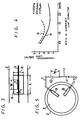
- t designates the thickness of the substrate 3
- L the width of the cavity portion 6,
- d the height of the cavity portion 6
- W the width of the suspended line conductor 7.
- t 25 micrometer
- d 1.4 mm
- L 2 mm
- W 1 mm in practice.
- the transmission loss is about 3 dB/m as shown by a dashed curve a in Figs. 4.
- the transmission loss becomes about 1.8 dB/m as shown by solid curve b in Fig. 4. Accordingly, if the length of the portion in which the width of the suspended line conductor 7 can be increased is 50 cm, it becomes possible to increase the antenna gain by about 0.6 dB/m as compared with the prior art.
- the present invention is applied to the circular polarized wave planar array antenna as described above, the present invention is not limited to the circular polarized wave planar array antenna, but can be similarly applied to other planar antennas. Further, the present invention is not limited to the planar array antenna of the suspended line configuration but can be similarly applied to the planar antenna of the microstrip line configuration.
- the line width of the feed line such as the suspended line is increased in part, the loss of the feed line, or the transmission loss can be reduced and the antenna gain can be improved.
- Fig. 14 illustrates another embodiment of the film-shaped substrate 3 of the planar array antenna according to the present invention.
- like parts corresponding to those of Fig. 13 are marked with the same references and will not be described in detail.
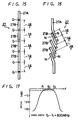
- a filter 27 is provided just before the common feed point 24.
- the length of a gap G between adjacent island-shaped portions 27B is selected to be narrower at the end portion and wider at the central portion (for example 0.1 mm at the edge portion and 1 mm at the central portion).
- the filter 27 is formed of five island-shaped portions 27B but the filter 27 may be formed of two or three or more than 5 island-shaped portions 27B.
- Such a filter is called an end-coupled type filter and it is disclosed in Microwave Journal, July 1986, pp. 75-84.
- the respective island-shaped portions 27B may be each located with an inclination of, for example, about 45°.
- notch portions N may be formed on the island-shaped portions 27B of both ends in order to effect the impedance matching.
- This type of filter is called a parallel-coupled type filter and it is disclosed in Microwave Journal, October 1980, pp. 67-71.
- the filter 27 shown in Figs. 15 and 16 is designed as a bandpass filter with a bandpass characteristic having a band width, f1 - f2 of 800 MHz around a desired frequency f0 (ranging from 11.7 to 12.7 GHz) as shown in Fig. 17.
- the use of this filter 27 makes it possible to cut off undesired frequency components and to avoid various disturbances such as image interference and the like.
- the filter 27 is formed with other elements at the same time on the common film-shaped substrate by using the conductive foils so that the arrangement of the filter 27 can be simplified considerably.
- the filter 27 can be formed together with the circuit arrangement shown in Fig. 6.
- Figs. 18 and 19 illustrate an embodiment of the waveguide converter used in the above embodiments of the present invention.
- Fig. 18 is a plan view of such waveguide converter and
- Fig. 19 is its rear view (showing the rear surface to which the antenna is attached).
- a converter main body 31 which has formed on its upper portion an input portion 32 so as to be connected to the planar array antenna (not shown).
- the input portion 32 is of a waveguide structure and has therearound a flange 33 used to attach the converter to the antenna.
- Tapped holes 34 are formed through the flange 33 at its four corners. Since one of these tapped holes 34a at the position nearest the converter main body 31 does not receive a screw, it is made in the form of, for example, a hemisherical-shaped convexity for positioning.
- a conversion probe 35 interconnected with the internal circuit in the converter 31 is projected into the inside of the input portion 32 as shown in Fig. 19.
- the converter main body 31 is fixed to the planar array antenna (not shown) by a belt 36 which has a pair of tapped holes 37 formed therethrough at its both ends.
- the converter main body 31 has an output connector 38 to which a coaxial cable (not shown) is connected.
- Fig. 20 is a rear view of the planar array antenna (as seen from the rear surface to which the waveguide converter is attached) and Fig. 21 is a side view illustrating that the waveguide converter is attached to the planar array and antenna of this invention.
- the planar array antenna comprises first and second metal plates (or metalized plastic plates) 1 and 2 and a thin film-shaped substrate (film-shaped flexible substrate) 3 sandwiched between the first and second metal plates 1 and 2.
- the first metal plate 1 has formed thereon a plurality of openings 4, each of which takes the form of concavity or concave depression.
- the second metal plate 2 has formed thereon a plurality of openings 5 of the same diameter as that of the opening 4 and each of which is formed as a concial shaped opening at its upper portion. Then, the openings 4 and 5 are communicated with each other.
- the openings 4 and 5 coincide with each other in axial alignment when positioned accurately.
- the feed portion 24 is provided on the antenna at its place where one centrally located radiation element is removed. This feed portion 24 protrudes to the rear surface of the planar array antenna (the left-hand side of Fig. 21).
- a recess portion 45 is formed on the exposed or rear surface of the first metal plate 1 around the feed portion 24 and is shaped in the form corresponding to the flange 33. This recess portion 45 is made to have a concave depression substantially corresponding to the thickness of the flange 33. Tapped holes 46 are formed through the recess portion 45 at its three corners in alignment with the tapped holes 34 of the flange 33. A concave portion 46a is formed at the remaining one corner of the recess portion 45 in alignment with the convex portion 34a of the flange 33.
- a conversion probe 47, interconnected to the conductive foil (not shown) is projected into the inside of the feed portion 24.
- Tapped holes 48 are formed through the first metal plate 1 at its rear surface in association with the openings 37 of the belt 36. Further, a plurality of tapped holes 49 are formed through the first metal plate 1 at its rear surface to fix the first and second metal plates 1 and 2 to each other. Of course, a plurality of tapped holes (not shown) are formed through the substrate 3 and the second metal plate 2 in association with these tapped holes 49.
- the waveguide converter is mounted on the planar array antenna as follows.
- the convex portion 34a and the concave portion 46a are engaged with each other for positioning. Then, the tapped holes 34, 46 and the openings 37, 48 are made coincident with each other, through which are then inserted screws (not shown), to attach the converter to the antenna. Then, the conversion probe 35 in the input portion 32 contacts with the conversion probe 47 of the feed portion 24, whereby the planar antenna and the converter are electrically connected.
- Figs. 22 and 23 illustrate a cover 50 and a randome 51 which are attached to the planar array antenna having the waveguide converter 31 mounted on its rear surface.
- Fig. 22 is a side view thereof and Fig. 23 is its rear view.
- the cover 50 may be made of plastic material such as fiber reinforcing plastic of excellent weather-proof property.
- the radome 51 may be made of plastic material which little attenuates, for example, high frequency electromagnetic waves and which is also excellent in its weather-proof property.
- the second metal plate 2 and the radome 51 form therebetween a space of predetermined dimension to reduce any reflection loss.
- the antenna can be attached with ease, the freedom in attaching the antenna in any desired manner can be increased, the mechanical conditions such as wind pressure load can be alleviated, as compared with the conventional antennas such as a parabolic antenna or the like.
- the planar array antenna can be protected from snowfall and does not require as much space to be mounted.
- the widths of the several gaps are 0.1 mm, 0.5 mm, 1 mm, 1 mm, 0.5 mm and 0.1 mm from the upper gap downward.
- the corresponding gap widths are 0.5 mm, 1 mm, 1mm and 0.5 mm
Landscapes
- Waveguide Aerials (AREA)
- Variable-Direction Aerials And Aerial Arrays (AREA)
Claims (15)
- Réseau d'antennes planes du type à alimentation par une ligne suspendue, comprenant un substrat (3) disposé entre deux plaques conductrices (1, 2), chacune des plaques ayant plusieurs ouvertures distantes (4, 5) délimitant des éléments rayonnants dans lesquels sont disposées des sondes allongées (8, 9) d'excitation placées sur le substrat (3) et sensiblement perpendiculaires l'une à l'autre, les sondes étant connectées à un dispositif conducteur (7) suspendu sur le substrat et placées dans une partie (6) de cavité des plaques conductrices (1, 2) afin qu'elles transmettent des signaux reçus avec une relation prédéterminée de phase à une ligne suspendue sur le substrat, les plaques conductrices (1, 2) ayant des parties de retenue (13) qui entourent des ouvertures (4, 5) de support du substrat (3),
caractérisé en ce que les parties de retenue (13) sont annulaires et sont disposées autour de chacune des ouvertures (4, 5), et les plaques (1, 2) sont en retrait pour la formation d'une cavité (14) qui entoure les parties de retenue. - Antenne selon la revendication 1, caractérisée en ce que les parties (6) de cavité sont disposées entre deux parties de retenue (13) qui sont voisines en direction latérale.
- Antenne selon la revendication 1 ou 2, caractérisée en ce que des parties supplémentaires de retenue (13b) sont placées aux parties périphériques externes des plaques conductrices (1, 2).
- Antenne selon les revendications 1 à 3, caractérisée en ce qu'un point commun d'alimentation (12) des lignes suspendues est entouré par des parties de retenue (13a) formées dans les plaques conductrices (1, 2).
- Antenne selon l'une quelconque des revendications 1 à 4, caractérisée en ce que les plaques conductrices (1, 2) n'ont pas de parties de cavité dans une zone de l'antenne dans laquelle aucune ligne suspendue ne passe, avec formation de cette manière d'une partie de retenue (15a) destinée à supporter le substrat (3) (figure 8).
- Antenne selon l'une quelconque des revendications 1 à 5, caractérisée en ce que les lignes suspendues (7') qui relient le dispositif conducteur (7) des éléments rayonnants au point commun d'alimentation (12) ont une largeur supérieure à celle du dispositif conducteur (7) (figure 13).
- Antenne selon l'une quelconque des revendications 1 à 6, caractérisée en ce que l'un des éléments rayonnants les plus proches du centre du réseau est retiré, un convertisseur (25) à guide d'onde d'alimentation placé à l'arrière de l'antenne est fixé au point commun d'alimentation à cet emplacement, et un guide d'onde est connecté au point commun d'alimentation (24) par le convertisseur (figure 13).
- Antenne selon l'une quelconque des revendications 1 à 6, caractérisé en ce que l'un des éléments rayonnants voisins de l'élément rayonnant central est retiré, un convertisseur (25) à guide d'onde d'alimentation placé à l'arrière de l'antenne est fixé au point commun d'alimentation à cet emplacement, un filtre (27) est placé entre la ligne suspendue (7') et le point commun d'alimentation (24), et un guide d'onde est connecté au point commun d'alimentation (24) par le convertisseur (25) (figure 14).
- Antenne selon la revendication 7 ou 8, caractérisée en ce qu'une résistance (26) est disposée afin qu'elle forme une terminaison de la ligne normalement connectée à l'élément rayonnant supprimé, la résistance ayant l'impédance caractéristique de la ligne.
- Antenne selon la revendication 8 ou 9, caractérisé en ce que le filtre (27) est un filtre passe-bande ayant une configuration de ligne suspendue (figures 15, 16).
- Antenne selon la revendication 10, caractérisée en ce que le filtre (27) est formé d'une feuille conductrice suspendue au substrat et découpée en parties en forme d'îlots (27b) dont la longueur est égale à λg/2.
- Antenne selon la revendication 11, caractérisée en ce que les parties (27b) en forme d'îlots sont disposées avec une inclinaison telle qu'elles forment un filtre à couplage parallèle.
- Antenne selon l'une quelconque des revendications 1 à 12, caractérisée en ce que l'épaisseur (t) du substrat (3) est de 25 µm, la largeur (L) de la partie (6) de cavité est de 4 mm, la hauteur (d) de la partie de cavité est de 1,4 mm et la largeur (W) du conducteur de ligne de suspendue (7') est de 2 mm.
- Antenne selon la revendication 7 ou 8, caractérisée en ce qu'une partie évidée (45) est placée à la face arrière de la première plaque conductrice (1) autour du point commun d'alimentation (24) et est destinée à loger une bride (33) de la partie d'entrée (32) du corps principal (31) du convertisseur.
- Antenne selon l'une quelconque des revendications 1 à 14, caractérisée en ce que des segments métalliques conducteurs (22, 23) sont placés dans chaque élément rayonnant, les segments (22, 23) étant alignés sur les sondes d'excitation (8, 9) et placés à distance de celles-ci et étant connectés aux plaques conductrices (1, 2).
Applications Claiming Priority (6)
| Application Number | Priority Date | Filing Date | Title |
|---|---|---|---|
| JP130937/86 | 1986-06-05 | ||
| JP13093786A JPH0736485B2 (ja) | 1986-06-05 | 1986-06-05 | 平面アレイアンテナ |
| JP13303786A JPS62289002A (ja) | 1986-06-09 | 1986-06-09 | 円偏波平面アレイアンテナ |
| JP133037/86 | 1986-06-09 | ||
| JP13465186A JPH0797727B2 (ja) | 1986-06-10 | 1986-06-10 | 平面アレイアンテナ |
| JP134651/86 | 1986-06-10 |
Publications (2)
| Publication Number | Publication Date |
|---|---|
| EP0253128A1 EP0253128A1 (fr) | 1988-01-20 |
| EP0253128B1 true EP0253128B1 (fr) | 1993-03-10 |
Family
ID=27316221
Family Applications (1)
| Application Number | Title | Priority Date | Filing Date |
|---|---|---|---|
| EP87108204A Expired - Lifetime EP0253128B1 (fr) | 1986-06-05 | 1987-06-05 | Antenne à micro-ondes |
Country Status (5)
| Country | Link |
|---|---|
| US (1) | US4827276A (fr) |
| EP (1) | EP0253128B1 (fr) |
| KR (1) | KR950013143B1 (fr) |
| AU (2) | AU603103B2 (fr) |
| DE (1) | DE3784569T2 (fr) |
Families Citing this family (32)
| Publication number | Priority date | Publication date | Assignee | Title |
|---|---|---|---|---|
| US5087920A (en) * | 1987-07-30 | 1992-02-11 | Sony Corporation | Microwave antenna |
| AU624342B2 (en) * | 1987-10-19 | 1992-06-11 | Sony Corporation | Microwave antenna structure |
| US4990926A (en) * | 1987-10-19 | 1991-02-05 | Sony Corporation | Microwave antenna structure |
| JPH01143506A (ja) * | 1987-11-30 | 1989-06-06 | Sony Corp | 平面アンテナ |
| KR920002227B1 (ko) * | 1988-05-13 | 1992-03-20 | 야기 안테나 가부시끼가이샤 | 마이크로스트립 어레이 안테나 |
| US5181042A (en) * | 1988-05-13 | 1993-01-19 | Yagi Antenna Co., Ltd. | Microstrip array antenna |
| GB8816276D0 (en) * | 1988-07-08 | 1988-08-10 | Marconi Co Ltd | Waveguide coupler |
| CA1323419C (fr) * | 1988-08-03 | 1993-10-19 | Emmanuel Rammos | Antenne reseau planar a lignes d'alimentation coplanaires a guide d'ondes jumelees aux ouvertures d'un plan de sol |
| GB2226919B (en) * | 1988-11-12 | 1993-07-21 | Matsushita Electric Works Ltd | Converter for planar antenna |
| CA2006481C (fr) * | 1989-12-19 | 1999-09-21 | Adrian W. Alden | Systeme a faible bruit pour la reception et la conversion de signaux electromagnetiques a double polarisation |
| US5321411A (en) * | 1990-01-26 | 1994-06-14 | Matsushita Electric Works, Ltd. | Planar antenna for linearly polarized waves |
| US5218373A (en) * | 1990-10-01 | 1993-06-08 | Harris Corporation | Hermetically sealed waffle-wall configured assembly including sidewall and cover radiating elements and a base-sealed waveguide window |
| CA2061254C (fr) * | 1991-03-06 | 2001-07-03 | Jean Francois Zurcher | Antennes planes |
| US5559523A (en) * | 1991-11-15 | 1996-09-24 | Northern Telecom Limited | Layered antenna |
| DE4139245A1 (de) * | 1991-11-26 | 1993-05-27 | Ekkehard Dr Ing Richter | Mikrowellenschlitzantennen |
| US5444453A (en) * | 1993-02-02 | 1995-08-22 | Ball Corporation | Microstrip antenna structure having an air gap and method of constructing same |
| TW300345B (fr) * | 1995-02-06 | 1997-03-11 | Matsushita Electric Industrial Co Ltd | |
| GB2308012B (en) * | 1995-12-05 | 1999-11-17 | Northern Telecom Ltd | A radiation shielding device |
| US5859618A (en) * | 1996-12-20 | 1999-01-12 | At&T Corp | Composite rooftop antenna for terrestrial and satellite reception |
| US6064350A (en) * | 1997-07-25 | 2000-05-16 | Kyocera Corporation | Laminated aperture-faced antenna and multi-layered wiring board comprising the same |
| JP2001230606A (ja) | 2000-02-15 | 2001-08-24 | Matsushita Electric Ind Co Ltd | マイクロストリップ線路と、これを用いたマイクロ波装置 |
| KR100372082B1 (ko) * | 2000-03-21 | 2003-02-11 | 주식회사 에어리산업 | 방탄용 군화 |
| US7345632B2 (en) | 2003-02-12 | 2008-03-18 | Nortel Networks Limited | Multibeam planar antenna structure and method of fabrication |
| WO2004073115A1 (fr) * | 2003-02-14 | 2004-08-26 | Nortel Networks Limited | Structure d'antenne planaire multifaisceaux et son procede de fabrication |
| EP1720213B1 (fr) * | 2004-02-27 | 2009-09-02 | Mitsubishi Electric Corporation | Circuit transducteur |
| WO2010069350A1 (fr) * | 2008-12-18 | 2010-06-24 | Integrated Electronic Systems !Sys Consulting Gmbh | Antenne plate |
| US10454186B2 (en) * | 2015-02-24 | 2019-10-22 | Gilat Satellite Networks Ltd. | Lightweight plastic antenna |
| US9923712B2 (en) | 2016-08-01 | 2018-03-20 | Movandi Corporation | Wireless receiver with axial ratio and cross-polarization calibration |
| US10291296B2 (en) | 2016-09-02 | 2019-05-14 | Movandi Corporation | Transceiver for multi-beam and relay with 5G application |
| US20180090814A1 (en) * | 2016-09-28 | 2018-03-29 | Movandi Corporation | Phased Array Antenna Panel Having Cavities with RF Shields for Antenna Probes |
| US10199717B2 (en) | 2016-11-18 | 2019-02-05 | Movandi Corporation | Phased array antenna panel having reduced passive loss of received signals |
| US10484078B2 (en) | 2017-07-11 | 2019-11-19 | Movandi Corporation | Reconfigurable and modular active repeater device |
Family Cites Families (10)
| Publication number | Priority date | Publication date | Assignee | Title |
|---|---|---|---|---|
| US3665480A (en) * | 1969-01-23 | 1972-05-23 | Raytheon Co | Annular slot antenna with stripline feed |
| US4291311A (en) * | 1977-09-28 | 1981-09-22 | The United States Of America As Represented By The Secretary Of The Navy | Dual ground plane microstrip antennas |
| US4208660A (en) * | 1977-11-11 | 1980-06-17 | Raytheon Company | Radio frequency ring-shaped slot antenna |
| FR2505097A1 (fr) * | 1981-05-04 | 1982-11-05 | Labo Electronique Physique | Element rayonnant ou recepteur de signaux hyperfrequences a polarisations circulaires et antenne plane hyperfrequence comprenant un reseau de tels elements |
| US4626865A (en) * | 1982-11-08 | 1986-12-02 | U.S. Philips Corporation | Antenna element for orthogonally-polarized high frequency signals |
| JPS59178002A (ja) * | 1983-03-29 | 1984-10-09 | Radio Res Lab | 円偏波アンテナ |
| FR2544920B1 (fr) * | 1983-04-22 | 1985-06-14 | Labo Electronique Physique | Antenne plane hyperfrequences a reseau de lignes a substrat completement suspendu |
| GB8317938D0 (en) * | 1983-07-01 | 1983-08-03 | Emi Ltd | Antenna |
| FR2550892B1 (fr) * | 1983-08-19 | 1986-01-24 | Labo Electronique Physique | Sortie d'antenne en guide d'onde pour une antenne plane hyperfrequence a reseau d'elements rayonnants ou recepteurs et systeme d'emission ou de reception de signaux hyperfrequences comprenant une antenne plane equipee d'une telle sortie d'antenne |
| CA1266325A (fr) * | 1985-07-23 | 1990-02-27 | Fumihiro Ito | Antenne micro-ondes |
-
1987
- 1987-06-01 AU AU73696/87A patent/AU603103B2/en not_active Ceased
- 1987-06-04 US US07/058,286 patent/US4827276A/en not_active Expired - Lifetime
- 1987-06-05 KR KR1019870005703A patent/KR950013143B1/ko not_active Expired - Fee Related
- 1987-06-05 DE DE87108204T patent/DE3784569T2/de not_active Expired - Fee Related
- 1987-06-05 EP EP87108204A patent/EP0253128B1/fr not_active Expired - Lifetime
-
1990
- 1990-08-17 AU AU61088/90A patent/AU634568B2/en not_active Ceased
Also Published As
| Publication number | Publication date |
|---|---|
| AU634568B2 (en) | 1993-02-25 |
| AU7369687A (en) | 1987-12-10 |
| KR880001069A (ko) | 1988-03-31 |
| DE3784569T2 (de) | 1993-10-14 |
| DE3784569D1 (de) | 1993-04-15 |
| KR950013143B1 (ko) | 1995-10-25 |
| AU6108890A (en) | 1990-11-22 |
| AU603103B2 (en) | 1990-11-08 |
| US4827276A (en) | 1989-05-02 |
| EP0253128A1 (fr) | 1988-01-20 |
Similar Documents
| Publication | Publication Date | Title |
|---|---|---|
| US4827276A (en) | Microwave antenna | |
| US4792810A (en) | Microwave antenna | |
| US7026993B2 (en) | Planar antenna and array antenna | |
| US5675345A (en) | Compact antenna with folded substrate | |
| EP0301580B1 (fr) | Antenne pour micro-ondes | |
| EP0972317B1 (fr) | Antenne reseau a microrubans | |
| US5187490A (en) | Stripline patch antenna with slot plate | |
| CA1323419C (fr) | Antenne reseau planar a lignes d'alimentation coplanaires a guide d'ondes jumelees aux ouvertures d'un plan de sol | |
| EP0343322A2 (fr) | Antenne fente à alimentation microbande | |
| CN113300089A (zh) | 低频振子、天线阵列与天线装置 | |
| EP1860731B1 (fr) | Module d'antenne plane, antenne a reseau planaire triple, et convertisseur a guide d'ondes lineaire triple | |
| CA2028773C (fr) | Antenne reseau planar hyperfrequence | |
| EP1247311A1 (fr) | Ensemble antenne et procede de montage d'un tel ensemble | |
| US4490723A (en) | Parallel plate lens antenna | |
| US6087988A (en) | In-line CP patch radiator | |
| EP1193795A2 (fr) | Antenne à plaque avec diélectrique séparé du plan d'antenne pour augmenter le gain | |
| WO2022135238A1 (fr) | Antenne à orientation de faisceau à 360° intégrée à un substrat à double polarisation | |
| CZ285794B6 (cs) | Plošná anténa | |
| CA1293562C (fr) | Antenne micro-ondes planar a ligne d'alimentation suspendue | |
| EP0414266B1 (fr) | Antenne à microbandes avec plaque à fente | |
| JP2785825B2 (ja) | 平面アンテナ | |
| CN121566127B (zh) | 一种毫米波高增益滤波透射阵天线 | |
| JPH09172323A (ja) | 平面アンテナ | |
| JPH0682971B2 (ja) | 円偏波平面アレイアンテナ | |
| JP2570216B2 (ja) | 平面アレイアンテナ |
Legal Events
| Date | Code | Title | Description |
|---|---|---|---|
| PUAI | Public reference made under article 153(3) epc to a published international application that has entered the european phase |
Free format text: ORIGINAL CODE: 0009012 |
|
| AK | Designated contracting states |
Kind code of ref document: A1 Designated state(s): DE FR GB NL SE |
|
| 17P | Request for examination filed |
Effective date: 19880224 |
|
| 17Q | First examination report despatched |
Effective date: 19900629 |
|
| GRAA | (expected) grant |
Free format text: ORIGINAL CODE: 0009210 |
|
| RIN1 | Information on inventor provided before grant (corrected) |
Inventor name: TSURUMARU, SHINOBU Inventor name: KAJIKURI, JUNICHI Inventor name: ITO, FUMIHIRO Inventor name: FUKUZAWA, KEIJI |
|
| AK | Designated contracting states |
Kind code of ref document: B1 Designated state(s): DE FR GB NL SE |
|
| REF | Corresponds to: |
Ref document number: 3784569 Country of ref document: DE Date of ref document: 19930415 |
|
| ET | Fr: translation filed | ||
| PLBE | No opposition filed within time limit |
Free format text: ORIGINAL CODE: 0009261 |
|
| STAA | Information on the status of an ep patent application or granted ep patent |
Free format text: STATUS: NO OPPOSITION FILED WITHIN TIME LIMIT |
|
| 26N | No opposition filed | ||
| EAL | Se: european patent in force in sweden |
Ref document number: 87108204.6 |
|
| PGFP | Annual fee paid to national office [announced via postgrant information from national office to epo] |
Ref country code: DE Payment date: 20010528 Year of fee payment: 15 |
|
| PGFP | Annual fee paid to national office [announced via postgrant information from national office to epo] |
Ref country code: GB Payment date: 20010530 Year of fee payment: 15 |
|
| PGFP | Annual fee paid to national office [announced via postgrant information from national office to epo] |
Ref country code: FR Payment date: 20010611 Year of fee payment: 15 |
|
| PGFP | Annual fee paid to national office [announced via postgrant information from national office to epo] |
Ref country code: SE Payment date: 20010615 Year of fee payment: 15 |
|
| PGFP | Annual fee paid to national office [announced via postgrant information from national office to epo] |
Ref country code: NL Payment date: 20010628 Year of fee payment: 15 |
|
| REG | Reference to a national code |
Ref country code: GB Ref legal event code: IF02 |
|
| PG25 | Lapsed in a contracting state [announced via postgrant information from national office to epo] |
Ref country code: GB Free format text: LAPSE BECAUSE OF NON-PAYMENT OF DUE FEES Effective date: 20020605 |
|
| PG25 | Lapsed in a contracting state [announced via postgrant information from national office to epo] |
Ref country code: SE Free format text: LAPSE BECAUSE OF NON-PAYMENT OF DUE FEES Effective date: 20020606 |
|
| PG25 | Lapsed in a contracting state [announced via postgrant information from national office to epo] |
Ref country code: NL Free format text: LAPSE BECAUSE OF NON-PAYMENT OF DUE FEES Effective date: 20030101 Ref country code: DE Free format text: LAPSE BECAUSE OF NON-PAYMENT OF DUE FEES Effective date: 20030101 |
|
| GBPC | Gb: european patent ceased through non-payment of renewal fee |
Effective date: 20020605 |
|
| EUG | Se: european patent has lapsed | ||
| PG25 | Lapsed in a contracting state [announced via postgrant information from national office to epo] |
Ref country code: FR Free format text: LAPSE BECAUSE OF NON-PAYMENT OF DUE FEES Effective date: 20030228 |
|
| NLV4 | Nl: lapsed or anulled due to non-payment of the annual fee |
Effective date: 20030101 |
|
| REG | Reference to a national code |
Ref country code: FR Ref legal event code: ST |