EP0253555A2 - Logische Schaltung mit bipolaren Transistoren, die sich während der Speisespannungsanlaufszeitstabil verhält - Google Patents
Logische Schaltung mit bipolaren Transistoren, die sich während der Speisespannungsanlaufszeitstabil verhält Download PDFInfo
- Publication number
- EP0253555A2 EP0253555A2 EP87305986A EP87305986A EP0253555A2 EP 0253555 A2 EP0253555 A2 EP 0253555A2 EP 87305986 A EP87305986 A EP 87305986A EP 87305986 A EP87305986 A EP 87305986A EP 0253555 A2 EP0253555 A2 EP 0253555A2
- Authority
- EP
- European Patent Office
- Prior art keywords
- circuit means
- circuit
- level
- input
- logic circuit
- Prior art date
- Legal status (The legal status is an assumption and is not a legal conclusion. Google has not performed a legal analysis and makes no representation as to the accuracy of the status listed.)
- Withdrawn
Links
Images



Classifications
-
- H—ELECTRICITY
- H03—ELECTRONIC CIRCUITRY
- H03K—PULSE TECHNIQUE
- H03K19/00—Logic circuits, i.e. having at least two inputs acting on one output; Inverting circuits
- H03K19/003—Modifications for increasing the reliability for protection
- H03K19/00346—Modifications for eliminating interference or parasitic voltages or currents
- H03K19/00353—Modifications for eliminating interference or parasitic voltages or currents in bipolar transistor circuits
-
- H—ELECTRICITY
- H03—ELECTRONIC CIRCUITRY
- H03K—PULSE TECHNIQUE
- H03K17/00—Electronic switching or gating, i.e. not by contact-making and –breaking
- H03K17/22—Modifications for ensuring a predetermined initial state when the supply voltage has been applied
-
- H—ELECTRICITY
- H03—ELECTRONIC CIRCUITRY
- H03K—PULSE TECHNIQUE
- H03K19/00—Logic circuits, i.e. having at least two inputs acting on one output; Inverting circuits
- H03K19/02—Logic circuits, i.e. having at least two inputs acting on one output; Inverting circuits using specified components
- H03K19/08—Logic circuits, i.e. having at least two inputs acting on one output; Inverting circuits using specified components using semiconductor devices
- H03K19/082—Logic circuits, i.e. having at least two inputs acting on one output; Inverting circuits using specified components using semiconductor devices using bipolar transistors
- H03K19/088—Transistor-transistor logic
-
- H—ELECTRICITY
- H03—ELECTRONIC CIRCUITRY
- H03K—PULSE TECHNIQUE
- H03K17/00—Electronic switching or gating, i.e. not by contact-making and –breaking
- H03K17/22—Modifications for ensuring a predetermined initial state when the supply voltage has been applied
- H03K2017/226—Modifications for ensuring a predetermined initial state when the supply voltage has been applied in bipolar transistor switches
Definitions
- the present invention relates to a logic circuit. More particularly, it relates to a logic circuit employing bipolar-transistors which is stable when a power supply therefor is started-up.
- the logic circuit of the present invention can be employed for a buffer circuit, a logic gate circuit, etc.
- Logic circuits employing bipolar transistors are well known. However, those logic circuits suffer from a disadvantage in that a malfunction often occurs when a power supply therefor is started-up. This malfunction will be described in detail with reference to a specific example.
- An object of the present invention is to provide a logic circuit employing bipolar transistors which is stable when a power supply therefor is started-up.
- a logic circuit including: an input circuit receiving at least one input signal and connected to a terminal of a power supply; a first internal circuit, operatively connected to the input circuit including a first bipolar transistor, a base of which is connected to an output of the input circuit, and a level-shift circuit connected between a terminal of the first bipolar transistor and another terminal of the power supply; a level-shift circuit unit connected between the terminal of the power supply and another terminal of the first bipolar transistor; a second internal circuit, operatively connected between the terminals of the power supply and including a second bipolar transistor, a base of which is connected to a commonly-connected point of the level-shift circuit unit and the another terminal of the first bipolar transistor; and an output circuit, operatively connected to the second internal circuit and including a third bipolar transistor, a base of which is connected to an output terminal of the second bipolar transistor, a terminal of which is connected to another terminal of the power supply and another terminal of which is provided for connection to a load circuit.
- a forward voltage of the level-shift circuit unit, the second internal circuit, and the output circuit is higher than a forward voltage of the first internal circuit.
- a prior art logic circuit employing a buffer circuit includes an input PNP-type bipolar transistor Tl, a base of which receives an input signal SIN, a collector of which is grounded, and an emitter of which is connected to a power supply of a voltage V CC through a resistor Rl; a level-shift NPN-type Schottky-clamped transistor T2, a base of which is connected to the emitter of the transistor Tl, a collector of which is connected to the power supply V CC through a resistor R2, and an emitter of which is grounded through a resistor R5; and a speed-up Schottky-barrier diode Dl.
- the above circuit elements form an input circuit l.
- the diode Dl functions as a coupling capacitor transmitting a change of the input signal SIN to the base of the transistor T3, and accordingly, speeding-up the operation of the transistor T3.
- the resistor R5 brings the transistor T2 to an active ON state on the basis of a voltage drop thereat, speeding-up the operation of the transistor T2.
- the logic circuit of Fig. l also includes an NPN-type Schottky-clamped transistor T3, a base of which is connected to the emitter of the transistor T2, a collector of which is connected to the power supply V CC through a resistor R3, and an emitter of which is grounded through a level-shift diode D2.
- the logic circuit of Fig. l further includes a level-shift NPN-type Schottky-clamped transistor T4, a base of which is connected to the collector of the transistor T3, a collector of which is connected to the power supply V CC through a resistor R4, and an emitter of which is grounded through a resistor R6.
- the logic circuit includes an open-collector type output NPN Schottky-clamped transistor T5, a base of which is connected to the emitter of the transistor T4 and an emitter of which is grounded.
- a load circuit 2 for example, an IC logic circuit, and a pull-up resistor R PL can be connected to a collector of the transistor T5.
- V BE2 denotes a voltage between the base and emitter of the transistor T2
- V BE3 denotes a voltage between the base and emitter of the transistor T3
- V F2 denotes a forward voltage of the diode D2
- the transistors T2 and T3 are turned ON and thus the transistors T4 and T5 are turned OFF, and accordingly, the output signal SOUT is high level.
- the logic circuit of Fig. l outputs a low pulse output signal SOUT between the voltages Vl and V2 when the input signal SIN is high level, and vice versa.
- This undesirable pulse has an adverse affect on the logic IC circuit 2.
- An undesirable pulse may be generated not only upon a start-up or restart-up of the power supply, but also when a printed circuit board having the logic circuit of Fig. l mounted thereon is inserted into a receptacle after extraction, during, for example, maintenance or inspection of the printed circuit board.
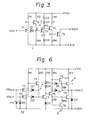
- a logic circuit shown in Fig. 3 is provided with a level-shift circuit 3 consisting of series-connected diodes D3 and D4 between the resistor R3 at the collector of the transistor T3 and the power supply, in addition to the logic circuit of Fig. l.
- Other circuit elements of the logic circuit of Fig. 3 are substantially identical to those in Fig. l.
- the level-shift circuit 3 is provided to enable an increase in a forward voltage VFl for the transistors T4 and T5 to a level higher than another forward voltage VF2 for the transistors T2 and T3. Therefore, due to the provision of the level-shift circuit 3, an unstable operation of the output transistor T5 is avoided upon a start-up of the power supply, as will be seen later.
- a line V CC indicates the rise of the voltage V CC of the power supply
- curves CV A , CV B , CV C , CV D , CV E and CV F indicate voltage changes V A , V B , V C , V D , V E and V F at nodes A, B, C, D, E, and F in Fig. 3.
- Figures 5a to 5d are timing charts of the operations of the transistors T2 to T5.
- the transistor Tl is inversion-biased between the base and the emitter thereof, and thus the transistor T2 and the transistor T3 are turned OFF.
- the diode D2 is nonconductive.
- V A V BET2 + V BET3 + V FD2 ... (l)
- the voltage V CC at the base of transistor T4 is abruptly increased on the basis of the Schottky-clamped diode characteristics of the transistor T3.
- the voltage V D reaches the forward voltage of the diode D2 V F2 of approximately 0.8 V at a time t4 , in other words, the voltage V CC reaches approximately 2.4 V
- the voltage V C at the base of the transistor T4 is increased to approximately l.2 V.
- the voltage V C of l.2 V is sufficient to turn ON the transistor T4, and then the transistor T4 is brought to the active ON state at the time t3.
- a current flows through the resistor R4, the collector ⁇ emitter of the transistor T4, and the resistor R6.
- the voltage V E is insufficient to turn ON the transistor T5, and in order to turn the transistor T5 ON, the voltage V CC must be higher than the voltage (V FD3 + V FD4 + V BET4 + V BET3 ) ⁇ 3.2 V, but a current voltage V CC is approximately 2.4 V. Accordingly, the output transistor T5 is kept OFF.
- the voltage V F is increased in response to the rise of the voltage V CC , but is lower than the voltage V CC by a voltage drop VR4 at the resistor R4.
- Other voltages V A , V B , V C , V D and V E are saturated at predetermined levels, determined by the forward voltage of the transistor and/or the diode and the voltage drop at the resistor, respectively.
- the output signal SOUT is high level.
- the input transistor Tl is turned ON during the operation of the logic circuit of Fig. 3, the voltage V A of the base at the transistor T2 is turned OFF during that operation, the transistor T3 is kept OFF, and the diode D2 is nonconductive.
- the voltage V C at the base of the transistor T4 exceeds the voltage V F3 + V F4 + V BET4 , i.e. approximately 2.4 V, and thus the transistor T4 is turned ON.
- a current then flows through the series-diodes D3 and D4, the resistor R3, the base ⁇ emitter of the transistor T4, and the resistor R6 and increases the voltage V E at the base of the transistor T5 in response to the rise of the voltage V CC .
- the output transistor T5 When the voltage V E exceeds the threshold voltage V TH5 of approximately 0.8 V, in other words, the voltage V CC exceeds the voltage (V FD3 + V FD4 + V BET4 + V BET5 ) of approximately 3.2 V, the output transistor T5 is turned ON. If the pull-up resistor R PL and the load 2 are connected to the collector of the transistor T5, the output signal SOUT is low level.
- An effective low level output signal is output after the voltage V CC has exceeded (V FD3 + V FD4 + V BET4 + B BET5 ), but the undesirable pulse output is not inhibited.
- the logic circuit shown in Fig. 6 includes an input circuit la, an off buffer circuit 4, and an active pull-down circuit 5.
- the input circuit la consists of parallel-connected input PNP-type bipolar transistors Tll and Tl2, parallel-connected Schottky barrier clamping diodes Dl3 and Dl4, parallel-connected speed-up Schottky barrier diodes Dll and Dl2, the NPN-type Schottky-clamped bipolar transistor T2, and the resistors Rl and R2.
- the off buffer circuit 5 consists of an NPN-type Schottky-clamped bipolar transistor T6, an NPN-type bipolar transistor T7, Schottky barrier diodes D6 and D7, and resistors R7 and R8.
- the active pull-down circuit 5 consists of an NPN-type Schottky-clamped bipolar transistor T8, the resistor R6, and a resistor R9.
- the logic circuit of Fig. 6 includes a Schottky barrier diode D5 connected in parallel to the output transistor T5.
- Other circuit elements are substantially the same as those shown in Fig. 3.
- the input circuit la functions as a two-input AND gate.
- the off buffer circuit 4, per se, is known as a current drive circuit for an input circuit of a TTL circuit and improves an operational margin against noise, etc., the diode D5 protects the transistor T5 against noise, and the active pull-down circuit 5 contributes to the speed-up of the transistor T4. These circuits can selectively be adopted.
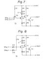
- the logic circuit shown in Fig. 7 includes an input circuit lb, consisting of the resistor R2 and a multi-emitter NPN-type bipolar transistor Tl3, and NPN-type bipolar transistors T3 ⁇ , T4 ⁇ and T5 ⁇ instead of the NPN-type Schottky-clamped bipolar transistors T3, T4 and T5 in Fig. 3.
- the level-shift diode D2 for the transistor T3 ⁇ , the level-shift circuit 3 for the transistor T4 ⁇ , and the resistors R3, R4, and R6 are substantially identical to those shown in Fig. 3.
- the logic circuit in Fig. 6 operates a two input AND buffer circuit, and the principle of the buffer operation is the same as that of Fig. 3.
- the logic circuit shown in Fig. 6 includes an input circuit lc consisting of two Schottky barrier diodes Dl5 and Dl6 and the resistor R2.
- the input circuit lc also functions as a two input AND circuit.
- the other circuits are substantially the same as those in Fig. 3.
- the logic circuit is made stable against transient changes in the voltage V CC of the power supply.
Landscapes
- Engineering & Computer Science (AREA)
- Physics & Mathematics (AREA)
- Computer Hardware Design (AREA)
- Computing Systems (AREA)
- General Engineering & Computer Science (AREA)
- Mathematical Physics (AREA)
- Power Engineering (AREA)
- Logic Circuits (AREA)
Applications Claiming Priority (2)
| Application Number | Priority Date | Filing Date | Title |
|---|---|---|---|
| JP61160268A JPS6315523A (ja) | 1986-07-08 | 1986-07-08 | 論理回路 |
| JP160268/86 | 1986-07-08 |
Publications (2)
| Publication Number | Publication Date |
|---|---|
| EP0253555A2 true EP0253555A2 (de) | 1988-01-20 |
| EP0253555A3 EP0253555A3 (de) | 1989-07-05 |
Family
ID=15711325
Family Applications (1)
| Application Number | Title | Priority Date | Filing Date |
|---|---|---|---|
| EP87305986A Withdrawn EP0253555A3 (de) | 1986-07-08 | 1987-07-07 | Logische Schaltung mit bipolaren Transistoren, die sich während der Speisespannungsanlaufszeitstabil verhält |
Country Status (3)
| Country | Link |
|---|---|
| EP (1) | EP0253555A3 (de) |
| JP (1) | JPS6315523A (de) |
| KR (1) | KR900005461B1 (de) |
Cited By (1)
| Publication number | Priority date | Publication date | Assignee | Title |
|---|---|---|---|---|
| US6008687A (en) * | 1988-08-29 | 1999-12-28 | Hitachi, Ltd. | Switching circuit and display device using the same |
Family Cites Families (4)
| Publication number | Priority date | Publication date | Assignee | Title |
|---|---|---|---|---|
| GB1388437A (en) * | 1972-08-25 | 1975-03-26 | Nat Res Dev | Electronic switching circuits |
| JPS601980B2 (ja) * | 1979-05-23 | 1985-01-18 | 富士通株式会社 | 自動リセット回路 |
| DE3377185D1 (en) * | 1982-04-21 | 1988-07-28 | Toshiba Kk | Transistor circuit |
| US4609832A (en) * | 1983-10-14 | 1986-09-02 | Sundstrand Corporation | Incremental base drive circuit for a power transistor |
-
1986
- 1986-07-08 JP JP61160268A patent/JPS6315523A/ja active Pending
-
1987
- 1987-07-07 EP EP87305986A patent/EP0253555A3/de not_active Withdrawn
- 1987-07-08 KR KR8707327A patent/KR900005461B1/ko not_active Expired
Cited By (1)
| Publication number | Priority date | Publication date | Assignee | Title |
|---|---|---|---|---|
| US6008687A (en) * | 1988-08-29 | 1999-12-28 | Hitachi, Ltd. | Switching circuit and display device using the same |
Also Published As
| Publication number | Publication date |
|---|---|
| JPS6315523A (ja) | 1988-01-22 |
| KR900005461B1 (en) | 1990-07-30 |
| EP0253555A3 (de) | 1989-07-05 |
Similar Documents
| Publication | Publication Date | Title |
|---|---|---|
| EP0367612B1 (de) | Lastgesteuerter ECL-Treiber | |
| KR910009086B1 (ko) | 출력회로 | |
| US5089724A (en) | High-speed low-power ECL/NTL circuits with AC-coupled complementary push-pull output stage | |
| EP0239762A2 (de) | Pufferschaltung | |
| US4437021A (en) | Line driver circuit | |
| US4289978A (en) | Complementary transistor inverting emitter follower circuit | |
| US4250407A (en) | Multi function patch pin circuit | |
| US3571616A (en) | Logic circuit | |
| EP0046498A1 (de) | Bootstrap-Treiberschaltung | |
| EP0253555A2 (de) | Logische Schaltung mit bipolaren Transistoren, die sich während der Speisespannungsanlaufszeitstabil verhält | |
| EP0285157A2 (de) | Tri-state-Ausgangsschaltung | |
| US5514984A (en) | Active pull down type ECL apparatus capable of stable operation | |
| US5066874A (en) | Signal output circuit having bipolar transistor in output stage and arranged in cmos semiconductor integrated circuit | |
| US4242605A (en) | Transient array drive for bipolar ROM/PROM | |
| JPH03227119A (ja) | Ecl論理回路 | |
| EP0465167B1 (de) | Schwellenfreie logische Schaltung | |
| EP0285068A3 (de) | Logikschaltung | |
| EP0299581A2 (de) | Bipolar-Multiplexer mit Verwendung einer Wähl-Pufferschaltung | |
| EP0155305B1 (de) | Am ausstrahlerkollektor gekuppelte logische schaltung | |
| US4682056A (en) | Switching circuit having low speed/power product | |
| EP0219040B1 (de) | Schaltung zum Beschleunigen der ansteigenden Übergänge in TTL- oder DTL-Schaltungen mit hoher kapazitiver Belastung | |
| EP0149075A2 (de) | Vorübergehender Wechselstromtreiber für Speicherzellen | |
| EP0614280B1 (de) | Integrierte Halbleiterschaltung | |
| JP3233473B2 (ja) | 電圧レベル変換回路 | |
| JPH0661436A (ja) | Ttl−cmos出力段 |
Legal Events
| Date | Code | Title | Description |
|---|---|---|---|
| PUAI | Public reference made under article 153(3) epc to a published international application that has entered the european phase |
Free format text: ORIGINAL CODE: 0009012 |
|
| AK | Designated contracting states |
Kind code of ref document: A2 Designated state(s): DE FR GB |
|
| PUAL | Search report despatched |
Free format text: ORIGINAL CODE: 0009013 |
|
| AK | Designated contracting states |
Kind code of ref document: A3 Designated state(s): DE FR GB |
|
| STAA | Information on the status of an ep patent application or granted ep patent |
Free format text: STATUS: THE APPLICATION IS DEEMED TO BE WITHDRAWN |
|
| 18D | Application deemed to be withdrawn |
Effective date: 19900106 |
|
| RIN1 | Information on inventor provided before grant (corrected) |
Inventor name: YASUDA, YASUSHI Inventor name: ENOMOTO, HIROMU Inventor name: TAHARA, AKINORI Inventor name: KUMAGAI, MASAO |