EP0253732A1 - Versorgungseinrichtung für Entladungslampen - Google Patents
Versorgungseinrichtung für Entladungslampen Download PDFInfo
- Publication number
- EP0253732A1 EP0253732A1 EP87401661A EP87401661A EP0253732A1 EP 0253732 A1 EP0253732 A1 EP 0253732A1 EP 87401661 A EP87401661 A EP 87401661A EP 87401661 A EP87401661 A EP 87401661A EP 0253732 A1 EP0253732 A1 EP 0253732A1
- Authority
- EP
- European Patent Office
- Prior art keywords
- circuit
- lamp
- current
- self
- transformer
- Prior art date
- Legal status (The legal status is an assumption and is not a legal conclusion. Google has not performed a legal analysis and makes no representation as to the accuracy of the status listed.)
- Withdrawn
Links
- 239000003990 capacitor Substances 0.000 claims description 12
- 230000001105 regulatory effect Effects 0.000 claims description 6
- 230000003071 parasitic effect Effects 0.000 claims description 3
- 230000037452 priming Effects 0.000 claims description 3
- 229910000859 α-Fe Inorganic materials 0.000 claims description 3
- 230000005294 ferromagnetic effect Effects 0.000 claims description 2
- 230000001681 protective effect Effects 0.000 claims 1
- 238000011084 recovery Methods 0.000 claims 1
- 229910052736 halogen Inorganic materials 0.000 abstract description 5
- DGAQECJNVWCQMB-PUAWFVPOSA-M Ilexoside XXIX Chemical compound C[C@@H]1CC[C@@]2(CC[C@@]3(C(=CC[C@H]4[C@]3(CC[C@@H]5[C@@]4(CC[C@@H](C5(C)C)OS(=O)(=O)[O-])C)C)[C@@H]2[C@]1(C)O)C)C(=O)O[C@H]6[C@@H]([C@H]([C@@H]([C@H](O6)CO)O)O)O.[Na+] DGAQECJNVWCQMB-PUAWFVPOSA-M 0.000 abstract description 3
- 150000002367 halogens Chemical class 0.000 abstract description 3
- 229910052708 sodium Inorganic materials 0.000 abstract description 3
- 239000011734 sodium Substances 0.000 abstract description 3
- QSHDDOUJBYECFT-UHFFFAOYSA-N mercury Chemical compound [Hg] QSHDDOUJBYECFT-UHFFFAOYSA-N 0.000 abstract description 2
- 229910052754 neon Inorganic materials 0.000 abstract description 2
- GKAOGPIIYCISHV-UHFFFAOYSA-N neon atom Chemical compound [Ne] GKAOGPIIYCISHV-UHFFFAOYSA-N 0.000 abstract description 2
- 229910052753 mercury Inorganic materials 0.000 abstract 1
- 229910001511 metal iodide Inorganic materials 0.000 abstract 1
- 238000004804 winding Methods 0.000 description 22
- 229910052757 nitrogen Inorganic materials 0.000 description 5
- 229910052698 phosphorus Inorganic materials 0.000 description 5
- 230000033228 biological regulation Effects 0.000 description 4
- 230000000694 effects Effects 0.000 description 4
- 230000007423 decrease Effects 0.000 description 3
- 238000010586 diagram Methods 0.000 description 3
- 230000005291 magnetic effect Effects 0.000 description 3
- -1 metal halide halogen Chemical class 0.000 description 3
- 238000006243 chemical reaction Methods 0.000 description 2
- 230000001939 inductive effect Effects 0.000 description 2
- 238000002955 isolation Methods 0.000 description 2
- 229910001507 metal halide Inorganic materials 0.000 description 2
- 230000010355 oscillation Effects 0.000 description 2
- 238000010521 absorption reaction Methods 0.000 description 1
- 230000037213 diet Effects 0.000 description 1
- 235000005911 diet Nutrition 0.000 description 1
- 230000009977 dual effect Effects 0.000 description 1
- 238000010616 electrical installation Methods 0.000 description 1
- 238000001914 filtration Methods 0.000 description 1
- 238000009499 grossing Methods 0.000 description 1
- 230000017525 heat dissipation Effects 0.000 description 1
- FFUAGWLWBBFQJT-UHFFFAOYSA-N hexamethyldisilazane Chemical compound C[Si](C)(C)N[Si](C)(C)C FFUAGWLWBBFQJT-UHFFFAOYSA-N 0.000 description 1
- 230000006698 induction Effects 0.000 description 1
- 239000003999 initiator Substances 0.000 description 1
- 238000009434 installation Methods 0.000 description 1
- 238000004519 manufacturing process Methods 0.000 description 1
- ORQBXQOJMQIAOY-UHFFFAOYSA-N nobelium Chemical compound [No] ORQBXQOJMQIAOY-UHFFFAOYSA-N 0.000 description 1
- 230000010287 polarization Effects 0.000 description 1
- 230000002459 sustained effect Effects 0.000 description 1
- 230000009466 transformation Effects 0.000 description 1
- 230000001131 transforming effect Effects 0.000 description 1
Images


Classifications
-
- H—ELECTRICITY
- H05—ELECTRIC TECHNIQUES NOT OTHERWISE PROVIDED FOR
- H05B—ELECTRIC HEATING; ELECTRIC LIGHT SOURCES NOT OTHERWISE PROVIDED FOR; CIRCUIT ARRANGEMENTS FOR ELECTRIC LIGHT SOURCES, IN GENERAL
- H05B41/00—Circuit arrangements or apparatus for igniting or operating discharge lamps
- H05B41/14—Circuit arrangements
- H05B41/26—Circuit arrangements in which the lamp is fed by power derived from DC by means of a converter, e.g. by high-voltage DC
- H05B41/28—Circuit arrangements in which the lamp is fed by power derived from DC by means of a converter, e.g. by high-voltage DC using static converters
- H05B41/282—Circuit arrangements in which the lamp is fed by power derived from DC by means of a converter, e.g. by high-voltage DC using static converters with semiconductor devices
- H05B41/2821—Circuit arrangements in which the lamp is fed by power derived from DC by means of a converter, e.g. by high-voltage DC using static converters with semiconductor devices by means of a single-switch converter or a parallel push-pull converter in the final stage
- H05B41/2822—Circuit arrangements in which the lamp is fed by power derived from DC by means of a converter, e.g. by high-voltage DC using static converters with semiconductor devices by means of a single-switch converter or a parallel push-pull converter in the final stage using specially adapted components in the load circuit, e.g. feed-back transformers, piezoelectric transformers; using specially adapted load circuit configurations
-
- Y—GENERAL TAGGING OF NEW TECHNOLOGICAL DEVELOPMENTS; GENERAL TAGGING OF CROSS-SECTIONAL TECHNOLOGIES SPANNING OVER SEVERAL SECTIONS OF THE IPC; TECHNICAL SUBJECTS COVERED BY FORMER USPC CROSS-REFERENCE ART COLLECTIONS [XRACs] AND DIGESTS
- Y02—TECHNOLOGIES OR APPLICATIONS FOR MITIGATION OR ADAPTATION AGAINST CLIMATE CHANGE
- Y02B—CLIMATE CHANGE MITIGATION TECHNOLOGIES RELATED TO BUILDINGS, e.g. HOUSING, HOUSE APPLIANCES OR RELATED END-USER APPLICATIONS
- Y02B20/00—Energy efficient lighting technologies, e.g. halogen lamps or gas discharge lamps
Definitions
- the subject of the present invention is a device for supplying lamps, discharge lamps, discharge tubes, etc. of the halogen, metal halide halogen, sodium vapor, mercury vapor, ultraviolet, neon, etc. type. .
- these lamps or tubes cannot be connected directly to the network of the electrical installation, they must be connected, either in series with a current regulating impedance (generally inductive), or with a reducing or raising voltage transformer with or without galvanic isolation, either with a combination of these two elements.
- a current regulating impedance generally inductive
- a reducing or raising voltage transformer with or without galvanic isolation
- the device object of the invention overcomes these drawbacks; moreover, it substantially attenuates the stroboscopic effect with regard to discharge lamps and tubes, hence greater comfort of use and energy saving.
- This device conforms to claim 1.
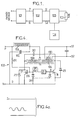
- FIG. 1 shows a device for feeding a tube 100 according to the invention which comprises: - a connection element on the alternative network 101 which is indifferent to the frequency of the network; - a self-oscillating generator 102 of sine power voltage, at frequencies higher than those of the network, of the order of 10 to 100 KHz operating in class C or B and connected to the output P and N terminals of the item 101; a current regulator circuit 103 of the lamp or of the tube, connected to the output terminals S1 and S2 of the element 102, and - an ignition circuit 104 for discharge lamps or tubes in cases requiring a high voltage of the order of 2,500 to 4,000 V.
- connection circuit 101 on the alternating network usually at 50 Hz or 60 Hz (see fig. 2) includes: - a peak current limiting circuit 1 which is self-inductive and which also allows parasitic decoupling of the circuit vis-à-vis the network.
- This circuit comprises at least one series choke 1A, 1B, with an air gap limiting the appropriate saturation current (fig. 2).
- Parasitic decoupling of the circuit from the network is carried out with capacitors 2 and 3 in combination with the series reactors 1A and 1B - a rectifier bridge 4 - a filtering (or smoothing) capacitor 5A and / or 5B which makes it possible to obtain a filtered DC voltage between points P and N.
- connection element on the AC network is characterized by the fact that it has a relatively high input choke impedance, thus attenuating the incidence of the capacity 5A, 5B which is generally of high value. It thus allows the absorption of a lower peak current and a longer duration on the network; therefore, it can be more easily controlled by switching or scaling triacs.
- the two inductors with air gaps 1A and 1B are of opposite polarity, which makes it possible to add the impedance of one to that of the other.
- FIG. 3 One of the possible embodiments of the sinusoidal voltage generator is presented in FIG. 3.
- This mono-alternation realization includes: - at least one transformer 14, having at least two windings 14A and 14B (14C etc.). - At least one resonance capacity 15, in parallel on the winding 14A among others. - a switching transistor 7. - an anti-resonance self 13. - a resistor 6, connected between point P and point 7B, which has the purpose of creating a leakage current between points 7C and 7E of transistor 7. - a diode 8. - a resistance 9. - a diode 10, in series with the resistor 9. a capacity 11, in series with the winding 14B, so that the capacity 11 and winding 14B assembly is in parallel with the points 7E and 7B. - a diode 16.
- the transformer 14, the transistor 7 and the choke 13 are the three essential elements; they are mounted in series, in any order, so that the assembly is in parallel with points P and N.
- the current created by the resistor 6 generates a known resonance phenomenon between the winding 14A and the capacitor 15.
- the current thus generated is taken up by the reaction winding 14B and amplified by the transistor 7, thus creating sustained oscillations.
- the generator When powering up, the generator first oscillates in class A, then it quickly switches to class B, to reach its operating speed in class C, all in a few fractions of seconds.
- winding 14B The purpose of the winding 14B is to create the reaction and to maintain the oscillation.
- the purpose of the capacitance 11 is, on the one hand, to present a series impedance between the point 7B, the winding 14B and point 7E, on the other hand, create a negative bias of 7B with respect to 7E.
- transistor 7 depends on the negative polarity of point 7B with respect to 7E.
- the purpose of the resistor 9 is to evacuate these negative charges towards point 7E.
- the purpose of the presence of the diode 10 is to neutralize the impact of the resistor 9 on the resistor 6.
- the inductor 13 has the effect of making the incidence of the capacitor 15 negligible and of facilitating the saturation of the transistor 7 during its conduction.
- the choke 13 has the major drawback of generating, in many cases of use, high voltages capable of destroying the transistor 7. To avoid this problem, various means known to this can be used. day in order to reduce the coefficiant Q of the self 13, which inevitably leads to a significant energy loss.
- a winding 13B has been created on the choke 13, of an appropriate polarity; this coil 13B is connected in parallel with the points P and N and in series with the diode 16. The combination coil 13B and diode 16 recovers the overvoltage thus generated.
- Figure 4 shows a variant of the sinusoidal voltage generator, but in full dual alternation operating in class B, that is to say in such a way that the current is never interrupted in the system (see Fig. 4a).
- the current flowing in the oscillating circuit is never interrupted, the variation of the charge being reflected in a variation of the direct current with a slight alternating component.
- the device thus presented comprises: - at least two transistors 17-18 - a transformer 19 - at least three windings 19A, 19B, 19C and if necessary a fourth winding 19 D (or more) for the connection of the load, if galvanic isolation is desired. - At least one capacity 20 in parallel on at least one of the windings for resonance. - a resistance 22 - a diode 23 - resistance 24 - an impedance 21 which is sometimes necessary to limit the current in the circuit. Indeed, beyond a limited voltage, inherent in the type of transistor used, a Zener effect occurs and causes a very high current between points 18B and 17B.
- Impedance 21 can be ohmic, capacitive, selfic, or a combination of the two, or even of the three.
- the two transistors 17-18 drive alternately, that is to say that the increase in current in one necessarily results in a decrease in the other, and aims and vice versa.
- the defined NPN bi-polar transistors can be of PNP, MOS, GOT, etc. type, without departing from the scope of the invention, it suffices to apply the appropriate polarizations, which is within the reach of those skilled in the art.
- the device which is the subject of the invention also provides a series impedance between the power source and the load in question, in order on the one hand to regulate the current and on the other hand to decouple the oscillating system from the load and of its variation.
- the most appropriate series impedance is a selfic impedance (see Fig. 5).
- This inductive impedance 30 comprises at least one winding (wound on a ferromagnetic body, for example ferrite), connected in series between the load and the power source. Therefore, if the load decreases in resistance for any reason, this decrease has little effect on the value of the voltage generated at the terminals of the transformer defined above, and the system continues to function perfectly.
- a capacitor 32 is placed in parallel with the load. This allows, on the one hand, a correction of the power factor between open circuit voltage and loaded voltage which is useful as soon as the latter varies by a factor greater than 1.5 compared to the open circuit voltage and, d on the other hand, better protection of the transistors of the self-oscillating generator.
- This sensitive element 31 can be a photo-diode, a photo-resistance, a photo-transistor or a current transformer, etc ...
- the choke 30 can be materialized by a winding of wire around a magnetic body of ferrite type or similar of any shape, or quite simply materialized by a magnetic leak between primary and secondary (See Figure 7 hatched part 33).
- the discharge lamp or tube
- a high voltage of the order of 2500 to 4000 volts and even more (see manufacturer's instructions), which is generally the case for halogen metal halide lamps, high pressure sodium, ultraviolet, etc ...
- an initiator which can if necessary be added to or incorporated into the diet.
- Fig. 5 shows a possible starting device within the framework of the invention.
- This device includes: - A current regulating choke 70 (which can be the same as that defined in FIGS. 5 or 6), having at least two windings 70A and 70B; winding 70A is used to regulate the current of the lamp and in the absence of current to raise the voltage to the few thousand volts required; winding 70B is used to generate a voltage of the order of 100 to 250 volts, which is high by the transformation ratio between 70A and 70B.
- - a diode 71 which serves to rectify the voltage at the terminals of the lamp (or tube) in the absence of current.
- - a capacitor 72 which stores this voltage (rectified by the diode 71)
- a resistor 73 which serves to limit this current and to decouple the ignition pulses.
- two resistors 74 and 75 which serve as a voltage divider.
- the capacitor 72 will therefore be gradually charged by the diode 71 and the resistor 73, reaching a critical value, triggering an anode-cathode current of the thyristor 76.
- the thyristor starts to conduct and discharge the capacitor 72 through the winding 70b.
- the trigger threshold of thyristor 76 is determined by its trigger current and by the values of resistors 74, 75, and 73.
- the capacity 77 only has the role of protecting the diode 71 from a reverse voltage generated. This capacity can be useless if one chooses a diode 71 having a reverse voltage of the order of 4000 Volts or more. But this type of diode is more expensive than the capacitance.
- This ignition system is designed to operate in the absence of current in the lamp, resulting in a maximum voltage.
- the voltage is found to be about half of the maximum voltage.
- resistors 74, 75 and 73 are such that the system operates satisfactorily at a voltage of the order of 70 to 100% of the maximum voltage (voltage in the absence of current); the system is interrupted during normal lamp operation.
- the thyristor 76 can be replaced by any other element shorting out at a predetermined voltage, of the SIDAC, TRISIL type, etc.
- This device can find a large field of applications in lighting, industry, the medical field, etc. It can be an advantageous replacement for existing systems at an equal and even lower production cost.
Landscapes
- Engineering & Computer Science (AREA)
- Power Engineering (AREA)
- Circuit Arrangements For Discharge Lamps (AREA)
Applications Claiming Priority (2)
| Application Number | Priority Date | Filing Date | Title |
|---|---|---|---|
| FR8610248A FR2601840A1 (fr) | 1986-07-15 | 1986-07-15 | Dispositif electronique d'alimentation de lampes, lampes a decharge, tubes a decharge, etc. |
| FR8610248 | 1986-07-15 |
Publications (1)
| Publication Number | Publication Date |
|---|---|
| EP0253732A1 true EP0253732A1 (de) | 1988-01-20 |
Family
ID=9337419
Family Applications (1)
| Application Number | Title | Priority Date | Filing Date |
|---|---|---|---|
| EP87401661A Withdrawn EP0253732A1 (de) | 1986-07-15 | 1987-07-15 | Versorgungseinrichtung für Entladungslampen |
Country Status (2)
| Country | Link |
|---|---|
| EP (1) | EP0253732A1 (de) |
| FR (1) | FR2601840A1 (de) |
Citations (4)
| Publication number | Priority date | Publication date | Assignee | Title |
|---|---|---|---|---|
| US3700956A (en) * | 1971-01-04 | 1972-10-24 | Gte Laboratories Inc | Arc discharge lamp control circuit |
| US4329627A (en) * | 1976-02-02 | 1982-05-11 | Esquire, Inc. | High frequency thyristor circuit for energizing a gaseous discharge lamp |
| US4572988A (en) * | 1983-08-22 | 1986-02-25 | Industrial Design Associates, (Ida) | High frequency ballast circuit |
| EP0198632A2 (de) * | 1985-04-04 | 1986-10-22 | Chwee Tor Lee | Elektronisches Vorschaltgerät für Leuchtstofflampen |
Family Cites Families (3)
| Publication number | Priority date | Publication date | Assignee | Title |
|---|---|---|---|---|
| US3165668A (en) * | 1962-12-17 | 1965-01-12 | Gen Electric | Apparatus employing negative resistance device for operating electric discharge lamps |
| US4506195A (en) * | 1983-02-04 | 1985-03-19 | North American Philips Lighting Corporation | Apparatus for operating HID lamp at high frequency with high power factor and for providing standby lighting |
| US4562384A (en) * | 1983-04-19 | 1985-12-31 | General Electric Company | Variable reactance inductor with adjustable ranges |
-
1986
- 1986-07-15 FR FR8610248A patent/FR2601840A1/fr not_active Withdrawn
-
1987
- 1987-07-15 EP EP87401661A patent/EP0253732A1/de not_active Withdrawn
Patent Citations (4)
| Publication number | Priority date | Publication date | Assignee | Title |
|---|---|---|---|---|
| US3700956A (en) * | 1971-01-04 | 1972-10-24 | Gte Laboratories Inc | Arc discharge lamp control circuit |
| US4329627A (en) * | 1976-02-02 | 1982-05-11 | Esquire, Inc. | High frequency thyristor circuit for energizing a gaseous discharge lamp |
| US4572988A (en) * | 1983-08-22 | 1986-02-25 | Industrial Design Associates, (Ida) | High frequency ballast circuit |
| EP0198632A2 (de) * | 1985-04-04 | 1986-10-22 | Chwee Tor Lee | Elektronisches Vorschaltgerät für Leuchtstofflampen |
Also Published As
| Publication number | Publication date |
|---|---|
| FR2601840A1 (fr) | 1988-01-22 |
Similar Documents
| Publication | Publication Date | Title |
|---|---|---|
| US7880399B2 (en) | Ballast for at least one fluorescent high pressure discharge lamp, method for operating said lamp and lighting system comprising said lamp | |
| US6724152B2 (en) | Lighting control system with variable arc control including start-up circuit for providing a bias voltage supply | |
| US4132925A (en) | Direct current ballasting and starting circuitry for gaseous discharge lamps | |
| US4168453A (en) | Variable intensity control apparatus for operating a gas discharge lamp | |
| GB2104318A (en) | Starting and operating loads with changing impedance characteristics | |
| FR2627342A1 (fr) | Dispositif d'alimentation de tube luminescent | |
| EP0918449B1 (de) | Schaltung zur Steuerung einer Leuchtstofflampe | |
| US5619106A (en) | Diodeless start circiut for gas discharge lamp having a voltage divider connected across the switching element of the inverter | |
| US6157142A (en) | Hid ballast circuit with arc stabilization | |
| JPH05144584A (ja) | 汎用電子バラスト装置 | |
| US5373215A (en) | Ionization tube simmer current circuit | |
| EP0253732A1 (de) | Versorgungseinrichtung für Entladungslampen | |
| US4282462A (en) | Arc lamp lighting unit with means to prevent prolonged application of starting potentials | |
| CA1110315A (en) | Operating circuit for flash lamp directly coupled to ac source | |
| EP0078722A1 (de) | Elektronische Speisungseinrichtung die aus dem Wechselstromnetz einen sinusförmigen, sich mit der Spannung in Phase befindenden Strom aufnimmt | |
| JPS59136028A (ja) | 直流安定化電源の保護装置 | |
| JPH05260736A (ja) | スイッチングレギュレータ | |
| SU1246065A1 (ru) | Устройство дл ограничени напр жени | |
| US20060103326A1 (en) | Variable frequency half bridge driver | |
| EP0946081A1 (de) | Anordnung zum Betreiben einer Entladungslampe in einem Kraftfahrzeugscheinwerfer | |
| EP1324478A2 (de) | Hochspannungswandler mit schneller Antwortzeit | |
| JP3378117B2 (ja) | 点灯装置 | |
| CA1156303A (en) | Keep-alive circuit for gas discharge lamp | |
| SU570225A1 (ru) | Устройство дл зажигани газоразр дных ламп | |
| JPS6115600Y2 (de) |
Legal Events
| Date | Code | Title | Description |
|---|---|---|---|
| PUAI | Public reference made under article 153(3) epc to a published international application that has entered the european phase |
Free format text: ORIGINAL CODE: 0009012 |
|
| AK | Designated contracting states |
Kind code of ref document: A1 Designated state(s): BE CH DE GB IT LI |
|
| STAA | Information on the status of an ep patent application or granted ep patent |
Free format text: STATUS: THE APPLICATION IS DEEMED TO BE WITHDRAWN |
|
| 18D | Application deemed to be withdrawn |
Effective date: 19880721 |
|
| RIN1 | Information on inventor provided before grant (corrected) |
Inventor name: KNEIDER, FRANCOIS |