EP0255857A2 - Mehrfachrechnersystem - Google Patents
Mehrfachrechnersystem Download PDFInfo
- Publication number
- EP0255857A2 EP0255857A2 EP87107576A EP87107576A EP0255857A2 EP 0255857 A2 EP0255857 A2 EP 0255857A2 EP 87107576 A EP87107576 A EP 87107576A EP 87107576 A EP87107576 A EP 87107576A EP 0255857 A2 EP0255857 A2 EP 0255857A2
- Authority
- EP
- European Patent Office
- Prior art keywords
- processor
- program
- identification code
- processors
- outputted
- Prior art date
- Legal status (The legal status is an assumption and is not a legal conclusion. Google has not performed a legal analysis and makes no representation as to the accuracy of the status listed.)
- Granted
Links
Images



Classifications
-
- G—PHYSICS
- G06—COMPUTING OR CALCULATING; COUNTING
- G06F—ELECTRIC DIGITAL DATA PROCESSING
- G06F9/00—Arrangements for program control, e.g. control units
- G06F9/06—Arrangements for program control, e.g. control units using stored programs, i.e. using an internal store of processing equipment to receive or retain programs
- G06F9/46—Multiprogramming arrangements
- G06F9/54—Interprogram communication
-
- G—PHYSICS
- G06—COMPUTING OR CALCULATING; COUNTING
- G06F—ELECTRIC DIGITAL DATA PROCESSING
- G06F15/00—Digital computers in general; Data processing equipment in general
- G06F15/16—Combinations of two or more digital computers each having at least an arithmetic unit, a program unit and a register, e.g. for a simultaneous processing of several programs
- G06F15/161—Computing infrastructure, e.g. computer clusters, blade chassis or hardware partitioning
Definitions
- This invention relates to a parallel processor consisting of a plurality of processors that can operate in parallel with one another.
- a program consisting of the aggregate of units of work is generated and each of the units of work are executed in parallel so that one processing can be executed as a whole.
- This unit of work consists of a program and control information necessary for the execution of the program, but the present invention will hereinafter deal primarily with the program alone. Accordingly, the unit of work will be hereinafter called a "process” and a group of such processes, a "job”.
- processors one or a plurality of groups (jobs) are executed in parallel with one another.
- the present invention is therefore directed to provide a parallel processor system capable of executing such a program which is prepared without determining in advance which process is to be alloted to which processor.
- a parallel processor system which comprises a plurality of processors capable of operating independently of one another and transfer means for transferring the data outputted from any one of the programs during execution of one program by any one of the processors to the other of said processors to which a receiving program is allotted, in response to a program identification code outputted during execution of one program described above by one processor described above in order to identify the receiving program.
- Fig. l shows a first embodiment of a parallel processor system in accordance with the present invention.
- processor (0) ⁇ processor (n)
- the drawing. shows only the processors (0) and (l) for simplification.
- One job consists of a plurality of processes that can be executed in parallel with one another.
- a number called "job number” is assigned to each job.
- the job number is managed in such a manner that each job number is unique in this parallel processor system at each time and different jobs cannot have the same job number.
- a number starting from zero (0) is put to the processes constituting the job and called a "within-job process number".
- a given process can send data to other processes belonging to the same job.
- the within-job process number is designated as the address of the data to be sent.
- the set of the numbers of the former is used to designate the receiving process, and in this data transfer, the set of the numbers of the former is translated to the set of the numbers of the latter and the set of the numbers after translation is used in order to effect data transfer to the processor to which the receiving process is allotted.
- reference numeral 2 represents a host processor
- 3 is an interconnection network for the data transfer between the processors 0 to n
- 4 is a send address translator
- 5 is a receive address translator.
- reference numeral 6 represents a data register
- 7 is a send register
- l0 is a network address generator
- reference numeral 8 represents a receive register
- 9 is a data register
- ll is a within-processor-address generator.
- the host processor 2 is of a program control type processor and programmed in such a manner as to send data to each part of the parallel processor system through channels l4, ll, l2, l3 and to control each processor.
- Each processor l is of a program control type processor which can operate independently of one another, and is formed, for example, by connecting a memory and others to a Microprocessor MC68000 of Motorola Inc.
- Each processor l has a receive buffer l00, which consists of a plurality of fields allotted to the processes executed in that processor, respectively.
- Each processor l is programmed so that when the execution of a given process is started, the processor l gives in advance the job number of the job to which the process belongs to the field 6-A of the data register 6 in the corresponding receive address translator 5 through the channel l5.
- the processor l is programmed so that it outputs the within-job process number of the receiving process and the data to be transferred to the fields 6-B and 6-C of the data register 6 through the channel l6, respectively.
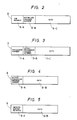
- the content of the data register 6 becomes such as shown in Fig. 2.
- each send address translator 4 outputs the processor number of the processor, in which the process designated by the job number and the within-job processor number given to the fields 6-A and 6-B of the data register 6, respectively, is located, as well as the process number inside that processor for that process, in response to the job number and the within-job processor number described above, and sends them to the fields 7-A and 7-B of the send register 7, respectively.
- the data given to the field 6-C of the data register 6 is as such given to the field 7-C of the send register 7.
- the content of the send register becomes such as shown in Fig. 3.
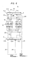
- Fig. 6 shows in detail the send address translator 4.
- the network address generator l0 consists of a memory to which access is made using the job number and the within-job processor number in the fields 6-A and 6-B in the data register 6 as the address and which stores the processor number and within-processor process number of the corresponding processor at its address positions. These data are written in advance by the host processor 2 into this memory through the channels l4, l2 and l3.
- this memory consists of N-order processor number generation memories l2 and N within-processor process number generation memories l3.
- the interconnection network 3 is disposed in order to transfer the content of the send register 7 of the sending processor, such as the processor (0), to the receive register 8 of the receiving processor, such as the processor (l).
- the processor number for the processor (n) is set to the field 7-A in the send register 7 for the processor (0)
- the contents of the fields 7-B and 7-C of the send register 7 for the processor (0) that is, the within-processor process number and the data, are transferred to the fields 8-A and 8-B of the receive register 8 in the receive address translator 5 which is connected to the processor (0), respectively.
- the content of the receive register 8 becomes such as shown in Fig. 4.
- the within-processor-address generator ll in each receive address translator 5 outputs the address of the receive buffer field prepared by the within-processor number given to the field 8-A of the receive register 8 to the field 9-A of the data register 9 in response to the within-processor process number given to the field 8-A.
- the content of the data register 9 becomes such as shown in Fig. 5.
- the data given to the field 8-B of the receive register 8 is transferred as such to the field 9-B of the data register 9 and written into the position represented by the address in the field 9-A in the receive buffer l00 inside that processor.
- the within-processor-address generator ll consists of a memory to which access is made by use of the within-processor process number as the address, for example, and which stores the receive buffer address.
- This receive buffer address is written in advance by the host processor through the channels l4, ll and l3. More definitely, the host processor 2 sets the receive buffer address of the process which is allotted to the processor connected to the receive address translator and has the within-processor process number k, to the k th address of this memory.
- the control program on the host processor 2 Upon receiving the job start command from a user, the control program on the host processor 2 makes the following operations.
- the job on the parallel processor system is started by the operation of the control program on the host processor described above.
- the processor picks up one process that can be executed among the processes allotted thereto, and executes it.
- the operation that does not involve data transfer to the other processes is the same as the operation of an ordinary processor system.
- the processor sends the job number to which the process requesting the data transfer belongs, the process number of the receiving part designated by the program and the data to the fields 6-A, 6-B and 6-C of the send data register 6 in the send address translator 4, respectively.
- the send address translator 4 Upon receiving them, the send address translator 4 determines the processor number to which the receiving process of the data is allotted and the within-processor process number of the receiving process and gives them to the fields 7-A and 7-B of the send register 7. The content of the field 6-C is given as such to the field 7-C. Then, the interconnection network 3 sends the values of the fields 7-B and 7-C of the send register of the sending part to the fields 8-A and 8-B of the receive register 8 in the receive address translator 5 connected to the processor which is designated by the send processor number given by the field 7-A of the send register 7.
- the receive address translator 5 Upon receiving these values, the receive address translator 5 determins the address of the receive buffer region of the process from the within-processor process number given to the field 8-A of the receive register 8 and puts it to the field 9-A of the receive data register 9. It puts the data given to the field 8-B of the receive register 8 to the field 9-B of the receive data register 9. Then, the data of 9-B is written into the address designated by 9-A and data communication is thus complete.
- the allotment condition (l) is satisfied and all the processes belonging to one processor belong to the same job.
- each send address translator 4 makes only address translation relating to one job allotted in advance. Therefore, even if the job number is not designated from the processor, address translation can be made on the basis of the within-processor process number.
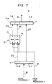
- the network address generator l0 can be composed of a pair of memories consisting of a memory l2 to which access is made by use of the within-processor process number as the address and which outputs the processor number and a memory l3 to which access is made by use of the within-processor process number as the address and outputs the within-processor process number, as shown in Fig. 7.
- the send register 7 may consist of a register devoid of the field 6-A of Fig. l, as shown in Fig. 7. It is possible to eliminate also the channels l5 and ll2 of Fig. l.
- the receive address translator 5 is the same as one shown in Fig. l.
- the send address translator 4 can be constituted by a divider by changing the allotment condition in the following way as shown in Fig. 8.
- Allotment is made under the allotment condition (2). Namely, the number of processes constituting one job is m and the number of processors executing this job is n. The value n is below the number of processors belonging to the parallel processor system.
- m processes are divided into the n groups in the following manner.
- reference numeral l6 represents the divider, which divides the value given to its port A by the value given to its port B and outputs the quotient to the port Q and the remainder to the port R.
- Reference numeral l5 represents a processor number conversion memory.
- Reference numeral l7 represetns a usable-processor-total-number register, and these elements l5 to l7 constitute the network address generator l0. Data are written in advance to this memory l5 by the host processor in the following manner.
- the host processor 2 writes the value n described above into the usable-processor-number register l7 in the send address translator 4 and the number of the processor corresponding to the group of each process described in connection with the allotment method at the position using the group number as the address, as the initial operation of the host processor 2 through the channel l3.
- the register 6 may be one devoid of the field 7-A in the same way as in Fig. 7.
- the usable-processor-number register l7 stores the processor number (n described above) used by the job to which the processes to be executed by the processor connected to the send address translator 4 belongs.
- the receive address translator 5 is exactly the same as the translator shown in Fig. l.
- the operation of the send address translator 4 is as follows.
- This apparatus reproduces the operation of the host processor 2 at the time of process allotment with fidelity.
- the divider l6 divides the within-job process number given to the data register 6 by the number of processors executing the job and gives the quotient Q as the within-processor process number to the field 7-B of the send register 7 through the channel ll5.
- the remainder R represents the group number described above and is used as the address input to the processor number conversion memory l5, and the processor number as its output is given to the field 7-A of the send register 7 through the channel ll4.
- the data given to the send data register 6 are handled in the same way as in the foregoing embodiments.
- the divider l6 can be constituted by a more simplified circuit by limiting the allotment condition of Embodiment 3 in the following manner.
- the same allotment condition as the allotment condition (4) is further limited so that p and q are integers, the within-job process number given by the processor l is data of p-ary representation and the number n of processors allotted to the job is p q .
- the divider can be constituted as a selection circuit (not shown) which outputs the q digits from below of the data of the within-job process number given through the channels ll3 as the remainder and the upper digits as the quotient.
- the send address generator 4 and the receive address generator 5 can be more simplified as shown in Figs. 9A and 9B, respectively.
- the send address translator 4 does not need the job number. Since up to one process is disposed in one processor, the within-processor process number is not necessary, either. Therefore, a memory l2 to which access is made using the within-job process number as address and which outputs the corresponding processor number can be used as the network address generator l0 as shown in Fig. 9A.
- the data register 6 may be one devoid of the field 6-A of the register of Fig. l, as shown in Fig. 9A.
- the send register 7 may be one devoid of the field 7-B of the register l, as shown in Fig. 9A.
- the receive address translator 5 may have only the field 8-B for the data as shown in Fig. 9B. Since it is necessary for the within processor address generator ll to output only a single buffer address, it may consist of the register 23 alone as shown in Fig. 9B.
- the network address generator l0 shown in Fig. l can be constituted not only by the random-access memories shown in Fig. 6 but also of associative memories.
- the parallel processor system executes only one job and only one process is allotted to one processor.
- the within-job process number is made to correspond, in principle, as such to the processor number but if there is any fall-off of the processor number to be used, a number greater than the process number constituting the job is allotted to the processor.
- Fig. l0 shows the send address translator 4 in accordance with this embodiment.
- reference numeral 6 represents the data register
- 7 is the send register
- 2l is the associative memory
- 22 is a selector.
- the associative memory 2l outputs a value representing a truth value to the channel l23 if the value inputted from the channel ll3 is registered, and outputs the value stored as a set with the value inputted from the channel ll3, to the channel l2l. It outputs false at other times.
- the selector outputs the value of the channel 2l to the channel l24 if the value outputted to the channel l23 is the truth value and the value of the channel ll3 to the channel l24 if the value is false.
- the receive address translator 5 is the same as one shown in Fig. 9B.
- the host processor sets the set of the fall-off number and the processor number to be used in place of the former to the associative memory 2l through the channel l3 so that the latter can be associated with and searched by the former.
- the selector 22 sends as such the process number in the data register 6 to the send register 7 and if it is registered, the selector 22 selects the substituting processor number to be outputted from the associative memory 2l and sends it to the send register 7 as the data send processor number.
- the data sent from the network through the channel l8 are stored in the receive data register 9 together with the content of the address register 23 and written into the receive buffer region.
- Fig. ll shows a parallel processor system formed in such a fashion.
- control of processors inside the parallel processor system and distribution of processes are borne by the host processor 2 outside the system, but it is possible in each embodiment described above to provide such functions to one of the processors of the parallel processor system such as the processor l-0 and to eliminate the host processor 2 and the channel l4.
- the send address translator 4 and the receive address translator 5 are independent apparatuses of each other and are assorted to the processor l and the interconnection network 3, but they may be constituted as part of processor or interconnection network.
- the present invention makes it possible to determine the distribution of a plurality of processes that can operate in parallel with one another and make mutual communication to the processors inside the parallel processor system for each job after programming, so that even when the number of processors of the parallel processing system changes, processing can be executed as such without any change.
- the present invention can correctly execute multi-job.
Landscapes
- Engineering & Computer Science (AREA)
- Theoretical Computer Science (AREA)
- Physics & Mathematics (AREA)
- Computer Hardware Design (AREA)
- General Engineering & Computer Science (AREA)
- Software Systems (AREA)
- General Physics & Mathematics (AREA)
- Mathematical Physics (AREA)
- Multi Processors (AREA)
Applications Claiming Priority (2)
| Application Number | Priority Date | Filing Date | Title |
|---|---|---|---|
| JP117351/86 | 1986-05-23 | ||
| JP61117351A JP2738674B2 (ja) | 1986-05-23 | 1986-05-23 | 並列計算機及び並列計算機のデータ転送方法 |
Publications (3)
| Publication Number | Publication Date |
|---|---|
| EP0255857A2 true EP0255857A2 (de) | 1988-02-17 |
| EP0255857A3 EP0255857A3 (en) | 1990-10-31 |
| EP0255857B1 EP0255857B1 (de) | 1994-09-14 |
Family
ID=14709539
Family Applications (1)
| Application Number | Title | Priority Date | Filing Date |
|---|---|---|---|
| EP19870107576 Expired - Lifetime EP0255857B1 (de) | 1986-05-23 | 1987-05-22 | Mehrfachrechnersystem |
Country Status (3)
| Country | Link |
|---|---|
| EP (1) | EP0255857B1 (de) |
| JP (1) | JP2738674B2 (de) |
| DE (1) | DE3750530D1 (de) |
Cited By (5)
| Publication number | Priority date | Publication date | Assignee | Title |
|---|---|---|---|---|
| EP0690384A3 (de) * | 1994-06-30 | 1997-08-06 | Nec Corp | Multiprozessorsystem zur lokalen Verwaltung von Adressenübersetzungstabellen |
| GB2501572A (en) * | 2012-06-08 | 2013-10-30 | Mark Henrik Sandstrom | Parallel processing system with hardware routing based on the destination program instance of a packet |
| US10133599B1 (en) | 2011-11-04 | 2018-11-20 | Throughputer, Inc. | Application load adaptive multi-stage parallel data processing architecture |
| US10318353B2 (en) | 2011-07-15 | 2019-06-11 | Mark Henrik Sandstrom | Concurrent program execution optimization |
| CN112585624A (zh) * | 2018-08-23 | 2021-03-30 | 三星电子株式会社 | 使用多个处理器处理神经网络模型的电子装置及其操作方法 |
Families Citing this family (3)
| Publication number | Priority date | Publication date | Assignee | Title |
|---|---|---|---|---|
| JPH06266683A (ja) * | 1993-03-12 | 1994-09-22 | Toshiba Corp | 並列処理装置 |
| JPH0830571A (ja) * | 1995-07-24 | 1996-02-02 | Hitachi Ltd | データ転送ネットワーク |
| JP5182792B2 (ja) * | 2007-10-07 | 2013-04-17 | アルパイン株式会社 | マルチコアプロセッサ制御方法及び装置 |
Family Cites Families (2)
| Publication number | Priority date | Publication date | Assignee | Title |
|---|---|---|---|---|
| US4413318A (en) * | 1980-11-20 | 1983-11-01 | International Business Machines Corporation | Use of nodes to uniquely identify processes |
| EP0137804A4 (de) * | 1983-02-07 | 1987-10-12 | American Telephone & Telegraph | Datennetzschnittstelle. |
-
1986
- 1986-05-23 JP JP61117351A patent/JP2738674B2/ja not_active Expired - Lifetime
-
1987
- 1987-05-22 DE DE3750530T patent/DE3750530D1/de not_active Expired - Lifetime
- 1987-05-22 EP EP19870107576 patent/EP0255857B1/de not_active Expired - Lifetime
Cited By (33)
| Publication number | Priority date | Publication date | Assignee | Title |
|---|---|---|---|---|
| EP0690384A3 (de) * | 1994-06-30 | 1997-08-06 | Nec Corp | Multiprozessorsystem zur lokalen Verwaltung von Adressenübersetzungstabellen |
| US10318353B2 (en) | 2011-07-15 | 2019-06-11 | Mark Henrik Sandstrom | Concurrent program execution optimization |
| US10514953B2 (en) | 2011-07-15 | 2019-12-24 | Throughputer, Inc. | Systems and methods for managing resource allocation and concurrent program execution on an array of processor cores |
| US10789099B1 (en) | 2011-11-04 | 2020-09-29 | Throughputer, Inc. | Task switching and inter-task communications for coordination of applications executing on a multi-user parallel processing architecture |
| US10963306B2 (en) | 2011-11-04 | 2021-03-30 | Throughputer, Inc. | Managing resource sharing in a multi-core data processing fabric |
| US10133600B2 (en) | 2011-11-04 | 2018-11-20 | Throughputer, Inc. | Application load adaptive multi-stage parallel data processing architecture |
| US10133599B1 (en) | 2011-11-04 | 2018-11-20 | Throughputer, Inc. | Application load adaptive multi-stage parallel data processing architecture |
| US10310901B2 (en) | 2011-11-04 | 2019-06-04 | Mark Henrik Sandstrom | System and method for input data load adaptive parallel processing |
| US10310902B2 (en) | 2011-11-04 | 2019-06-04 | Mark Henrik Sandstrom | System and method for input data load adaptive parallel processing |
| US12493492B2 (en) | 2011-11-04 | 2025-12-09 | Throughputer, Inc. | Responding to application demand in a system that uses programmable logic components |
| US10430242B2 (en) | 2011-11-04 | 2019-10-01 | Throughputer, Inc. | Task switching and inter-task communications for coordination of applications executing on a multi-user parallel processing architecture |
| US10437644B2 (en) | 2011-11-04 | 2019-10-08 | Throughputer, Inc. | Task switching and inter-task communications for coordination of applications executing on a multi-user parallel processing architecture |
| US11928508B2 (en) | 2011-11-04 | 2024-03-12 | Throughputer, Inc. | Responding to application demand in a system that uses programmable logic components |
| US11150948B1 (en) | 2011-11-04 | 2021-10-19 | Throughputer, Inc. | Managing programmable logic-based processing unit allocation on a parallel data processing platform |
| US20210303354A1 (en) | 2011-11-04 | 2021-09-30 | Throughputer, Inc. | Managing resource sharing in a multi-core data processing fabric |
| US10620998B2 (en) | 2011-11-04 | 2020-04-14 | Throughputer, Inc. | Task switching and inter-task communications for coordination of applications executing on a multi-user parallel processing architecture |
| GB2501572A (en) * | 2012-06-08 | 2013-10-30 | Mark Henrik Sandstrom | Parallel processing system with hardware routing based on the destination program instance of a packet |
| US10061615B2 (en) | 2012-06-08 | 2018-08-28 | Throughputer, Inc. | Application load adaptive multi-stage parallel data processing architecture |
| US8789065B2 (en) | 2012-06-08 | 2014-07-22 | Throughputer, Inc. | System and method for input data load adaptive parallel processing |
| USRE47677E1 (en) | 2012-06-08 | 2019-10-29 | Throughputer, Inc. | Prioritizing instances of programs for execution based on input data availability |
| USRE47945E1 (en) | 2012-06-08 | 2020-04-14 | Throughputer, Inc. | Application load adaptive multi-stage parallel data processing architecture |
| GB2501572B (en) * | 2012-06-08 | 2014-06-25 | Mark Henrik Sandstrom | Application load adaptive multi-stage parallel data processing architecture |
| US10942778B2 (en) | 2012-11-23 | 2021-03-09 | Throughputer, Inc. | Concurrent program execution optimization |
| US11036556B1 (en) | 2013-08-23 | 2021-06-15 | Throughputer, Inc. | Concurrent program execution optimization |
| US11347556B2 (en) | 2013-08-23 | 2022-05-31 | Throughputer, Inc. | Configurable logic platform with reconfigurable processing circuitry |
| US11500682B1 (en) | 2013-08-23 | 2022-11-15 | Throughputer, Inc. | Configurable logic platform with reconfigurable processing circuitry |
| US11687374B2 (en) | 2013-08-23 | 2023-06-27 | Throughputer, Inc. | Configurable logic platform with reconfigurable processing circuitry |
| US11816505B2 (en) | 2013-08-23 | 2023-11-14 | Throughputer, Inc. | Configurable logic platform with reconfigurable processing circuitry |
| US11915055B2 (en) | 2013-08-23 | 2024-02-27 | Throughputer, Inc. | Configurable logic platform with reconfigurable processing circuitry |
| US11385934B2 (en) | 2013-08-23 | 2022-07-12 | Throughputer, Inc. | Configurable logic platform with reconfigurable processing circuitry |
| US12153964B2 (en) | 2013-08-23 | 2024-11-26 | Throughputer, Inc. | Configurable logic platform with reconfigurable processing circuitry |
| US11188388B2 (en) | 2013-08-23 | 2021-11-30 | Throughputer, Inc. | Concurrent program execution optimization |
| CN112585624A (zh) * | 2018-08-23 | 2021-03-30 | 三星电子株式会社 | 使用多个处理器处理神经网络模型的电子装置及其操作方法 |
Also Published As
| Publication number | Publication date |
|---|---|
| EP0255857B1 (de) | 1994-09-14 |
| EP0255857A3 (en) | 1990-10-31 |
| JPS62274451A (ja) | 1987-11-28 |
| JP2738674B2 (ja) | 1998-04-08 |
| DE3750530D1 (de) | 1994-10-20 |
Similar Documents
| Publication | Publication Date | Title |
|---|---|---|
| US4435752A (en) | Allocation of rotating memory device storage locations | |
| US5465380A (en) | Data transfer method of transferring data between programs of a same program group in different processors using unique identifiers of the programs | |
| EP0623875B1 (de) | Multi-Prozessor-Rechnersystem mit prozessunabhängiger Adressierung von Kommunikationsregistern | |
| CA1211852A (en) | Computer vector multiprocessing control | |
| US4528624A (en) | Method and apparatus for allocating memory space based upon free space in diverse memory devices | |
| CA1176757A (en) | Data processing system for parallel processings | |
| US4779194A (en) | Event allocation mechanism for a large data processing system | |
| US5898883A (en) | Memory access mechanism for a parallel processing computer system with distributed shared memory | |
| EP0185378B1 (de) | Virtuelles Datenverarbeitungssystem | |
| US5339429A (en) | Parallel processing system and compiling method used therefor | |
| US5297285A (en) | System for dynamically linking modular portions of computer software | |
| US3680058A (en) | Information processing system having free field storage for nested processes | |
| US5291581A (en) | Apparatus and method for synchronization of access to main memory signal groups in a multiprocessor data processing system | |
| EP0255857A2 (de) | Mehrfachrechnersystem | |
| US4414626A (en) | Input/output control system and methods | |
| EP0564388A2 (de) | Verallgemeinerte Steuerung zum Starten von Tasks (Prozessen und Programmteilen) | |
| US5418919A (en) | Apparatus and method for concurrently executing plural tasks in which identifiers specify steps in tasks | |
| EP0364000B1 (de) | Sonderzweckprozessor zur Übernahme vieler Betriebssystemfunktionen in einem grossen Datenverarbeitungssystem | |
| US4591971A (en) | Method and apparatus for parallel processing of digital signals using multiple independent signal processors | |
| CA1285654C (en) | Instruction control mechanism for a computing system | |
| US5369750A (en) | Method and apparatus for configuring multiple absolute address spaces | |
| US4899128A (en) | Method and apparatus for comparing strings using hash values | |
| KR0136111B1 (ko) | 데이터요소의 수정장치 및 그 방법 | |
| CA1065492A (en) | System and method for concurrent and pipeline processing employing a data driven network | |
| EP0326164B1 (de) | Parallelrechner bestehend aus Prozessorelementen mit einem lokalen Speicher und einem verbesserten Datentransfermechanismus |
Legal Events
| Date | Code | Title | Description |
|---|---|---|---|
| PUAI | Public reference made under article 153(3) epc to a published international application that has entered the european phase |
Free format text: ORIGINAL CODE: 0009012 |
|
| AK | Designated contracting states |
Kind code of ref document: A2 Designated state(s): DE FR GB |
|
| PUAL | Search report despatched |
Free format text: ORIGINAL CODE: 0009013 |
|
| AK | Designated contracting states |
Kind code of ref document: A3 Designated state(s): DE FR GB |
|
| 17P | Request for examination filed |
Effective date: 19901212 |
|
| 17Q | First examination report despatched |
Effective date: 19920408 |
|
| GRAA | (expected) grant |
Free format text: ORIGINAL CODE: 0009210 |
|
| AK | Designated contracting states |
Kind code of ref document: B1 Designated state(s): DE FR GB |
|
| PG25 | Lapsed in a contracting state [announced via postgrant information from national office to epo] |
Ref country code: FR Effective date: 19940914 |
|
| REF | Corresponds to: |
Ref document number: 3750530 Country of ref document: DE Date of ref document: 19941020 |
|
| PG25 | Lapsed in a contracting state [announced via postgrant information from national office to epo] |
Ref country code: DE Effective date: 19941215 |
|
| EN | Fr: translation not filed | ||
| PG25 | Lapsed in a contracting state [announced via postgrant information from national office to epo] |
Ref country code: GB Effective date: 19950522 |
|
| PLBE | No opposition filed within time limit |
Free format text: ORIGINAL CODE: 0009261 |
|
| STAA | Information on the status of an ep patent application or granted ep patent |
Free format text: STATUS: NO OPPOSITION FILED WITHIN TIME LIMIT |
|
| 26N | No opposition filed | ||
| GBPC | Gb: european patent ceased through non-payment of renewal fee |
Effective date: 19950522 |