EP0257252A2 - Mikroprozessor - Google Patents
Mikroprozessor Download PDFInfo
- Publication number
- EP0257252A2 EP0257252A2 EP87109718A EP87109718A EP0257252A2 EP 0257252 A2 EP0257252 A2 EP 0257252A2 EP 87109718 A EP87109718 A EP 87109718A EP 87109718 A EP87109718 A EP 87109718A EP 0257252 A2 EP0257252 A2 EP 0257252A2
- Authority
- EP
- European Patent Office
- Prior art keywords
- instruction
- register
- address
- queue
- search
- Prior art date
- Legal status (The legal status is an assumption and is not a legal conclusion. Google has not performed a legal analysis and makes no representation as to the accuracy of the status listed.)
- Withdrawn
Links
Images




Classifications
-
- G—PHYSICS
- G06—COMPUTING OR CALCULATING; COUNTING
- G06F—ELECTRIC DIGITAL DATA PROCESSING
- G06F9/00—Arrangements for program control, e.g. control units
-
- G—PHYSICS
- G06—COMPUTING OR CALCULATING; COUNTING
- G06F—ELECTRIC DIGITAL DATA PROCESSING
- G06F9/00—Arrangements for program control, e.g. control units
- G06F9/06—Arrangements for program control, e.g. control units using stored programs, i.e. using an internal store of processing equipment to receive or retain programs
- G06F9/30—Arrangements for executing machine instructions, e.g. instruction decode
- G06F9/30003—Arrangements for executing specific machine instructions
- G06F9/3004—Arrangements for executing specific machine instructions to perform operations on memory
- G06F9/30043—LOAD or STORE instructions; Clear instruction
-
- G—PHYSICS
- G06—COMPUTING OR CALCULATING; COUNTING
- G06F—ELECTRIC DIGITAL DATA PROCESSING
- G06F16/00—Information retrieval; Database structures therefor; File system structures therefor
- G06F16/90—Details of database functions independent of the retrieved data types
- G06F16/901—Indexing; Data structures therefor; Storage structures
- G06F16/9024—Graphs; Linked lists
-
- Y—GENERAL TAGGING OF NEW TECHNOLOGICAL DEVELOPMENTS; GENERAL TAGGING OF CROSS-SECTIONAL TECHNOLOGIES SPANNING OVER SEVERAL SECTIONS OF THE IPC; TECHNICAL SUBJECTS COVERED BY FORMER USPC CROSS-REFERENCE ART COLLECTIONS [XRACs] AND DIGESTS
- Y10—TECHNICAL SUBJECTS COVERED BY FORMER USPC
- Y10S—TECHNICAL SUBJECTS COVERED BY FORMER USPC CROSS-REFERENCE ART COLLECTIONS [XRACs] AND DIGESTS
- Y10S707/00—Data processing: database and file management or data structures
- Y10S707/99931—Database or file accessing
- Y10S707/99933—Query processing, i.e. searching
Definitions
- the present invention relates to a data processing technology, and in particular, to a technology especially effective when applied to an instruction system in a system using a program controlled method, for example, to a microprocessor having an instruction to handle a memory in an array data structure called a queue.
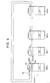
- each entry has a pointer Pa as the first field thereof including an address indicating the first address of an entry following the entry, thereby constructing a sequence of data array by linking the entries with the pointers.
- a queue having a double link structure namely, each entry is provided with a pointer Pb following the pointer field Pa so as to indicate a backward linkage of the entry.
- the queue configured in this fashion is used in a case where, for example, each entry is used to store jobs (or tasks) requested from a plurality of users and an entry satisfying a predetermined condition is selected from the entries for an execution.
- a new retrieval instruction is added to retrieve a queue and the queue retrieval instruction is effected after data necessary for the queue retrieval such as the first address of the first entry, a compare value as a condition for the selection, and an offset value of the retrieval data in the entry are set to predetermined registers.
- the first address of a desired entry is obtained by the queue retrieval instruction and by a register set instruction preceding the queue retrieval instruction so as to increase the queue retrieval speed, which enables to achieve the object that the efficiency of the operating system handing the multitask, multiuser processing, and the like is improved.
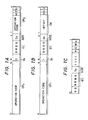
- FIG. 1A shows an embodiment of an instruction format of a queue retrieval instruction (to be referred to as a queue search instruction herebelow) in a case where the present invention is applied to a microprocessor having an instruction system in which the instruction configuration unit is 16 or 32 bits.
- the queue search instruction shown in FIG. 1A includes operation designation fields OP 1 and OP z respectively containing 16 high-order bits and 8 low-order bits each representing operation codes, an end condition designation field EC designating an end condition of the instruction, a size designation field Sz indicating the magnitude of the compare value, a format bit field Bi designating the format of the instruction, an M bit field indicating the presence or absence of a mask of R 6 , an E bit indicating the end value of the queue, and a U bit designating the direction of the search operation.
- FIG. 1B shows a second format of the queue search instruction according to the present invention.
- the second instruction format is different from the first instruction format (FIG. 1A) in a point that an immediate addressing is adopted for the offset value. Namely, in the second instruction format, the 5 low-order bits of the 7 bits constituting the operation designation field OP 2 in the first instruction formation are replaced with the immediate field IM.
- the discrimination between the first format and the second format is effected by use of the bit Bii, for example, if the bit Bi is "0", the 5 low-order bits of the instruction word is treated as the operation designation field OP t ; whereas if the bit Bi is "1", the 5 low-order bits of the instruction word is treated as the immediate field IM.
- the immediate field IM comprises five bits, the 5-bit code of the immediate field must be converted into a 32-bit wide data by use of a sign expansion, or the like.
- the end condition designation field EC includes four bits, which are defined, for example, as listed in Table 1 as follows.
- End conditions No.1 to No.5 represent the cases where the end conditions are established according to the comparison between the data read from an entry with the value in the register R a
- the end conditions No.6 to No.9 denote the cases where the end conditions are set depending on the comparison between the value of the register R 3 and that of the register R 4 .
- the size designation field Sz is constituted from two bits and, for example, if the two bits are "00", the compare value includes eight bits; if the two bits are "01”, the compare value includes 16 bits; and if the two bits are "10", the compare value includes 32 bits. Consequently, in a case where the compare value is beforehand loaded in a register (32 bits) as will be described later, the system operates according to the contents of the size designation field Sz to handle information of the 8, 16, or 32 low-order bits as the effective compare value.
- the M bit when the M bit is "0", it is indicated that the mask of the register R a is absent; whereas, when the M bit is "1", the mask is indicated to be present.
- the arrangement of the respective fields in the 32-bit area does not possess any substantial meaning.
- the 32-bit queue search instruction is split into two words so as to be read in an instruction register through two 16-bit read operations.
- FIG. 1C is a schematic diagram illustrating another embodiment of the queue search instruction according to the present invention.
- This queue search instruction comprises 16 bits.
- the operation designation fields OP,, OP 2 , and OP3 are used to specify that this instruction is a queue search instruction.
- the instruction format includes the M bit, the U bit, and the like.
- An offset value necessary for an execution of this instruction is beforehand set to, for example, the register R 5 .
- FIG. 2 there is shown a processing flowchart of a microprogram in a microprocessor to decode and to execute the queue search instructio.
- the first address of the search start entry, the compare value, and the offset value (unnecessary in the second instruction format) required for the queue retrieval are beforehand loaded in predetermined general-purpose registers, for example, R 1 , R 3 , and R 5 , respectively for an execution of the queue search instruction.
- the status register in the microprocessor is provided with a flag (to be referred to as an F flag herebelow) indicating whether or not the retrieval has been completed. If the F flag is "0", the retrieval is indicated to have been successfully completed; whereas if the F flag is "1", the entry to be retrieved is indicated to be missing.
- step Si the first address of the starting entry in the register R o is set as a copy to a temporary register TEMP (which cannot be accessed by the user).
- step S2 the memory is accessed by use of an address obtained by adding the offset value in the register R S or the immediate field to the address in the register R 0 so as to read data, which is then compared with the search data (compare value) in the register R 3 , thereby judging whether or not the specified condition (Table 1) is satisfied.
- the end condition BBBB is indicated to be 000i. That is, assuming the entry ENT 0 to be the search start entry in FIG.
- an access is made at a position of an address obtained by adding the offset value OF to the first address A of the entry ENT o to read data Key stored therein and a judgement is effected to determine whether or not the data Key is matched with the search data in the register R 3 .
- step S2 results in Yes (equal to)
- control is passed to step S7 to clear the F flag to 0, thereby terminating the instruction. That is, a fact that the data Key read in the step S2 is matched with the search data (compare value) indicates that the address in the register R o is the first address of the entry to be obtained and hence the retrieval can be terminated with the address kept remained in the register R o .
- the instruction is terminated with the address A o stored in the register R o .
- step S3 the code of the bit U is judged to be equal to "0" or not. If the bit U is "1”, step S4 is effected to access the memory at an address obtained by adding "4" at the address in the register R o so as to obtain data and to store the obtained data in the register R o .
- the position obtained by adding "4" to the entry start address in the register R o indicates the pointer Pb in which the first address of the next entry is stored in a search in the backward direction in FIG. 4.
- step S5 control is passed to step S5 and the address contained in the register R o is used to access the memory so as to store data in the register R o . That is, in FIG. 4, the first address of the next entry indicated by the forward-directional pointer Pa of the entry for which the retrieval has been just finished is stored in the register R o .
- step S6 to compare the value in the register Ro at the point with the value in the temporary register TEMP into which the value of R 0 has been loaded in the step S1, thereby judging whether or not these values match with each other. If the values does not match with each other, control returns to the step S2 to repeat the procedure described above; otherwise, control is passed to step S8 to set "1" to the F flag, thereby terminating the processing. That is, a fact that the values of these registers match with each other in the step S6 means that the position of the entry to be retrieved in FIG. 4 is returned to the entry from which the retrieval was started, namely, an objective entry has not been found by the retrieval operation through the queue. The processing thus terminates the operation thereof by indicating that the retrieval is unsuccessful.
- the address stored in the register R o at the point is the first address of the objective entry; thereafter, by reading data in the associated entry based on the address in the register R o , the multitask processing, multiuser processing, and the like can be smoothly effected.
- the queue search can be executed by use of an instruction on assumption that the registers R 0 . R 3 , and R 5 beforehand contain the first address of the search start entry, the compare value, and the offset value, respectively. Consequently, comparing with a method in which the retrieval is effected by use of, for example, a MOVE instruction when the queue search instruction is not provided, the efficiency of the operating system of this method is considerably improved; furthermore, the period of time required to retrieve the entry is minimized.
- the microprocessor of the embodiment above is also provided with instructions to insert, to delete, and to replace entries.
- FIG. 3 is a schematic block diagram illustrating an example of the hardware configuration of the microprocessor operating by use of an instruction system having the queue search instruction according to the present invention.
- the microprocessor of this embodiment includes a control section operating under control of microprograms. That is, in an LSI chip 1 constituting the microprocessor, there is disposed a micro (read only memory) ROM 2, which is accessed by a micro address generator circuit 5 and sequentially outputs micro instructions contained in the microprograms.
- a micro (read only memory) ROM 2 which is accessed by a micro address generator circuit 5 and sequentially outputs micro instructions contained in the microprograms.
- the micro address generator circuit 5 is supplied with a signal obtained by decoding in an instruction decoder 4 a code of a macro instruction fetched by an instruction register 3. Based on the supplied signal, the micro address generator circuit 5 forms the corresponding micro address and supplies the address to the micro ROM 2, which causes to read the first micro instruction of a series of micro instruction groups executing the macro instruction. Based on the micro instruction code, the system generates control signals for components such as an execution unit 6 having various temporary registers, data buffers, an arithmetic logic unit (ALU), an address calculation unit (AU), and the like.
- ALU arithmetic logic unit
- AU address calculation unit
- the read operations of the second and subsequent micro instructions in the sequence of micro instruction groups corresponding to the macro instruction are effected by supplying the micro ROM 2 with the code of the next address field of the micro instruction previously read. That is, there is provided a micro instruction latch 9 for keeping the next address in the previous micro instruction, and the read operations of the second and subsequent micro instructions are achieved based on an output from the micro instruction latch 9 and an address from the micro address generator circuit 5.
- a sequence of micro instructions thus read are decoded by a micro instruction decoder 10, which outputs a control signal to control the execution unit 6, thereby executing the macro instruction.
- the address calculation unit (AU) calculates an address of the memory based on information such as an offset value.
- the buffer store method is adopted, namely, a cache memory 7 is disposed in the microprocessor LSI so as to register to the cache memory 7 the program data to be frequently used among the data stored in an external memory 8. This enables to increase the speed to fetch a program.
- FIGS. 5A-5C are flowcharts of another embodiment according to the queue search instruction of the present invention.
- the instruction When the instruction is to be executed, information necessary for the queue retrieval is beforehand written in predetermined registers in the microprocessor. That is, the registers R 2 , R 3 , R 4 , R s , and R6 are loaded with the first address of the search end entry, the first compare value, the second compare value, the offset value, and data for the mask, respectively.
- the data for the mask is data used to assign a meaning of data to predetermined bits among a plurality of bits constituting a data item.
- two registers R 0 and R 1 are disposed to set the first addresses of entries.
- the first address of the entry being searched for is set to the register R o
- the first address of the entry immediately preceding the entry being searched for is set to the register R 1 .
- the status register in the microprocessor is provided with a flag F and a flag V.
- the flag F is used to indicate the result of the retrieval using the first compare value in the register R 3
- the flag V is disposed to indicate the result of the retrieval using the second compare value in the register R 4 .
- step ST1 it is judged whether or not an interrupt request exits. If this is the case, the interrupt request takes precedence and therefore the queue search instruction is terminated; otherwise, control is passed to step ST2.
- step ST2 the content of the register R o is set to the register R 1 , which updates the content of the register R l .
- step ST4 the memory is accessed to obain data by use of an address obatined by adding 4 to the address in the register R l and the obtained data is loaded in the register R o .
- the step ST4 or ST9 sets the first address of the entry to be retrieved to the register R o .
- step ST5 it is judged whether or not the content of the register R 0 matches with that of the register R2. If the contents match with each other, it is indicated that the entry to be retrieved reaches the position of the search end entry; consequently, "1" is set to the flag F (step ST 10) and the search instruction is terminated.
- step ST6 If the contents do not match with each other, control is passed to the step ST6, where it is judged whether or not the mask is necesssary for the data to be used for the retrieval.
- step ST8 the memory is accessed to obtain data by use of an address calculated by adding the offset value in the register R, to the address in the regsiter R o and the the data is compared with the compare value in the register R1, thereby judging whether or not the specified condition (Table 1) is satisfied.
- the end condition BBBB is indicated to be 0001. That is, in FIG. 4, assuming the entry ENT O to be the search start entry, the memory is accessed by use of an address obtained by adding the offset value OF to the first address A of the entry ENTo so as to read data Key at the resultant address, and then it is judged whether or not the data Key matches with the search data in the register R 3 .
- step ST8 results in Yes (equal to)
- control is passed to step ST11 and the flag F is cleared to "0", thereby terminating the instruction.
- a fact that the data Key read in the step ST8 matches with the search data (compare value) means that the address in the register R o at the point is the first address of the objective entry; consequently, the retrieval can be terminated with the address kept remained in the register R 0 .
- the processing is terminated with the address A o kept stored in the register R o . If the step ST8 results in No (not equal to), control returns to the step ST1.
- step ST17 the memory is accessed to attain data by use of an address calculated by adding the offset value in the register R 5 to the address in the register R o , and then the data is compared with the first compare value in the register R 3 for the judgement.
- the data is greater than the first compare value, one of the end conditions is satisfied; consequently, "0" is set to the flag F (step ST20) and then control is passed to step ST18. If the data is equal to or less than the first compare value, the end condition is not satisfied; consequently, the program proceeds to step ST18 with the flag F kept set to the initial value, "1".
- step ST18 the data is compared with the second compare value in the register R 4 for the judgement.
- the data is less than the second compare value, one of the end conditions is satisfied; consequently, "0" is set to the flag V (step ST21) and then control is passed to step ST19.
- the program proceeds to step ST19 with the flag F kept set to the initial value, "I”.
- step ST6 of FIG. 5A results in Yes.
- step ST1 2 like in the step ST7 of FIG. 5A, it is judged whether or not the content of the register R 4 is necessary in judging the retrieval end condition. In a case where the content of the register R4 is necessary, the flow is basically the same as that of FIG. 5C; consequently, description thereof will be omitted. If the content of the register R 4 is not required, control is passed to step ST13, where the memory is accessed to attain data by use of an address calculated by adding the offset value in the register R 5 to the address in the register R o and the data is masked with the content of the register R 6 .
- step ST14 the compare value in the register R 3 and the content of the register R 6 are ANDed and the result is set to the register R a .
- step ST15 the content of the register R 7 is compared with the content of the register R 8 to judge whether or not the specified conditions (Table 1) are satisfied. In this embodiment, the end condition BBBB is indicated to be 0001. If the step ST15 results in Yes in the judgement, control is passed to the step ST16, where the flag F is cleared to 0, thereby terminating the instruction. If the step ST15 results in No, control returns to the step ST1.
- a new instruction to retrieve a queue is added and the queue retrieval instruction is executed after the first address of the retrieval start entry, the compare value as the selection condition, and tne offset value of the retrieval data in an entry each necessary for the queue retrieval are beforehand loaded in predetermined registers; consequently, the first address of the desired entry can be attained by a queue retrieval instruction and a register setting instruction preceding the queue retrieval instruction, which increases the speed of the queue retrieval and which enables to obtain an effect that the efficiency of the operating system handling the multitask processing, the multiuser processing, and the like is improved.
- the queue search is executed with an instruction on assumption that the registers R 0 , R J , and R S are beforehand loaded with the first address of the search start entry, the compare value, and the offset value, respectively, the data items such as the first address need not be set to the regsiters by use of instructions, namely, the data items may be supplied as operands of the queue search instruction.
- the queue retrieval speed is increased and hence the efficiency of the operating system handling the multitask processing, the multiuser processing, and the like can be improved.
Landscapes
- Engineering & Computer Science (AREA)
- Theoretical Computer Science (AREA)
- Software Systems (AREA)
- Physics & Mathematics (AREA)
- General Engineering & Computer Science (AREA)
- General Physics & Mathematics (AREA)
- Databases & Information Systems (AREA)
- Data Mining & Analysis (AREA)
- Executing Machine-Instructions (AREA)
- Microcomputers (AREA)
- Information Retrieval, Db Structures And Fs Structures Therefor (AREA)
Applications Claiming Priority (2)
| Application Number | Priority Date | Filing Date | Title |
|---|---|---|---|
| JP198869/86 | 1986-08-27 | ||
| JP61198869A JPS6355636A (ja) | 1986-08-27 | 1986-08-27 | デ−タ処理システム |
Publications (2)
| Publication Number | Publication Date |
|---|---|
| EP0257252A2 true EP0257252A2 (de) | 1988-03-02 |
| EP0257252A3 EP0257252A3 (de) | 1991-01-16 |
Family
ID=16398276
Family Applications (1)
| Application Number | Title | Priority Date | Filing Date |
|---|---|---|---|
| EP19870109718 Withdrawn EP0257252A3 (de) | 1986-08-27 | 1987-07-06 | Mikroprozessor |
Country Status (4)
| Country | Link |
|---|---|
| US (2) | US4926321A (de) |
| EP (1) | EP0257252A3 (de) |
| JP (1) | JPS6355636A (de) |
| KR (1) | KR950006587B1 (de) |
Families Citing this family (7)
| Publication number | Priority date | Publication date | Assignee | Title |
|---|---|---|---|---|
| US5170474A (en) * | 1986-08-27 | 1992-12-08 | Hitachi, Ltd. | Method of searching a queue in response to a search instruction |
| JPS6355636A (ja) * | 1986-08-27 | 1988-03-10 | Hitachi Ltd | デ−タ処理システム |
| GB2228597A (en) * | 1989-02-27 | 1990-08-29 | Ibm | Data processor with conditional instructions |
| JP4856444B2 (ja) * | 2005-03-07 | 2012-01-18 | 株式会社リコー | 情報処理装置及び情報処理方法 |
| CN103187104B (zh) * | 2013-03-19 | 2016-11-23 | 西安紫光国芯半导体有限公司 | Dram存储器的纠错方法 |
| CN103294797B (zh) * | 2013-05-24 | 2016-06-22 | 中国人民解放军信息工程大学 | 基于相容优化的并行约束求解方法 |
| KR102901778B1 (ko) * | 2020-03-25 | 2025-12-19 | 에스케이하이닉스 주식회사 | 메모리 컨트롤러 및 그 동작 방법 |
Family Cites Families (14)
| Publication number | Priority date | Publication date | Assignee | Title |
|---|---|---|---|---|
| US3821708A (en) * | 1969-05-20 | 1974-06-28 | B Sokoloff | Electronic control unit for the linking of symmetrical closed chains of words in a random access memory |
| JPS6020767B2 (ja) * | 1975-06-24 | 1985-05-23 | 日本電気株式会社 | 情報探索機能を有する電子計算機 |
| US4245304A (en) * | 1978-12-11 | 1981-01-13 | Honeywell Information Systems Inc. | Cache arrangement utilizing a split cycle mode of operation |
| US4384343A (en) * | 1979-02-12 | 1983-05-17 | Honeywell Information Systems Inc. | Firmware controlled search and verify apparatus and method for a data processing system |
| US4535420A (en) * | 1979-09-26 | 1985-08-13 | Sperry Corporation | Circular-queue structure |
| US4481608A (en) * | 1979-12-26 | 1984-11-06 | Varian Associates, Inc. | Reentrant asynchronous FIFO |
| US4358829A (en) * | 1980-04-14 | 1982-11-09 | Sperry Corporation | Dynamic rank ordered scheduling mechanism |
| JPS5941064A (ja) * | 1982-08-31 | 1984-03-07 | Nec Corp | プロログ処理装置 |
| US4482956A (en) * | 1982-11-04 | 1984-11-13 | International Business Machines Corporation | Parallel queueing method |
| US4701847A (en) * | 1985-01-09 | 1987-10-20 | Logical Services, Inc. | Adaptive instruction sequence synthesizer and process |
| JPS6298434A (ja) * | 1985-10-25 | 1987-05-07 | Hitachi Ltd | デ−タ処理システム |
| JPS6355636A (ja) * | 1986-08-27 | 1988-03-10 | Hitachi Ltd | デ−タ処理システム |
| US4992938A (en) * | 1987-07-01 | 1991-02-12 | International Business Machines Corporation | Instruction control mechanism for a computing system with register renaming, map table and queues indicating available registers |
| US5008816A (en) * | 1987-11-06 | 1991-04-16 | International Business Machines Corporation | Data processing system with multi-access memory |
-
1986
- 1986-08-27 JP JP61198869A patent/JPS6355636A/ja active Pending
-
1987
- 1987-07-06 EP EP19870109718 patent/EP0257252A3/de not_active Withdrawn
- 1987-07-18 KR KR1019870007806A patent/KR950006587B1/ko not_active Expired - Lifetime
- 1987-08-27 US US07/089,818 patent/US4926321A/en not_active Expired - Lifetime
-
1990
- 1990-03-26 US US07/489,240 patent/US5073856A/en not_active Expired - Fee Related
Also Published As
| Publication number | Publication date |
|---|---|
| US5073856A (en) | 1991-12-17 |
| KR880003240A (ko) | 1988-05-14 |
| JPS6355636A (ja) | 1988-03-10 |
| KR950006587B1 (ko) | 1995-06-19 |
| EP0257252A3 (de) | 1991-01-16 |
| US4926321A (en) | 1990-05-15 |
Similar Documents
| Publication | Publication Date | Title |
|---|---|---|
| EP0220684B1 (de) | Datenverarbeitungssystem | |
| US4454578A (en) | Data processing unit with pipelined operands | |
| US4679140A (en) | Data processor with control of the significant bit lengths of general purpose registers | |
| US5276891A (en) | Alignment of sign, data, edit byte operand results for storage in memory | |
| EP0471191B1 (de) | Datenprozessor mit der Fähigkeit, zwei Befehle gleichzeitig auszuführen | |
| USRE32493E (en) | Data processing unit with pipelined operands | |
| US4833640A (en) | Register bank change including register to register transfer in a data processing system | |
| US6338134B1 (en) | Method and system in a superscalar data processing system for the efficient processing of an instruction by moving only pointers to data | |
| EP0465248A2 (de) | Speichererweiterungsschema mit pseudo-linearer Bankumschaltung für einen Mikrokontroller | |
| EP0315139B1 (de) | Mikroprozessor | |
| US20030028754A1 (en) | Data processor using indirect register addressing | |
| US4933847A (en) | Microcode branch based upon operand length and alignment | |
| EP1003094B1 (de) | Zentrale Verarbeitungseinheit mit Befehl zur Datenverlängerung | |
| EP0257252A2 (de) | Mikroprozessor | |
| US4764869A (en) | Method and apparatus for controlling interruption in the course of instruction execution in a processor | |
| US5170474A (en) | Method of searching a queue in response to a search instruction | |
| US7546442B1 (en) | Fixed length memory to memory arithmetic and architecture for direct memory access using fixed length instructions | |
| US5077659A (en) | Data processor employing the same microprograms for data having different bit lengths | |
| JPH07239780A (ja) | 1クロック可変長命令実行処理型命令読み込み電子計 算機 | |
| US4611278A (en) | Wraparound buffer for repetitive decimal numeric operations | |
| US20030046516A1 (en) | Method and apparatus for extending instructions with extension data of an extension register | |
| EP0361107A2 (de) | Mikroprogrammgesteuerter Mikroprozessor mit Zeiger-Register und Zugriffsverfahren dafür | |
| US5991870A (en) | Processor for executing an instructions stream where instruction have both a compressed and an uncompressed register field | |
| US5390306A (en) | Pipeline processing system and microprocessor using the system | |
| EP0382235A2 (de) | Mikroprogramm-Steuervorrichtung |
Legal Events
| Date | Code | Title | Description |
|---|---|---|---|
| PUAI | Public reference made under article 153(3) epc to a published international application that has entered the european phase |
Free format text: ORIGINAL CODE: 0009012 |
|
| AK | Designated contracting states |
Kind code of ref document: A2 Designated state(s): DE FR GB IT |
|
| PUAL | Search report despatched |
Free format text: ORIGINAL CODE: 0009013 |
|
| AK | Designated contracting states |
Kind code of ref document: A3 Designated state(s): DE FR GB IT |
|
| RHK1 | Main classification (correction) |
Ipc: G06F 15/40 |
|
| 17P | Request for examination filed |
Effective date: 19901212 |
|
| RAP1 | Party data changed (applicant data changed or rights of an application transferred) |
Owner name: SAKAMURA, KEN Owner name: HITACHI, LTD. Owner name: HITACHI MICROCOMPUTER SYSTEM LTD. |
|
| 17Q | First examination report despatched |
Effective date: 19920302 |
|
| STAA | Information on the status of an ep patent application or granted ep patent |
Free format text: STATUS: THE APPLICATION IS DEEMED TO BE WITHDRAWN |
|
| 18D | Application deemed to be withdrawn |
Effective date: 19940607 |
|
| RIN1 | Information on inventor provided before grant (corrected) |
Inventor name: KAWASAKI, IKUYA Inventor name: SAKAMURA, KEN Inventor name: HASEGAWA, ATSUSHI Inventor name: IWASAKI, KAZUHIKO Inventor name: HASHIMOTO, KOUZI |