EP0257638A2 - Vorrichtung zur optischen Modulation - Google Patents
Vorrichtung zur optischen Modulation Download PDFInfo
- Publication number
- EP0257638A2 EP0257638A2 EP87112410A EP87112410A EP0257638A2 EP 0257638 A2 EP0257638 A2 EP 0257638A2 EP 87112410 A EP87112410 A EP 87112410A EP 87112410 A EP87112410 A EP 87112410A EP 0257638 A2 EP0257638 A2 EP 0257638A2
- Authority
- EP
- European Patent Office
- Prior art keywords
- liquid crystal
- voltage
- ferroelectric liquid
- electrodes
- disposed
- Prior art date
- Legal status (The legal status is an assumption and is not a legal conclusion. Google has not performed a legal analysis and makes no representation as to the accuracy of the status listed.)
- Granted
Links
- 230000003287 optical effect Effects 0.000 title claims abstract description 40
- 239000005262 ferroelectric liquid crystals (FLCs) Substances 0.000 claims abstract description 31
- 239000000758 substrate Substances 0.000 claims abstract description 15
- 239000004990 Smectic liquid crystal Substances 0.000 claims description 10
- 239000011159 matrix material Substances 0.000 claims description 2
- 239000004020 conductor Substances 0.000 claims 6
- 238000002834 transmittance Methods 0.000 abstract description 13
- 239000004973 liquid crystal related substance Substances 0.000 description 23
- 210000004027 cell Anatomy 0.000 description 10
- 210000002858 crystal cell Anatomy 0.000 description 10
- 230000005684 electric field Effects 0.000 description 7
- 239000011521 glass Substances 0.000 description 5
- 230000004044 response Effects 0.000 description 5
- 230000000875 corresponding effect Effects 0.000 description 3
- 238000010586 diagram Methods 0.000 description 3
- 230000000694 effects Effects 0.000 description 3
- VYPSYNLAJGMNEJ-UHFFFAOYSA-N Silicium dioxide Chemical compound O=[Si]=O VYPSYNLAJGMNEJ-UHFFFAOYSA-N 0.000 description 2
- 150000001875 compounds Chemical class 0.000 description 2
- 230000003247 decreasing effect Effects 0.000 description 2
- 238000007740 vapor deposition Methods 0.000 description 2
- RYGMFSIKBFXOCR-UHFFFAOYSA-N Copper Chemical compound [Cu] RYGMFSIKBFXOCR-UHFFFAOYSA-N 0.000 description 1
- 239000004988 Nematic liquid crystal Substances 0.000 description 1
- XUIMIQQOPSSXEZ-UHFFFAOYSA-N Silicon Chemical compound [Si] XUIMIQQOPSSXEZ-UHFFFAOYSA-N 0.000 description 1
- XAGFODPZIPBFFR-UHFFFAOYSA-N aluminium Chemical compound [Al] XAGFODPZIPBFFR-UHFFFAOYSA-N 0.000 description 1
- 229910052782 aluminium Inorganic materials 0.000 description 1
- 229910021417 amorphous silicon Inorganic materials 0.000 description 1
- 238000013459 approach Methods 0.000 description 1
- 230000005540 biological transmission Effects 0.000 description 1
- 239000003990 capacitor Substances 0.000 description 1
- 238000006243 chemical reaction Methods 0.000 description 1
- 229940114081 cinnamate Drugs 0.000 description 1
- 229910052681 coesite Inorganic materials 0.000 description 1
- 238000010276 construction Methods 0.000 description 1
- 230000001276 controlling effect Effects 0.000 description 1
- 229910052802 copper Inorganic materials 0.000 description 1
- 239000010949 copper Substances 0.000 description 1
- 229910052906 cristobalite Inorganic materials 0.000 description 1
- 239000000463 material Substances 0.000 description 1
- 239000000203 mixture Substances 0.000 description 1
- 230000003334 potential effect Effects 0.000 description 1
- 230000000717 retained effect Effects 0.000 description 1
- 229920006395 saturated elastomer Polymers 0.000 description 1
- 229910052710 silicon Inorganic materials 0.000 description 1
- 239000010703 silicon Substances 0.000 description 1
- 239000000377 silicon dioxide Substances 0.000 description 1
- 235000012239 silicon dioxide Nutrition 0.000 description 1
- 239000007787 solid Substances 0.000 description 1
- 229910052682 stishovite Inorganic materials 0.000 description 1
- 230000007704 transition Effects 0.000 description 1
- 229910052905 tridymite Inorganic materials 0.000 description 1
- 230000000007 visual effect Effects 0.000 description 1
Images


Classifications
-
- G—PHYSICS
- G09—EDUCATION; CRYPTOGRAPHY; DISPLAY; ADVERTISING; SEALS
- G09G—ARRANGEMENTS OR CIRCUITS FOR CONTROL OF INDICATING DEVICES USING STATIC MEANS TO PRESENT VARIABLE INFORMATION
- G09G3/00—Control arrangements or circuits, of interest only in connection with visual indicators other than cathode-ray tubes
- G09G3/20—Control arrangements or circuits, of interest only in connection with visual indicators other than cathode-ray tubes for presentation of an assembly of a number of characters, e.g. a page, by composing the assembly by combination of individual elements arranged in a matrix no fixed position being assigned to or needed to be assigned to the individual characters or partial characters
- G09G3/34—Control arrangements or circuits, of interest only in connection with visual indicators other than cathode-ray tubes for presentation of an assembly of a number of characters, e.g. a page, by composing the assembly by combination of individual elements arranged in a matrix no fixed position being assigned to or needed to be assigned to the individual characters or partial characters by control of light from an independent source
- G09G3/36—Control arrangements or circuits, of interest only in connection with visual indicators other than cathode-ray tubes for presentation of an assembly of a number of characters, e.g. a page, by composing the assembly by combination of individual elements arranged in a matrix no fixed position being assigned to or needed to be assigned to the individual characters or partial characters by control of light from an independent source using liquid crystals
- G09G3/3611—Control of matrices with row and column drivers
- G09G3/3622—Control of matrices with row and column drivers using a passive matrix
- G09G3/3629—Control of matrices with row and column drivers using a passive matrix using liquid crystals having memory effects, e.g. ferroelectric liquid crystals
-
- G—PHYSICS
- G02—OPTICS
- G02F—OPTICAL DEVICES OR ARRANGEMENTS FOR THE CONTROL OF LIGHT BY MODIFICATION OF THE OPTICAL PROPERTIES OF THE MEDIA OF THE ELEMENTS INVOLVED THEREIN; NON-LINEAR OPTICS; FREQUENCY-CHANGING OF LIGHT; OPTICAL LOGIC ELEMENTS; OPTICAL ANALOGUE/DIGITAL CONVERTERS
- G02F1/00—Devices or arrangements for the control of the intensity, colour, phase, polarisation or direction of light arriving from an independent light source, e.g. switching, gating or modulating; Non-linear optics
- G02F1/01—Devices or arrangements for the control of the intensity, colour, phase, polarisation or direction of light arriving from an independent light source, e.g. switching, gating or modulating; Non-linear optics for the control of the intensity, phase, polarisation or colour
- G02F1/13—Devices or arrangements for the control of the intensity, colour, phase, polarisation or direction of light arriving from an independent light source, e.g. switching, gating or modulating; Non-linear optics for the control of the intensity, phase, polarisation or colour based on liquid crystals, e.g. single liquid crystal display cells
- G02F1/137—Devices or arrangements for the control of the intensity, colour, phase, polarisation or direction of light arriving from an independent light source, e.g. switching, gating or modulating; Non-linear optics for the control of the intensity, phase, polarisation or colour based on liquid crystals, e.g. single liquid crystal display cells characterised by the electro-optical or magneto-optical effect, e.g. field-induced phase transition, orientation effect, guest-host interaction or dynamic scattering
- G02F1/139—Devices or arrangements for the control of the intensity, colour, phase, polarisation or direction of light arriving from an independent light source, e.g. switching, gating or modulating; Non-linear optics for the control of the intensity, phase, polarisation or colour based on liquid crystals, e.g. single liquid crystal display cells characterised by the electro-optical or magneto-optical effect, e.g. field-induced phase transition, orientation effect, guest-host interaction or dynamic scattering based on orientation effects in which the liquid crystal remains transparent
- G02F1/141—Devices or arrangements for the control of the intensity, colour, phase, polarisation or direction of light arriving from an independent light source, e.g. switching, gating or modulating; Non-linear optics for the control of the intensity, phase, polarisation or colour based on liquid crystals, e.g. single liquid crystal display cells characterised by the electro-optical or magneto-optical effect, e.g. field-induced phase transition, orientation effect, guest-host interaction or dynamic scattering based on orientation effects in which the liquid crystal remains transparent using ferroelectric liquid crystals
-
- G—PHYSICS
- G02—OPTICS
- G02F—OPTICAL DEVICES OR ARRANGEMENTS FOR THE CONTROL OF LIGHT BY MODIFICATION OF THE OPTICAL PROPERTIES OF THE MEDIA OF THE ELEMENTS INVOLVED THEREIN; NON-LINEAR OPTICS; FREQUENCY-CHANGING OF LIGHT; OPTICAL LOGIC ELEMENTS; OPTICAL ANALOGUE/DIGITAL CONVERTERS
- G02F1/00—Devices or arrangements for the control of the intensity, colour, phase, polarisation or direction of light arriving from an independent light source, e.g. switching, gating or modulating; Non-linear optics
- G02F1/01—Devices or arrangements for the control of the intensity, colour, phase, polarisation or direction of light arriving from an independent light source, e.g. switching, gating or modulating; Non-linear optics for the control of the intensity, phase, polarisation or colour
- G02F1/13—Devices or arrangements for the control of the intensity, colour, phase, polarisation or direction of light arriving from an independent light source, e.g. switching, gating or modulating; Non-linear optics for the control of the intensity, phase, polarisation or colour based on liquid crystals, e.g. single liquid crystal display cells
- G02F1/133—Constructional arrangements; Operation of liquid crystal cells; Circuit arrangements
- G02F1/13306—Circuit arrangements or driving methods for the control of single liquid crystal cells
-
- G—PHYSICS
- G02—OPTICS
- G02F—OPTICAL DEVICES OR ARRANGEMENTS FOR THE CONTROL OF LIGHT BY MODIFICATION OF THE OPTICAL PROPERTIES OF THE MEDIA OF THE ELEMENTS INVOLVED THEREIN; NON-LINEAR OPTICS; FREQUENCY-CHANGING OF LIGHT; OPTICAL LOGIC ELEMENTS; OPTICAL ANALOGUE/DIGITAL CONVERTERS
- G02F1/00—Devices or arrangements for the control of the intensity, colour, phase, polarisation or direction of light arriving from an independent light source, e.g. switching, gating or modulating; Non-linear optics
- G02F1/01—Devices or arrangements for the control of the intensity, colour, phase, polarisation or direction of light arriving from an independent light source, e.g. switching, gating or modulating; Non-linear optics for the control of the intensity, phase, polarisation or colour
- G02F1/13—Devices or arrangements for the control of the intensity, colour, phase, polarisation or direction of light arriving from an independent light source, e.g. switching, gating or modulating; Non-linear optics for the control of the intensity, phase, polarisation or colour based on liquid crystals, e.g. single liquid crystal display cells
- G02F1/137—Devices or arrangements for the control of the intensity, colour, phase, polarisation or direction of light arriving from an independent light source, e.g. switching, gating or modulating; Non-linear optics for the control of the intensity, phase, polarisation or colour based on liquid crystals, e.g. single liquid crystal display cells characterised by the electro-optical or magneto-optical effect, e.g. field-induced phase transition, orientation effect, guest-host interaction or dynamic scattering
- G02F1/13756—Devices or arrangements for the control of the intensity, colour, phase, polarisation or direction of light arriving from an independent light source, e.g. switching, gating or modulating; Non-linear optics for the control of the intensity, phase, polarisation or colour based on liquid crystals, e.g. single liquid crystal display cells characterised by the electro-optical or magneto-optical effect, e.g. field-induced phase transition, orientation effect, guest-host interaction or dynamic scattering the liquid crystal selectively assuming a light-scattering state
-
- G—PHYSICS
- G09—EDUCATION; CRYPTOGRAPHY; DISPLAY; ADVERTISING; SEALS
- G09G—ARRANGEMENTS OR CIRCUITS FOR CONTROL OF INDICATING DEVICES USING STATIC MEANS TO PRESENT VARIABLE INFORMATION
- G09G2310/00—Command of the display device
- G09G2310/06—Details of flat display driving waveforms
-
- G—PHYSICS
- G09—EDUCATION; CRYPTOGRAPHY; DISPLAY; ADVERTISING; SEALS
- G09G—ARRANGEMENTS OR CIRCUITS FOR CONTROL OF INDICATING DEVICES USING STATIC MEANS TO PRESENT VARIABLE INFORMATION
- G09G2320/00—Control of display operating conditions
- G09G2320/02—Improving the quality of display appearance
- G09G2320/0209—Crosstalk reduction, i.e. to reduce direct or indirect influences of signals directed to a certain pixel of the displayed image on other pixels of said image, inclusive of influences affecting pixels in different frames or fields or sub-images which constitute a same image, e.g. left and right images of a stereoscopic display
-
- G—PHYSICS
- G09—EDUCATION; CRYPTOGRAPHY; DISPLAY; ADVERTISING; SEALS
- G09G—ARRANGEMENTS OR CIRCUITS FOR CONTROL OF INDICATING DEVICES USING STATIC MEANS TO PRESENT VARIABLE INFORMATION
- G09G3/00—Control arrangements or circuits, of interest only in connection with visual indicators other than cathode-ray tubes
- G09G3/20—Control arrangements or circuits, of interest only in connection with visual indicators other than cathode-ray tubes for presentation of an assembly of a number of characters, e.g. a page, by composing the assembly by combination of individual elements arranged in a matrix no fixed position being assigned to or needed to be assigned to the individual characters or partial characters
- G09G3/2007—Display of intermediate tones
- G09G3/2011—Display of intermediate tones by amplitude modulation
Definitions
- the present invention relates to an optical modulation device applicable to a display panel, an optical shutter array, etc., particularly an optical modulation device using a ferroelectric liquid crystal.
- a copy formed by such an electrophotographic printer has an image with two density levels of ordinarily "white” and "black".
- Clark et al have disclosed a chiral smectic liquid crystal device provided with a memory characteristic in U.S. Patent Nos. 4,367,924 and 4,563,059.
- the chiral smectic liquid crystal device is known to form a first stable orientation state corresponding to, e.g., "while” of the two levels and a second stable orientation state corresponding to "black” in response to the direction of an electric field applied. Accordingly, the chiral smectic liquid crystal device causes rapid transition from white (or black) to black (or white) in response to application of voltages with different polarities so that it involves a problem that gradational display by voltage amplitude control is difficult particularly under high speed driving.
- an electrophotographic printer is required of high speed driving more and more. For this reason, it becomes further more difficult to apply the above-mentioned chiral smectic liquid crystal device to a shutter array element for an electrophotographic printer to obtain a copy image with gradation.
- U.S. Patent No. 3,675,988 discloses a nematic liquid crystal device wherein one display region is allowed to have white and black regions in a controlled ratio, but the device is not used for providing a gradational image.
- M. Geary, SID DIGEST (1985) p. 128 discloses application of an AC voltage to a ferroelectric liquid crystal, but the application of the AC voltage is effected for bistabilization of the ferroelectric liquid crystal cell and not for providing a gradation.
- an object of the present invention is to provide an optical modulation device having solved the above problems, particularly an optical modulation device for use in a shutter array device of a printer based capable of providing an electrophotographic printer which can be driven at a high speed and can provide a gradation, and also in a display panel.
- Another object of the present invention is to provide an optical modulation device capable of providing a display panel with a high contrast which can omit the use of a polarizer and an analyzer.
- an optical modulation device comprising: a ferroelectric liquid crystal disposed between a pair of substrates; means for applying an alternating voltage sufficient to render the ferroelectric liquid crystal turbid; and means for superposing a DC voltage on the alternating voltage.
- the present invention provides an optical modulation device, comprising: a ferroelectric liquid crystal disposed between a pair of substrates; means for applying an alternating voltage sufficient to render the ferroelectric liquid crystal turbid; a matrix electrode arrangement comprising a plurality of scanning electrodes and a plurality of signal electrodes intersecting with the scanning electrodes; and means for applying a DC voltage at an intersection of a selected scanning electrode and at least one signal electrode.
- the clarity of a liquid crystal cell is increased to provide an increased transmittance by superposing a DC bias on an AC voltage applied to the liquid crystal cell.
- the transmittance through an optical switch can be changed by controlling the DC bias.
- no polarizer is used so that a high response speed is exhibited while retaining a high transmittance and without causing a lowering in contrast.
- the electrode structure of the liquid crystal cell can be composed of a multi-layer structure including a dielectric layer so that the DC bias can be independently applied, whereby the driving becomes easy.
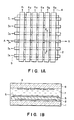
- Figure 1A is a plan view of a liquid crystal device according to the present invention used in an optical switch array
- Figure 1B is a sectional view taken along the line A-B in Figure 1A.
- the liquid crystal device shown in Figures 1A and 1B is a liquid crystal cell having a cell gap of 100 ⁇ m obtained through uniaxial alignment control treatment such as rubbing or oblique vapor deposition.
- the liquid crystal cell comprises two 1 mm-thick glass substrates 1 and 6 provided with ITO electrodes and a ferroelectric liquid crystal 7 disposed therebetween.
- a ferroelectric liquid crystal 7 (chiral smectic C liquid crystal) such as MBRA-8 (4-O-(2-methyl)-butylresorcylidene-4 ⁇ -octylaniline) showing a ferroelectric phase at room temperature under a supercooled state was used.
- an auxiliary electrode 2 of ITO was formed on the first glass substrate by vapor deposition, and the auxiliary electrode 2 was covered with a 50 ⁇ m-thick dielectric film 3 of glass (SiO2) or plastic on which signal electrodes (I1, I2, ...) 5 of ITO were formed in the form of stripes. Further, on the second glass substrates 6, scanning electrodes (S1, S2, ...) 4 also of ITO were formed in the form of stripes.
- the liquid crystal device was driven in the following manner as shown in Figure 2. More specifically, the scanning electrodes 4 were used as common electrodes, and an AC voltage was uniformly applied between the auxiliary electrode 2 and the scanning electrodes 4 by means of an AC voltage supply 9. Further, a DC voltage was applied to an arbitrary one of the signal electrodes 5 composed of stripe-form ITO films through a resistor R (10).
- the resistor R was used because an AC bias electric field is not substantially applied to the liquid crystal layer 7 due to a shielding effect if the signal electrodes 5 are of a low impedance. In order to effectively apply an AC bias electric field, it is preferred to connect a resistor R of 100 K ⁇ to 10 M ⁇ .
- the liquid crystal cell becomes turbid to assume a minimum transmittance.
- a certain DC bias is applied to an intersection of a selected scanning electrode 4 and a selected signal electrode 5, the clarity of the intersection (pixel) is increased to provide an increased transmittance. Accordingly, if the DC bias is variably controlled by means of a variable DC supply, the transmittance through the optical switch can be changed.
- the cell gap of the ferroelectric liquid crystal cell may generally be set to a range of 10 ⁇ m to 100 ⁇ m.
- Figure 4 is a graph showing voltage waveforms applied in the embodiment and the resultant change in transmittance in comparison.
- a contrast of 200:1 was obtained by superposing an AC voltage V AC with a frequency of 350 Hz and a peak voltage of 800 Vpp and a DC bias V DC of 100 V. Further, a high-speed optical response on the order of sub-milliseconds was realized.
- Figure 3 shows an arrangement of an optical system by which the transmittance through the above optical switch.
- a test beam issued from a He-Ne laser 31 as a light source is passed through an expanding-and-collimating system including lenses 32 and 33 and incident on the optical switch 34 as a test piece.
- the light beam transmitted through the optical switch 34 is focused through a condenser lens 35 and a pin-hole 36 and detected by a silicon photosensor cell.
- the transmitted light quantity when the transmitted light quantity is plotted versus the AC voltage applied to the liquid crystal cell with the transmitted light quantity under no electric field being taken as the standard (1) of a relative scale, the transmitted light quantity remains at nearly 1 at a frequency of 1400 Hz and approaches 2 at a frequency of 2800 Hz.
- the frequency for providing the liquid crystal with a turbidity is below about 1 KHz, and at a higher frequency, the voltage application rather increases the clarity.
- the saturation value changes depending on the cell thickness, so that the frequency of the AC voltage may generally be selected from the range of 200 Hz to 2 KHz.
- the AC voltage is substantially decreased because of capacitance division with the dielectric film 3, so that the magnitude thereof must be decreased by that much.
- Figure 5 shows a characteristic curve showing a relation between the transmitted light quantity and the DC voltage signal when various DC voltage signals were superposed on an AC voltage with a frequency of 350 Hz and a voltage peak value Vpp of 800 volts.
- the voltage of the DC signal is in the range of -100 V to +100 V for a cell gap of 100 ⁇ m.
- the AC voltage may be generally set in the range of 100 V to 1000 V in terms of a peak-to-peak voltage while it can vary depending on the kind of ferroelectric liquid crystal used and the cell gap.
- a scanning selection signal may be sequentially applied to the scanning electrodes 4, and in phase with the scanning selection signal, an information signal may be applied to the signal electrodes 5 so that the above-mentioned DC bias component may be applied to an intersection of a selected scanning electrode 4 and a selected signal electrode 4. Further, at this time, the above DC bias component may be set to a value corresponding to gradation data given to the respective pixels.
- an information signal comprising a peak value, a pulse duration or a number of pulses depending on given gradation data may be supplied to each pixel through a signal electrode 5.
- FIG. 8 is a block diagram of a driving apparatus used in the present invention.
- Image signals are once stored in a line memory circuit 81 and supplied through a latch circuit 82 to a D/A converter where they are subjected to digital/analog conversion to supply signal voltages V ON and V OFF selectively to signal electrodes 5.
- a ring counter 86 provided with resistors R11, R12, a capacitor C1 and a transistor Tr for each scanning electrode, whereby a voltage V1 is applied to a selected scanning electrode and a voltage V2 is applied to a nonselected scanning electrode.
- the auxiliary electrode 2 is always supplied with an AC voltage from an AC power supply 84.
- a voltage of V ON - V1 is applied to a selected pixel on a selected scanning electrode, and a voltage of V OFF - V1 is applied to a nonselected scanning electrode on the same scanning electrode.
- a voltage of V ON - V2 or V OFF - V2 is applied to pixels on a nonselected scanning electrode.
- the voltage V ON - V1 is set to a value exceeding the threshold voltage ⁇ V th shown in Figure 5, and the voltages V OFF - V1, V ON - V2 AND V OFF - V2 are set to a value not exceeding the threshold voltage ⁇ V th .
- the peak values of voltages V ON - V2 and V OFF - V2 may be set to below 1/2, preferably below 1/3, of the peak value of the voltage V ON - V1 so as to prevent the occurrence of crosstalk.
- MBRA-8 was used as a ferroelectric liquid crystal.
- ferroelectric liquid crystals as disclosed in, e.g., "LE JOURNAL DE PHYSIQUE LETTERS” 36 (L-69), 1975 “Ferroelectric Liquid Crystals”; “Applied Physics Letters” 36 (11) 1980, “Submicro- Second Bistable Electrooptic Switching in Liquid Crystals", “Kotai Butsuri (Solid State Physics)” 16 (141), 1981 “Liquid Crystal”; U.S. Patents Nos. 4561726, 4589996, 4596667, 4613209, 4614609, 4622165, 4639089, etc.
- ferroelectric liquid crystal compound usable in the present invention examples include decyloxybenzylidene-p ⁇ -amino-2-methylbutyl cinnamate (DOBAMBC), hexyloxybenzylidene-p ⁇ -amino-2-chloropropyl cinnamate (HOBACPC), 4-O-(2-methyl)butylresorcylidene-4 ⁇ -octylaniline (MBRA 8), etc.
- DOBAMBC decyloxybenzylidene-p ⁇ -amino-2-methylbutyl cinnamate
- HOBACPC hexyloxybenzylidene-p ⁇ -amino-2-chloropropyl cinnamate
- MBRA 8 4-O-(2-methyl)butylresorcylidene-4 ⁇ -octylaniline
- the device When a device is constituted by using these materials, the device may be supported with a block of copper, aluminum, etc., in which a heater is embedded in order to realize a temperature condition where the liquid crystal compounds assume an SmC*, SmH*, SmI*, SmF* or SmG* phase.
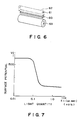
- FIG. 6 is a schematic perspective view showing an optical system wherein an optical modulation signal is supplied to a light-receiving medium 63 such as an ordinary photosensitive drum for electrophotography by using an optical switch array device according to the present invention.
- the optical system includes an elongated light source 61 such as a fluorescent lamp or an LED array and a light-reflecting hood 62. It is possible to dispose an optical means such as a Selfor lens array (not shown) between the optical switch array 60 and the light-receiving medium 63.
- the optical transmission state is controlled by modulating the transmitted light quantity basically for each pixel aperture.
- Figure 7 is a graph showing a typical example of relationship between exposed light quantity E and surface potential V for an ordinary light-receiving member or photosensitive member such as Se, amorphous-Si and OPC (organic photoconductor). So as to fit the light quantity to a gradation range as shown in Figure 7, the light source 61, the optical switch array 62 and/or the light-receiving member 63 may be driven.
- an ordinary light-receiving member or photosensitive member such as Se, amorphous-Si and OPC (organic photoconductor).
- an optical modulation device using a ferroelectric liquid crystal adapted to an optical switch array and a display panel providing a high contrast and a high response speed.
- a liquid crystal optical device has an advantage that the use of a polarizer can be omitted to obtain an increased transmittance compared with a conventional liquid crystal optical devices, so that it can provide a high contrast and a display of a wide visual field angle.
- an liquid crystal optical switch obtained according to the present invention can effect very high-speed switching on the order of sub-milliseconds, so that it can provide gradational signals at a high density to a light-receiving member for use in an electrophotographic printer, etc., to provide good printed images.
- the liquid crystal device according to the present invention is formed with a relatively large cell gap in the range of 10 ⁇ m - 200 ⁇ m, so that the cell designing therefor is easy compared with a ferroelectric liquid crystal panel proposed heretofore.
Landscapes
- Physics & Mathematics (AREA)
- Chemical & Material Sciences (AREA)
- Crystallography & Structural Chemistry (AREA)
- Engineering & Computer Science (AREA)
- General Physics & Mathematics (AREA)
- Nonlinear Science (AREA)
- Computer Hardware Design (AREA)
- Theoretical Computer Science (AREA)
- Optics & Photonics (AREA)
- Liquid Crystal (AREA)
Applications Claiming Priority (6)
| Application Number | Priority Date | Filing Date | Title |
|---|---|---|---|
| JP199034/86 | 1986-08-27 | ||
| JP61199034A JP2515509B2 (ja) | 1986-08-27 | 1986-08-27 | 光スイツチの駆動方式 |
| JP153110/87 | 1987-06-18 | ||
| JP15311087A JPS63316028A (ja) | 1987-06-18 | 1987-06-18 | 液晶装置 |
| JP20442587A JPS6446731A (en) | 1987-08-17 | 1987-08-17 | Optical modulator |
| JP204425/87 | 1987-08-17 |
Publications (3)
| Publication Number | Publication Date |
|---|---|
| EP0257638A2 true EP0257638A2 (de) | 1988-03-02 |
| EP0257638A3 EP0257638A3 (en) | 1988-12-14 |
| EP0257638B1 EP0257638B1 (de) | 1994-01-26 |
Family
ID=27320402
Family Applications (1)
| Application Number | Title | Priority Date | Filing Date |
|---|---|---|---|
| EP87112410A Expired - Lifetime EP0257638B1 (de) | 1986-08-27 | 1987-08-26 | Vorrichtung zur optischen Modulation |
Country Status (3)
| Country | Link |
|---|---|
| US (1) | US4773738A (de) |
| EP (1) | EP0257638B1 (de) |
| DE (1) | DE3788909T2 (de) |
Cited By (4)
| Publication number | Priority date | Publication date | Assignee | Title |
|---|---|---|---|---|
| EP0389211A3 (de) * | 1989-03-20 | 1991-10-02 | Fujitsu Limited | Flüssigkristall-Anzeigevorrichtung |
| EP0661583A3 (de) * | 1993-12-28 | 1996-07-24 | Shimadzu Corp | Lichtmodulator mit dicher Flüssigkristallzelle. |
| EP0782123A1 (de) * | 1995-12-27 | 1997-07-02 | Canon Kabushiki Kaisha | Flüssigkristalleinrichtung und Steuerverfahren zur Verhinderung des Vergelbungsphänomens |
| EP0865022A3 (de) * | 1988-03-24 | 1999-12-15 | Denso Corporation | Elektrooptische Einrichtung mit einem ferroelektrischen Flüssigkristall und Methode zu deren Herstellung |
Families Citing this family (36)
| Publication number | Priority date | Publication date | Assignee | Title |
|---|---|---|---|---|
| DE3815399A1 (de) * | 1987-05-08 | 1988-11-17 | Seikosha Kk | Verfahren zur ansteuerung einer optischen fluessigkristalleinrichtung |
| JPS6418194A (en) * | 1987-07-14 | 1989-01-20 | Seikosha Kk | Driving of liquid crystal display device |
| JPH0412326A (ja) * | 1990-05-01 | 1992-01-16 | Canon Inc | 液晶素子 |
| JP2835787B2 (ja) * | 1991-03-22 | 1998-12-14 | キヤノン株式会社 | 強誘電性液晶素子 |
| JP2737032B2 (ja) * | 1991-03-28 | 1998-04-08 | キヤノン株式会社 | 液晶セル |
| JP2847331B2 (ja) * | 1991-04-23 | 1999-01-20 | キヤノン株式会社 | 液晶表示装置 |
| JP2952075B2 (ja) * | 1991-06-12 | 1999-09-20 | キヤノン株式会社 | 液晶素子の製造法 |
| US5798746A (en) * | 1993-12-27 | 1998-08-25 | Semiconductor Energy Laboratory Co., Ltd. | Liquid crystal display device |
| US6184962B1 (en) * | 1997-03-05 | 2001-02-06 | Canon Kabushiki Kaisha | Liquid crystal display device with visible peripheral non-display region having masking sub-electrodes |
| TW387997B (en) * | 1997-12-29 | 2000-04-21 | Hyundai Electronics Ind | Liquid crystal display and fabrication method |
| TW484117B (en) | 1999-11-08 | 2002-04-21 | Semiconductor Energy Lab | Electronic device |
| TW522374B (en) * | 2000-08-08 | 2003-03-01 | Semiconductor Energy Lab | Electro-optical device and driving method of the same |
| US6992652B2 (en) | 2000-08-08 | 2006-01-31 | Semiconductor Energy Laboratory Co., Ltd. | Liquid crystal display device and driving method thereof |
| US6987496B2 (en) * | 2000-08-18 | 2006-01-17 | Semiconductor Energy Laboratory Co., Ltd. | Electronic device and method of driving the same |
| US7180496B2 (en) | 2000-08-18 | 2007-02-20 | Semiconductor Energy Laboratory Co., Ltd. | Liquid crystal display device and method of driving the same |
| TW518552B (en) | 2000-08-18 | 2003-01-21 | Semiconductor Energy Lab | Liquid crystal display device, method of driving the same, and method of driving a portable information device having the liquid crystal display device |
| TW514854B (en) * | 2000-08-23 | 2002-12-21 | Semiconductor Energy Lab | Portable information apparatus and method of driving the same |
| JP4014831B2 (ja) * | 2000-09-04 | 2007-11-28 | 株式会社半導体エネルギー研究所 | El表示装置及びその駆動方法 |
| KR100823047B1 (ko) | 2000-10-02 | 2008-04-18 | 가부시키가이샤 한도오따이 에네루기 켄큐쇼 | 자기발광 장치 및 그 구동 방법 |
| US7184014B2 (en) * | 2000-10-05 | 2007-02-27 | Semiconductor Energy Laboratory Co., Ltd. | Liquid crystal display device |
| US6747623B2 (en) * | 2001-02-09 | 2004-06-08 | Semiconductor Energy Laboratory Co., Ltd. | Liquid crystal display device and method of driving the same |
| JP2003114646A (ja) * | 2001-08-03 | 2003-04-18 | Semiconductor Energy Lab Co Ltd | 表示装置及びその駆動方法。 |
| TWI273539B (en) * | 2001-11-29 | 2007-02-11 | Semiconductor Energy Lab | Display device and display system using the same |
| JP3913534B2 (ja) * | 2001-11-30 | 2007-05-09 | 株式会社半導体エネルギー研究所 | 表示装置及びこれを用いた表示システム |
| JP4067878B2 (ja) * | 2002-06-06 | 2008-03-26 | 株式会社半導体エネルギー研究所 | 発光装置及びそれを用いた電気器具 |
| US6982727B2 (en) * | 2002-07-23 | 2006-01-03 | Broadcom Corporation | System and method for providing graphics using graphical engine |
| US7502040B2 (en) * | 2004-12-06 | 2009-03-10 | Semiconductor Energy Laboratory Co., Ltd. | Display device, driving method thereof and electronic appliance |
| US20060139265A1 (en) * | 2004-12-28 | 2006-06-29 | Semiconductor Energy Laboratory Co., Ltd. | Driving method of display device |
| US20060158399A1 (en) | 2005-01-14 | 2006-07-20 | Semiconductor Energy Laboratory Co., Ltd. | Driving method of display device |
| US8633919B2 (en) * | 2005-04-14 | 2014-01-21 | Semiconductor Energy Laboratory Co., Ltd. | Display device, driving method of the display device, and electronic device |
| US7719526B2 (en) | 2005-04-14 | 2010-05-18 | Semiconductor Energy Laboratory Co., Ltd. | Display device, and driving method and electronic apparatus of the display device |
| EP1720148A3 (de) * | 2005-05-02 | 2007-09-05 | Semiconductor Energy Laboratory Co., Ltd. | Anzeigevorrichtung und Verfahren mit Unterrahmen zur Ansteuerung von Graustufen |
| KR101404582B1 (ko) * | 2006-01-20 | 2014-06-09 | 가부시키가이샤 한도오따이 에네루기 켄큐쇼 | 표시장치의 구동방법 |
| US9443455B2 (en) | 2011-02-25 | 2016-09-13 | Semiconductor Energy Laboratory Co., Ltd. | Display device having a plurality of pixels |
| JP2012234080A (ja) * | 2011-05-06 | 2012-11-29 | Japan Display East Co Ltd | 表示装置 |
| WO2013172220A1 (en) | 2012-05-18 | 2013-11-21 | Semiconductor Energy Laboratory Co., Ltd. | Pixel circuit, display device, and electronic device |
Family Cites Families (9)
| Publication number | Priority date | Publication date | Assignee | Title |
|---|---|---|---|---|
| CH529421A (de) * | 1971-03-30 | 1972-10-15 | Bbc Brown Boveri & Cie | Schaltungsanordnung zur Aussteuerung matrixförmig adressierbarer flüssigkristalliner Lichtventile |
| GB1557199A (en) * | 1976-01-06 | 1979-12-05 | Standard Telephones Cables Ltd | Liquid crystal display cells |
| US4563059A (en) * | 1983-01-10 | 1986-01-07 | Clark Noel A | Surface stabilized ferroelectric liquid crystal devices |
| US4367924A (en) * | 1980-01-08 | 1983-01-11 | Clark Noel A | Chiral smectic C or H liquid crystal electro-optical device |
| GB2067811B (en) * | 1980-01-16 | 1983-08-10 | Standard Telephones Cables Ltd | Co-ordinate addressing of smetic display cells |
| FR2523343A1 (fr) * | 1982-03-09 | 1983-09-16 | Thomson Csf | Ecran d'un dispositif de visualisation utilisant un effet mixte thermique et electrique |
| AU584867B2 (en) * | 1983-12-09 | 1989-06-08 | Seiko Instruments & Electronics Ltd. | A liquid crystal display device |
| FR2557719B1 (fr) * | 1984-01-03 | 1986-04-11 | Thomson Csf | Dispositif de visualisation a memoire utilisant un materiau ferroelectrique |
| US4617646A (en) * | 1984-06-29 | 1986-10-14 | International Business Machines Corporation | Electric field gradient excited liquid crystal cell having bistability |
-
1987
- 1987-08-25 US US07/090,241 patent/US4773738A/en not_active Expired - Lifetime
- 1987-08-26 DE DE3788909T patent/DE3788909T2/de not_active Expired - Fee Related
- 1987-08-26 EP EP87112410A patent/EP0257638B1/de not_active Expired - Lifetime
Cited By (6)
| Publication number | Priority date | Publication date | Assignee | Title |
|---|---|---|---|---|
| EP0865022A3 (de) * | 1988-03-24 | 1999-12-15 | Denso Corporation | Elektrooptische Einrichtung mit einem ferroelektrischen Flüssigkristall und Methode zu deren Herstellung |
| EP0389211A3 (de) * | 1989-03-20 | 1991-10-02 | Fujitsu Limited | Flüssigkristall-Anzeigevorrichtung |
| US5113273A (en) * | 1989-03-20 | 1992-05-12 | Fujitsu Limited | Liquid crystal display device |
| EP0661583A3 (de) * | 1993-12-28 | 1996-07-24 | Shimadzu Corp | Lichtmodulator mit dicher Flüssigkristallzelle. |
| US5670978A (en) * | 1993-12-28 | 1997-09-23 | Shimadzu Corporation | Light modulator using an asymetrically-driven ferroelectric liquid crystal thick cell |
| EP0782123A1 (de) * | 1995-12-27 | 1997-07-02 | Canon Kabushiki Kaisha | Flüssigkristalleinrichtung und Steuerverfahren zur Verhinderung des Vergelbungsphänomens |
Also Published As
| Publication number | Publication date |
|---|---|
| DE3788909D1 (de) | 1994-03-10 |
| EP0257638B1 (de) | 1994-01-26 |
| US4773738A (en) | 1988-09-27 |
| EP0257638A3 (en) | 1988-12-14 |
| DE3788909T2 (de) | 1994-05-26 |
Similar Documents
| Publication | Publication Date | Title |
|---|---|---|
| EP0257638B1 (de) | Vorrichtung zur optischen Modulation | |
| EP0228557B1 (de) | Optische Modulationsvorrichtung und ihre Steuerungsmethode | |
| US5633652A (en) | Method for driving optical modulation device | |
| KR100505924B1 (ko) | 액정표시장치 및 그 구동방법 | |
| JP2549433B2 (ja) | 電気光学変調素子の駆動方法およびプリンタ | |
| US5177475A (en) | Control of liquid crystal devices | |
| EP0510606B1 (de) | Flüssigkristallanzeigevorrichtung | |
| US4932759A (en) | Driving method for optical modulation device | |
| GB2136185A (en) | Time-sharing driving method | |
| US5822031A (en) | Liquid crystal device | |
| GB2153129A (en) | Liquid crystal display devices | |
| US5293534A (en) | Liquid crystal device | |
| US4709994A (en) | Liquid crystal device using ferroelectric liquid crystal twisted in two stable states | |
| EP0298460A2 (de) | Bildererzeugungsgerät | |
| EP0469531B1 (de) | Flüssigkristallgerät und Verfahren zum Steuern dieses Gerätes | |
| US6339416B1 (en) | Antiferroelectric liquid crystal display and method of driving | |
| US5093737A (en) | Method for driving a ferroelectric optical modulation device therefor to apply an erasing voltage in the first step | |
| KR100710015B1 (ko) | 자발 분극을 갖는 액정 재료를 함유하는 표시 패널 | |
| US4802744A (en) | Optical modulation apparatus | |
| JP2584235B2 (ja) | 画像形成装置及びその駆動方法 | |
| EP0424944B1 (de) | Ferroelektrische Flüssigkristallvorrichtung | |
| JPH0415454B2 (de) | ||
| GB2217089A (en) | Display device | |
| EP0344753A2 (de) | Flüssigkristallgerät und Verfahren zum Steuern dieses Gerätes | |
| JPS62257131A (ja) | 液晶素子の駆動方法 |
Legal Events
| Date | Code | Title | Description |
|---|---|---|---|
| PUAI | Public reference made under article 153(3) epc to a published international application that has entered the european phase |
Free format text: ORIGINAL CODE: 0009012 |
|
| 17P | Request for examination filed |
Effective date: 19870827 |
|
| AK | Designated contracting states |
Kind code of ref document: A2 Designated state(s): DE FR GB IT NL |
|
| PUAL | Search report despatched |
Free format text: ORIGINAL CODE: 0009013 |
|
| AK | Designated contracting states |
Kind code of ref document: A3 Designated state(s): DE FR GB IT NL |
|
| 17Q | First examination report despatched |
Effective date: 19910711 |
|
| GRAA | (expected) grant |
Free format text: ORIGINAL CODE: 0009210 |
|
| AK | Designated contracting states |
Kind code of ref document: B1 Designated state(s): DE FR GB IT NL |
|
| REF | Corresponds to: |
Ref document number: 3788909 Country of ref document: DE Date of ref document: 19940310 |
|
| ITF | It: translation for a ep patent filed | ||
| ET | Fr: translation filed | ||
| PLBE | No opposition filed within time limit |
Free format text: ORIGINAL CODE: 0009261 |
|
| STAA | Information on the status of an ep patent application or granted ep patent |
Free format text: STATUS: NO OPPOSITION FILED WITHIN TIME LIMIT |
|
| 26N | No opposition filed | ||
| REG | Reference to a national code |
Ref country code: GB Ref legal event code: IF02 |
|
| PGFP | Annual fee paid to national office [announced via postgrant information from national office to epo] |
Ref country code: FR Payment date: 20030808 Year of fee payment: 17 |
|
| PGFP | Annual fee paid to national office [announced via postgrant information from national office to epo] |
Ref country code: GB Payment date: 20030820 Year of fee payment: 17 |
|
| PGFP | Annual fee paid to national office [announced via postgrant information from national office to epo] |
Ref country code: NL Payment date: 20030831 Year of fee payment: 17 |
|
| PGFP | Annual fee paid to national office [announced via postgrant information from national office to epo] |
Ref country code: DE Payment date: 20030904 Year of fee payment: 17 |
|
| PG25 | Lapsed in a contracting state [announced via postgrant information from national office to epo] |
Ref country code: GB Free format text: LAPSE BECAUSE OF NON-PAYMENT OF DUE FEES Effective date: 20040826 |
|
| PG25 | Lapsed in a contracting state [announced via postgrant information from national office to epo] |
Ref country code: NL Free format text: LAPSE BECAUSE OF NON-PAYMENT OF DUE FEES Effective date: 20050301 Ref country code: DE Free format text: LAPSE BECAUSE OF NON-PAYMENT OF DUE FEES Effective date: 20050301 |
|
| GBPC | Gb: european patent ceased through non-payment of renewal fee |
Effective date: 20040826 |
|
| PG25 | Lapsed in a contracting state [announced via postgrant information from national office to epo] |
Ref country code: FR Free format text: LAPSE BECAUSE OF NON-PAYMENT OF DUE FEES Effective date: 20050429 |
|
| NLV4 | Nl: lapsed or anulled due to non-payment of the annual fee |
Effective date: 20050301 |
|
| REG | Reference to a national code |
Ref country code: FR Ref legal event code: ST |
|
| PG25 | Lapsed in a contracting state [announced via postgrant information from national office to epo] |
Ref country code: IT Free format text: LAPSE BECAUSE OF NON-PAYMENT OF DUE FEES;WARNING: LAPSES OF ITALIAN PATENTS WITH EFFECTIVE DATE BEFORE 2007 MAY HAVE OCCURRED AT ANY TIME BEFORE 2007. THE CORRECT EFFECTIVE DATE MAY BE DIFFERENT FROM THE ONE RECORDED. Effective date: 20050826 |