EP0469531B1 - Flüssigkristallgerät und Verfahren zum Steuern dieses Gerätes - Google Patents
Flüssigkristallgerät und Verfahren zum Steuern dieses Gerätes Download PDFInfo
- Publication number
- EP0469531B1 EP0469531B1 EP91112750A EP91112750A EP0469531B1 EP 0469531 B1 EP0469531 B1 EP 0469531B1 EP 91112750 A EP91112750 A EP 91112750A EP 91112750 A EP91112750 A EP 91112750A EP 0469531 B1 EP0469531 B1 EP 0469531B1
- Authority
- EP
- European Patent Office
- Prior art keywords
- pixel
- orientation state
- voltage
- liquid crystal
- applying
- Prior art date
- Legal status (The legal status is an assumption and is not a legal conclusion. Google has not performed a legal analysis and makes no representation as to the accuracy of the status listed.)
- Expired - Lifetime
Links
- 239000004973 liquid crystal related substance Substances 0.000 title claims abstract description 42
- 238000000034 method Methods 0.000 title claims description 17
- 239000005262 ferroelectric liquid crystals (FLCs) Substances 0.000 claims description 19
- 210000004027 cell Anatomy 0.000 description 16
- 210000002858 crystal cell Anatomy 0.000 description 5
- 239000000758 substrate Substances 0.000 description 5
- 239000004990 Smectic liquid crystal Substances 0.000 description 4
- 238000010586 diagram Methods 0.000 description 4
- 230000000694 effects Effects 0.000 description 3
- 239000011521 glass Substances 0.000 description 3
- 230000010287 polarization Effects 0.000 description 3
- 230000002269 spontaneous effect Effects 0.000 description 3
- 230000007704 transition Effects 0.000 description 3
- VYPSYNLAJGMNEJ-UHFFFAOYSA-N Silicium dioxide Chemical compound O=[Si]=O VYPSYNLAJGMNEJ-UHFFFAOYSA-N 0.000 description 2
- 230000002411 adverse Effects 0.000 description 2
- 230000005684 electric field Effects 0.000 description 2
- 238000007789 sealing Methods 0.000 description 2
- 102100029397 Chloride channel CLIC-like protein 1 Human genes 0.000 description 1
- 101710168340 Chloride channel CLIC-like protein 1 Proteins 0.000 description 1
- 239000004642 Polyimide Substances 0.000 description 1
- 241000519995 Stachys sylvatica Species 0.000 description 1
- 230000003098 cholesteric effect Effects 0.000 description 1
- 239000011248 coating agent Substances 0.000 description 1
- 238000000576 coating method Methods 0.000 description 1
- 229910052681 coesite Inorganic materials 0.000 description 1
- 150000001875 compounds Chemical class 0.000 description 1
- 230000008878 coupling Effects 0.000 description 1
- 238000010168 coupling process Methods 0.000 description 1
- 238000005859 coupling reaction Methods 0.000 description 1
- 229910052906 cristobalite Inorganic materials 0.000 description 1
- 239000013078 crystal Substances 0.000 description 1
- 239000004744 fabric Substances 0.000 description 1
- 239000007788 liquid Substances 0.000 description 1
- 239000011159 matrix material Substances 0.000 description 1
- 239000000203 mixture Substances 0.000 description 1
- 229920001778 nylon Polymers 0.000 description 1
- 229920001721 polyimide Polymers 0.000 description 1
- 239000002243 precursor Substances 0.000 description 1
- 239000000377 silicon dioxide Substances 0.000 description 1
- 238000004544 sputter deposition Methods 0.000 description 1
- 229910052682 stishovite Inorganic materials 0.000 description 1
- 229910052905 tridymite Inorganic materials 0.000 description 1
Images

Classifications
-
- G—PHYSICS
- G09—EDUCATION; CRYPTOGRAPHY; DISPLAY; ADVERTISING; SEALS
- G09G—ARRANGEMENTS OR CIRCUITS FOR CONTROL OF INDICATING DEVICES USING STATIC MEANS TO PRESENT VARIABLE INFORMATION
- G09G3/00—Control arrangements or circuits, of interest only in connection with visual indicators other than cathode-ray tubes
- G09G3/20—Control arrangements or circuits, of interest only in connection with visual indicators other than cathode-ray tubes for presentation of an assembly of a number of characters, e.g. a page, by composing the assembly by combination of individual elements arranged in a matrix no fixed position being assigned to or needed to be assigned to the individual characters or partial characters
- G09G3/34—Control arrangements or circuits, of interest only in connection with visual indicators other than cathode-ray tubes for presentation of an assembly of a number of characters, e.g. a page, by composing the assembly by combination of individual elements arranged in a matrix no fixed position being assigned to or needed to be assigned to the individual characters or partial characters by control of light from an independent source
- G09G3/36—Control arrangements or circuits, of interest only in connection with visual indicators other than cathode-ray tubes for presentation of an assembly of a number of characters, e.g. a page, by composing the assembly by combination of individual elements arranged in a matrix no fixed position being assigned to or needed to be assigned to the individual characters or partial characters by control of light from an independent source using liquid crystals
- G09G3/3611—Control of matrices with row and column drivers
- G09G3/3622—Control of matrices with row and column drivers using a passive matrix
- G09G3/3629—Control of matrices with row and column drivers using a passive matrix using liquid crystals having memory effects, e.g. ferroelectric liquid crystals
- G09G3/3637—Control of matrices with row and column drivers using a passive matrix using liquid crystals having memory effects, e.g. ferroelectric liquid crystals with intermediate tones displayed by domain size control
-
- G—PHYSICS
- G09—EDUCATION; CRYPTOGRAPHY; DISPLAY; ADVERTISING; SEALS
- G09G—ARRANGEMENTS OR CIRCUITS FOR CONTROL OF INDICATING DEVICES USING STATIC MEANS TO PRESENT VARIABLE INFORMATION
- G09G2310/00—Command of the display device
- G09G2310/06—Details of flat display driving waveforms
-
- G—PHYSICS
- G09—EDUCATION; CRYPTOGRAPHY; DISPLAY; ADVERTISING; SEALS
- G09G—ARRANGEMENTS OR CIRCUITS FOR CONTROL OF INDICATING DEVICES USING STATIC MEANS TO PRESENT VARIABLE INFORMATION
- G09G2310/00—Command of the display device
- G09G2310/06—Details of flat display driving waveforms
- G09G2310/061—Details of flat display driving waveforms for resetting or blanking
-
- G—PHYSICS
- G09—EDUCATION; CRYPTOGRAPHY; DISPLAY; ADVERTISING; SEALS
- G09G—ARRANGEMENTS OR CIRCUITS FOR CONTROL OF INDICATING DEVICES USING STATIC MEANS TO PRESENT VARIABLE INFORMATION
- G09G2310/00—Command of the display device
- G09G2310/06—Details of flat display driving waveforms
- G09G2310/065—Waveforms comprising zero voltage phase or pause
-
- G—PHYSICS
- G09—EDUCATION; CRYPTOGRAPHY; DISPLAY; ADVERTISING; SEALS
- G09G—ARRANGEMENTS OR CIRCUITS FOR CONTROL OF INDICATING DEVICES USING STATIC MEANS TO PRESENT VARIABLE INFORMATION
- G09G3/00—Control arrangements or circuits, of interest only in connection with visual indicators other than cathode-ray tubes
- G09G3/20—Control arrangements or circuits, of interest only in connection with visual indicators other than cathode-ray tubes for presentation of an assembly of a number of characters, e.g. a page, by composing the assembly by combination of individual elements arranged in a matrix no fixed position being assigned to or needed to be assigned to the individual characters or partial characters
- G09G3/2007—Display of intermediate tones
- G09G3/2011—Display of intermediate tones by amplitude modulation
-
- G—PHYSICS
- G09—EDUCATION; CRYPTOGRAPHY; DISPLAY; ADVERTISING; SEALS
- G09G—ARRANGEMENTS OR CIRCUITS FOR CONTROL OF INDICATING DEVICES USING STATIC MEANS TO PRESENT VARIABLE INFORMATION
- G09G3/00—Control arrangements or circuits, of interest only in connection with visual indicators other than cathode-ray tubes
- G09G3/20—Control arrangements or circuits, of interest only in connection with visual indicators other than cathode-ray tubes for presentation of an assembly of a number of characters, e.g. a page, by composing the assembly by combination of individual elements arranged in a matrix no fixed position being assigned to or needed to be assigned to the individual characters or partial characters
- G09G3/2007—Display of intermediate tones
- G09G3/207—Display of intermediate tones by domain size control
Definitions
- the present invention relates to a liquid crystal apparatus particularly a ferroelectric liquid crystal apparatus, and a liquid crystal driving method.
- Display devices using a ferroelectric liquid crystal have been known, including a type wherein a ferroelectric liquid crystal (hereinafter sometimes abbreviated as "FLC") is injected into a cell or panel formed by disposing a pair of glass plates each having an inner surface provided with a transparent electrode and an aligning treatment opposite to each other so that their inner surfaces face each other with a cell gap of about 1 - 3 microns therebetween (as disclosed in, e.g., Japanese Laid-Open Patent Application (JP-A) 61-94023).
- FLC ferroelectric liquid crystal
- the above type of display device using a ferroelectric liquid crystal is characterized in that a ferroelectric liquid crystal has a spontaneous polarization causing a coupling with an external electric field available for switching and in that the switching can be caused depending on the polarity of the external electric field because the director ((longer) molecular axis direction) of each FLC molecule corresponds to the direction of its spontaneous polarization in a one-to-one correspondence.
- a ferroelectric liquid crystal is generally utilized in its chiral smectic (SmC*, SmH*, etc.) phase so that the liquid crystal molecular axes are disposed to show a twisted alignment in its bulk state but the twisting of the liquid crystal molecular axes can be released or suppressed by disposing the ferroelectric liquid crystal in a cell having a cell gap on the order of 01 - 3 microns as described above (N.A. Clark, et al., MCLC (1983), Vol. 94, p.p. 213 - 234).
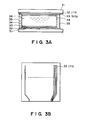
- a simple matrix-structure e.g., as shown in Figures 3A and 3B may be adopted.
- such an FLC cell or panel has a sectional structure as shown in Figure 3B and includes a pair of upper and lower glass substrates 31 each having ITO stripe electrodes 32, an SiO 2 insulating film 33 and a polyimide alignment film 34 disposed in this order thereon, a ferroelectric liquid crystal 36 disposed between the substrates, and a sealing member 35 sealing the periphery of the cell structure.
- the ITO stripe electrodes 32 are disposed on one substrate 31, e.g., in a pattern as shown in Figure 3B, so as to intersect with the stripe electrodes 32 on the other substrate 32.
- V thW denotes a threshold for writing "white” in a “white” pixel after once clearing the pixel into "black”
- V thB denotes a threshold for writing "white” in a “black” pixel after once clearing the pixel into “black”
- a relationship of V thB > V thW exhibits until a certain relaxation time lapses since the clearing into "black”.
- the resultant display state can be different depending on whether the pixel in question has been in "white” state or "black” state before the writing. This is quite awkward for a display device.
- the US-A-4 932 759 discloses a liquid crystal driving apparatus and a method for driving the same, including a liquid crystal device comprising a plurality of scanning electrodes, a plurality of data electrodes intersecting said scanning electrodes, and a bistable liquid crystal showing a first stable orientation state and a second stable orientation state disposed between said scanning electrodes and said data electrodes so as to form a pixel at each intersection of said scanning electrodes and said data electrodes.
- the described apparatus and method of driving the same includes at least two repeating sets of phases each set of phases comprising a state-determining phase for determining the contrast of a pixel and an auxiliary phase for not determining the contrast of a pixel.
- document EP-A-0 214 857 describes a similar liquid crystal driving apparatus and a method for driving the same which uses a time sharing driving for obtaining grey levels and which additionally resets the respective pixels so as to bring them into a predetermined state.
- a gradation display as well as a high-speed motion picture display
- a high-speed motion picture display which is free from flickering in case of refresh drive.
- this desired gradational state is securely reached.
- the standing time from clearing to writing of a pixel can be optimally reduced and an intended gradation state can be displayed without depending on different initial states before writing by consecutively applying two voltage application steps.
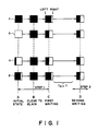
- Figure 1 is a schematic view for illustrating an embodiment of the liquid crystal driving method according to the present invention.
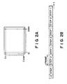
- Figures 2A and 2B are schematic views for illustrating another embodiment of the liquid crystal driving method according to the present invention.
- Figure 3A is a schematic sectional view of a conventional ferroelectric liquid crystal device
- Figure 3B is a schematic plan view showing an example of an electrode pattern thereof.
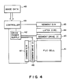
- Figure 4 is a block diagram of a drive circuit for generating drive signals for performing the liquid crystal driving method according to the present invention.
- Figure 5 is a waveform diagram showing an example of a driving waveform applied to a pixel for performing the liquid crystal driving method according to the present invention.
- Figure 6 is a graph showing a change with time of difference in switching threshold of a ferroelectric liquid crystal depending on a difference in state before writing.
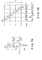
- Figures 7A and 7B are waveform diagrams showing an example set of driving waveforms for the liquid crystal driving method according to the present invention.
- voltage signals applied to the respective pixels of the liquid crystal device are divided and consecutively applied in steps 1 and 2, respectively, so that a desired state is reliably displayed in each pixel regardless of the state of the pixel before the writing.
- a desired gradation level is stably written in the respective pixels without being affected by the previous state of each pixel.
- a gradational state close to the desired level can be accomplished by performing the step 1 without having a wait time corresponding to the relaxation time in which the writing threshold affected by the previous states become substantially the same. Accordingly, it is possible to provide the display with a continuity, which is suitably applicable to a motion picture display and which is free from flickering in case of refresh drive.
- a plurality of scanning electrodes and a plurality of data electrodes are disposed to intersect each other so as to receive the respective signals, and a liquid crystal showing a first orientation state and a second orientation state is disposed between the two types of electrodes so as to form a pixel at each intersection of the scanning electrodes and the data electrodes.
- the liquid crystal at each pixel is driven between the first and second orientation states.
- the pixel is first supplied with a voltage sufficient to cause the second orientation state and then supplied with a voltage of at least V 1 which is a threshold voltage for converting a pixel in the second orientation state into the first orientation state after applying a clearing voltage for causing the second orientation state to the pixel in the first orientation state (Step 1), and then supplied with a voltage of at least V 2 which is a threshold voltage for converting a pixel in the second orientation state into the first orientation state after applying a clearing voltage for causing the second orientation state to the pixel in the second orientation state (Second step).
- a pixel in the first orientation state is securely brought to the first orientation state and, in the second step, a pixel in the second orientation state is securely brought to the first orientation state even when the pixel is not brought to the first orientation state in the first step.
- the pixel in order to provide a desired gradation level K at a certain pixel, the pixel is first supplied with a voltage sufficient to cause the second orientation state completely and then supplied with a voltage Va which is a voltage capable of providing the gradation level K to a pixel completely in the second orientation state after applying a clearing voltage for causing the second orientation state to the pixel in the first orientation state (Step 1), and then supplied with a voltage Vb which is a voltage capable of providing the gradation level K to a pixel completely in the second orientation state after applying a clearing voltage for causing the second orientation to thee pixel in the second orientation state (Step 2).
- the pixel is brought to the gradation level K in the first orientation state.
- the certain pixel is between the gradation level K and the complete second orientation state, the pixel is securely brought to the gradation level K in the second step even if the gradation level K is not provided in the first orientation state and remains to be between the gradation level K and the complete second orientation state.
- Va and Vb are ordinarily almost the same or closer to each other, a pixel at the gradation level K already in the first step does not change the gradation level.
- a desired gradation level can be stably written in a pixel without being affected by a previous display state of the pixel.
- the step 1 may be performed to obtain a gradation level close to the desired gradation level without having a wait time within which Va and Vb become substantially the same value. Accordingly, the display is caused to acquire a continuity, thus being suitable for a motion picture display and free from flickering in the case of refresh drive.
- the first and second steps may be performed in this order one by one in successive two scanning times.
- the liquid crystal suitably used in the present invention may comprise a ferroelectric liquid crystal.
- a ferroelectric liquid crystal a liquid crystal compound or composition showing chiral smectic phase as disclosed in U.S. Patent Nos. 4561726, 4614609, 4589996, 4592858, 4596667, 4613209, etc., may be used.
- a ferroelectric liquid crystal device was prepared in the following manner.
- An electrode plate was provided by coating a polished glass substrate with an ITO film having a sheet resistivity of about 40 ohm.-square by sputtering.
- Each electrode plate was further coated with a polyimde precursor liquid ("LQ-1802", mfd. by Hitachi Kasei K.K.), followed by curing and rubbing in one direction with a nylon fiber (about 0.3 mm-long)-planted cloth to form a polyimide-type alignment film.
- a pair of the class plates thus provided were fixed to each other so that their rubbing directions are identical to form a blank cell with a cell gap of about 1.4 micron.
- the blank cell was then filled with a liquid crystal A having a Ps (spontaneous polarization) of 6.6 nC/cm 2 , a ⁇ (dielectric anisotropy) of -0.3 and a tilt angle of 14.3 degrees, respectively at 30 °C, and showing the following phase transition series:
- FIG. 4 is a block diagram of an embodiment of the liquid crystal apparatus according to the present invention including a liquid crystal cell or panel 41 thus prepared and a drive circuit therefor, which includes a drive power supply 42 for generating voltages supplied to the liquid crystal cell 41, segment-side drive IC 43 for applying voltages from the drive power supply 42 to data signal lines of the liquid crystal cell 41 as image data signals, a latch circuit 44, a segment-side S/R (shift register) 45, a common-side drive IC for applying a voltage from the drive power supply 42 to scanning signal lines of the liquid crystal cell 41 as a scanning signal, a common side S/R (shift register) 47, an image data source 48, and a controller 49 for controlling the segment-side S/R 45 and the common-side S/R 47 based on image data from the image data source 48.
- a drive power supply 42 for generating voltages supplied to the liquid crystal cell 41
- segment-side drive IC 43 for applying voltages from the drive power supply 42 to data signal lines of the liquid crystal cell 41 as image
- Figure 5 shows an example of a voltage signal (pixel signal) waveform conventionally applied to pixel of the liquid crystal cell 41 according the above arrangement.
- a voltage signal (pixel signal) waveform conventionally applied to pixel of the liquid crystal cell 41 according the above arrangement.
- Figure 5 shows a waveform for clearing a pixel into “black” and then writing the pixel into “white”, including a clearing pulse P1 into "black” and a writing pulse P2 for "white”.
- the switching threshold V th may cause changes as shown in Figure 6 depending on the length of the period T.
- the curve 61 connecting black spots ( ⁇ ) represents a change in threshold V thB for clearing a pixel in "black” state before writing into “black” and then writing "white”
- the curve 62 connecting white spots (o) represents a change in threshold V thW for clearing a pixel in "white” state before writing into "black” and then writing "white”.
- a relationship of V thB - V thW > 1.0 holds for a relatively short period T. The difference in threshold cannot be ignored for writing by application of voltages in the neighborhood of the threshold and leads to a difficulty in display of gradation levels.
- a period T of about 44 msec is required in order that the difference between V thB and V thW can be ignored. During the period, flickering is caused even in a refresh drive, giving rise to a difficulty in a display device. Further, in the case of a gradational display, the difference can result in display gradation level amounting to about 5 - 10 %.
- FIG. 1 is a schematic view for illustrating a transition of states of four pixels a - d having different initial states. From the left to right in Figure 1, at A are shown initial states, at B are shown states after clearing into "black”, at C are shown states after a first writing, and at D are shown states after a second writing for the pixels a - d, respectively.
- the pixels a - d are respectively assumed to have a square region having a threshold gradually increasing from the left side toward the right side. Such a threshold change within a pixel may be caused according to a cell gap change within the range of 1.0 - 1.4 micron for a pixel.
- This embodiment is constituted by two steps including a first step of from clearing into "black” up to application of a gradation data signal for the first time, and a second step of applying a gradation data signal for the second time.
- a first-time gradation data signal is assumed to be an inversion signal for causing an inversion of, e.g., 50 % of pixel.
- a writing (rewriting) in a second step is performed after a lapse of time T 0 which is larger than a relaxation time T of approximately 44 msec (beyond which a difference in threshold disappears).
- the pixels a - d are initially at the states C .
- the writing signal may have a switching threshold Vop (15.0 volts) from the "black" state.
- the pixels having the initial states a and d are completely written with 50 %-inversion data.
- the pixels having the initials b and c which have been already written with complete gradation data also have the same switching threshold from the "black" state with respect to their black-written regions.
- all the pixels a - d are written at the same intended gradation level.
- an intended gradation state can be displayed without depending on different initial states before writing by consecutively applying two voltage application steps of the step 1 and the step 2. Further, even at a stage after the step 1, the gradation data are written to some extent, so that the display can be provided with a continuity and may be applicable to a motion picture display compared with the case where a whole picture or screen is allowed to stand at the initial state of "white” or "black” for the above-mentioned relaxation time T.
- the standing time can be reduced to an order of microseconds or substantially omitted according to this embodiment.
- the steps 1 and 2 are divided into two consecutive frames each comprises scanning of all the scanning lines, an intended graditional picture can be displayed with an error of about 10 % in a step 1, followed by a step 2 providing a completely intended gradational picture free of error.
- the above frame scanning time is assumed to be 100 msec for example, the influence of the previous pixel states can be completely removed if the above-mentioned relaxation time is 100 msec or shorter.
- pixels b and c having a lower threshold voltage for the desired gradation level are written in Step 1, but it is also possible to write pixels a and d having a higher threshold voltage for the desired gradation level in Step 1 if an additional step of clearing into "black" is placed before Step 2.
- This embodiment is directed to an application of the present invention to a binary state display.
- a display device comprising 400 scanning lines C 1 - C 400 and 640 data signal lines S 1 - S 640 as shown in Figure 2A is driven by applying driving voltages which are changed for each frame scanning (of 400 lines) so that steps 1 and 2 as described in the previous embodiment are performed are alternating frames as shown in Figure 2.
- the liquid crystal device structure is the same as in the first embodiment except that the cell gap is uniformly 1.4 micron.
- This embodiment is effective for ensuring a reliable writing over a wide liquid crystal device (a panel rather than a cell) having a certain difference in operation temperature, which also results in a difference in switching threshold voltages so that an entire panel cannot be written by a single writing signal voltage.
- an A4 size panel resulted in a temperature difference of 2 °C ranging from 34 °C to 36 °C due to a local difference in heat generated by the drive IC.
Landscapes
- Engineering & Computer Science (AREA)
- Chemical & Material Sciences (AREA)
- Crystallography & Structural Chemistry (AREA)
- Physics & Mathematics (AREA)
- Computer Hardware Design (AREA)
- General Physics & Mathematics (AREA)
- Theoretical Computer Science (AREA)
- Liquid Crystal (AREA)
- Liquid Crystal Display Device Control (AREA)
- Liquid Crystal Substances (AREA)
Claims (4)
- Flüssigkristall-Ansteuerungsverfahren mit den Schritten
Ausbilden einer Flüssigkristalleinrichtung mit einer Vielzahl von Abtastelektroden (C1 - C400), einer Vielzahl von die Abtastelektroden (C1 - C400) überkreuzenden Datenelektroden (S1 - S640) und einem bistabilen Flüssigkristall (36), der einen ersten stabilen Orientierungszustand und einen zweiten stabilen Orientierungszustand zeigt und zwischen den Abtastelektroden (C1 - C400) und den Datenelektroden (S1 - S640) angeordnet ist, um an jeder Überkreuzung der Abtastelektroden und der Datenelektroden ein Bildelement auszubilden,
gekennzeichnet durch
die Schreibschritte zum Bewirken des ersten Orientierungszustands bei einem Bildelement miteinem ersten Schritt zum Anlegen einer vorgeschriebenen Spannung (Ve) an das Bildelement zum Bewirken des zweiten Orientierungszustands und daraufhin zum Anlegen einer ersten Spannung V1st an das Bildelement undeinem zweiten Schritt zum Anlegen einer zweiten Spannung V2nd an das Bildelement,wobei die erste Spannung V1st und die zweite Spannung V2nd jeweils zumindest V1 und zumindest V2 oder jeweils Va und Vb sind,wobei V1 eine Schwellenspannung (VthW) bezeichnet, die zur Umwandlung eines Bildelements in dem zweiten Orientierungszustand in den ersten Orientierungszustand nach dem Anlegen der vorgeschriebenen Spannung (Ve) an das Bildelement in dem ersten Orientierungszustand zum Bewirken des zweiten Orientierungszustands erforderlich ist, und V2 eine Schwellenspannung (VthB) bezeichnet, die zur Umwandlung eines Bildelements in dem zweiten Orientierungszustand in den ersten Orientierungszustand nach dem Anlegen der vorgeschriebenen Spannung (Ve) an das Bildelement in dem zweiten Orientierungszustand zum Bewirken des zweiten Orientierungszustands erforderlich ist,wobei Va eine Spannung bezeichnet, die zur Umwandlung eines sich vollständig in dem zweiten Orientierungszustand befindenden Bildelements in den Abstufungspegel k nach dem Anlegen der vorgeschriebenen Spannung (Ve) an das sich vollständig in dem ersten Orientierungszustand befindende Bildelement zum Bewirken des zweiten Orientierungszustands erforderlich ist, und Vb eine Spannung bezeichnet, die zur Umwandlung eines sich vollständig in dem zweiten Orientierungszustand befindenden Bildelements in den Abstufungspegel k nach dem Anlegen der vorgeschriebenen Spannung (Ve) an das sich vollständig in dem zweiten Orientierungszustand befindende Bildelement zum Bewirken des zweiten Orientierungszustands erforderlich ist, undwobei der erste Schritt zu einem Zeitpunkt durchgeführt wird, wenn jeweils V1 < V2 oder Va < Vb ist, und der zweite Schritt zu einem Zeitpunkt durchgeführt wird, wenn jeweils V1 und V2 oder Va und Va im wesentlichen identisch zueinander sind. - Flüssigkristall-Ansteuerungsvorrichtung mit
einer Flüssigkristalleinrichtung mit einer Vielzahl von Abtastelektroden (C1 - C400), einer Vielzahl von die Abtastelektroden (C1 - C400) überkreuzenden Datenelektroden (S1 - S640) und einem bistabilen Flüssigkristall (36), der einen ersten stabilen Orientierungszustand und einen zweiten stabilen Orientierungszustand zeigt und zwischen den Abtastelektroden (C1 - C400) und den Datenelektroden (S1 - S640) angeordnet ist, um an jeder Überkreuzung der Abtastelektroden und der Datenelektroden ein Bildelement auszubilden,
gekennzeichnet durcheine Ansteuerungseinrichtung (42 - 49) zum Bewirken des ersten Orientierungszustands bei einem Bildelement in zwei Schritten miteinem ersten Schritt zum Anlegen einer vorgeschriebenen Spannung (Ve) an das Bildelement zum Bewirken des zweiten Orientierungszustands und daraufhin zum Anlegen einer ersten Spannung V1st an das Bildelement, undeinem zweiten Schritt zum Anlegen einer zweiten Spannung V2nd an das Bildelement,wobei die erste Spannung V1st und die zweite Spannung V2nd jeweils zumindest V1 und zumindest V2, oder jeweils Va und Vb sind,wobei V1 eine Schwellenspannung (VthW) bezeichnet, die zur Umwandlung eines Bildelements in dem zweiten Orientierungszustand in den ersten Orientierungszustand nach dem Anlegen der vorgeschriebenen Spannung (Ve) an das Bildelement in dem ersten Orientierungszustand zum Bewirken des zweiten Orientierungszustands erforderlich ist, und V2 eine Schwellenspannung (VthB) bezeichnet, die zur Umwandlung eines Bildelements in dem zweiten Orientierungszustand in den ersten Orientierungszustand nach dem Anlegen der vorgeschriebenen Spannung (Ve) an das Bildelement in dem zweiten Orientierungszustand zum Bewirken des zweiten Orientierungszustands erforderlich ist,wobei Va eine Spannung bezeichnet, die zur Umwandlung eines sich vollständig in dem zweiten Orientierungszustand befindenden Bildelements in den Abstufungspegel k nach dem Anlegen der vorgeschriebenen Spannung (Ve) an das sich vollständig in dem ersten Orientierungszustand befindende Bildelement zum Bewirken des zweiten Orientierungszustands erforderlich ist, und Vb eine Spannung bezeichnet, die zur Umwandlung eines sich vollständig in dem zweiten Orientierungszustand befindenden Bildelements in den Abstufungspegel k nach dem Anlegen der vorgeschriebenen Spannung (Ve) an das sich vollständig in dem zweiten Orientierungszustand befindende Bildelement zum Bewirken des zweiten Orientierungszustands erforderlich ist, undwobei der erste Schritt zu einem Zeitpunkt durchgeführt wird, wenn jeweils V1 < V2 oder Va < Vb ist, und der zweite Schritt zu einem Zeitpunkt durchgeführt wird, wenn jeweils V1 und V2 oder Va und Vb im wesentlichen identisch zueinander sind. - Verfahren oder Vorrichtung nach Anspruch 1 oder 2, dadurch gekennzeichnet, daß
der erste Schritt und der zweite Schritt jeweils in dieser Reihenfolge bei aufeinanderfolgenden zwei Abtastzeiten für das Bildelement durchgeführt werden. - Verfahren oder Vorrichtung nach Anspruch 1 oder 2, dadurch gekennzeichnet, daß
der Flüssigkristall (36) ein ferroelektrischer Flüssigkristall ist.
Applications Claiming Priority (2)
| Application Number | Priority Date | Filing Date | Title |
|---|---|---|---|
| JP199133/90 | 1990-07-30 | ||
| JP2199133A JP2915104B2 (ja) | 1990-07-30 | 1990-07-30 | 液晶素子および液晶駆動方法 |
Publications (3)
| Publication Number | Publication Date |
|---|---|
| EP0469531A2 EP0469531A2 (de) | 1992-02-05 |
| EP0469531A3 EP0469531A3 (en) | 1993-01-27 |
| EP0469531B1 true EP0469531B1 (de) | 1997-04-02 |
Family
ID=16402695
Family Applications (1)
| Application Number | Title | Priority Date | Filing Date |
|---|---|---|---|
| EP91112750A Expired - Lifetime EP0469531B1 (de) | 1990-07-30 | 1991-07-29 | Flüssigkristallgerät und Verfahren zum Steuern dieses Gerätes |
Country Status (5)
| Country | Link |
|---|---|
| US (1) | US5379138A (de) |
| EP (1) | EP0469531B1 (de) |
| JP (1) | JP2915104B2 (de) |
| AT (1) | ATE151190T1 (de) |
| DE (1) | DE69125427T2 (de) |
Families Citing this family (14)
| Publication number | Priority date | Publication date | Assignee | Title |
|---|---|---|---|---|
| JP2802685B2 (ja) * | 1991-01-08 | 1998-09-24 | キヤノン株式会社 | 強誘電性液晶装置 |
| JP2847331B2 (ja) * | 1991-04-23 | 1999-01-20 | キヤノン株式会社 | 液晶表示装置 |
| DE69219828T2 (de) * | 1991-07-24 | 1997-10-16 | Canon Kk | Datenanzeige |
| DE69317640T2 (de) * | 1992-12-28 | 1998-07-30 | Canon Kk | Verfahren und Einrichtung für eine Flüssigkristallanzeige |
| US5592190A (en) * | 1993-04-28 | 1997-01-07 | Canon Kabushiki Kaisha | Liquid crystal display apparatus and drive method |
| US6219019B1 (en) * | 1996-09-05 | 2001-04-17 | Kabushiki Kaisha Toshiba | Liquid crystal display apparatus and method for driving the same |
| US6452581B1 (en) | 1997-04-11 | 2002-09-17 | Canon Kabushiki Kaisha | Driving method for liquid crystal device and liquid crystal apparatus |
| US6177968B1 (en) | 1997-09-01 | 2001-01-23 | Canon Kabushiki Kaisha | Optical modulation device with pixels each having series connected electrode structure |
| JP3347678B2 (ja) | 1998-06-18 | 2002-11-20 | キヤノン株式会社 | 液晶素子とその駆動方法 |
| KR100695923B1 (ko) * | 1998-10-22 | 2007-03-20 | 시티즌 워치 콤파니, 리미티드 | 강유전성 액정 표시 소자 및 이의 구동 방법 |
| KR100890092B1 (ko) * | 2001-05-08 | 2009-03-24 | 타이코 일렉트로닉스 레이켐 케이. 케이. | 회로 보호 장치 |
| JP5047461B2 (ja) * | 2002-05-29 | 2012-10-10 | ゼットビーディー ディスプレイズ リミテッド | ディスプレイデバイス |
| JP2008544313A (ja) * | 2005-06-17 | 2008-12-04 | コーニンクレッカ フィリップス エレクトロニクス エヌ ヴィ | 双安定ディスプレイ装置の駆動システム及び方法 |
| US8933869B2 (en) | 2008-03-27 | 2015-01-13 | Citizen Holdings Co., Ltd. | Ferroelectric liquid crystal panel driving method and liquid crystal display device |
Family Cites Families (19)
| Publication number | Priority date | Publication date | Assignee | Title |
|---|---|---|---|---|
| US4613209A (en) * | 1982-03-23 | 1986-09-23 | At&T Bell Laboratories | Smectic liquid crystals |
| EP0115693B1 (de) * | 1983-01-06 | 1987-08-26 | Chisso Corporation | Flüssigkristallverbindungen und Mischungen derselben |
| US4614609A (en) * | 1983-06-14 | 1986-09-30 | Chisso Corporation | Liquid crystalline biphenyl derivatives and mixtures thereof |
| US4561726A (en) * | 1983-07-29 | 1985-12-31 | At&T Bell Laboratories | Alignment of ferroelectric LCDs |
| JPS6054341A (ja) * | 1983-09-05 | 1985-03-28 | Chisso Corp | 液晶性炭酸エステル類 |
| JPS60218358A (ja) * | 1984-04-13 | 1985-11-01 | Ajinomoto Co Inc | 液晶 |
| JPS6152630A (ja) * | 1984-08-22 | 1986-03-15 | Hitachi Ltd | 液晶素子の駆動方法 |
| JPS6167833A (ja) * | 1984-09-11 | 1986-04-08 | Citizen Watch Co Ltd | 液晶表示装置 |
| JPS6186732A (ja) * | 1984-10-04 | 1986-05-02 | Canon Inc | 液晶装置 |
| JPS6194023A (ja) * | 1984-10-15 | 1986-05-12 | Canon Inc | 液晶素子 |
| JPS61156229A (ja) * | 1984-12-28 | 1986-07-15 | Canon Inc | 液晶装置 |
| US4707078A (en) * | 1985-04-26 | 1987-11-17 | American Telephone And Telegraph Company, At&T Bell Laboratories | Ferroelectric liquid crystal devices using field-stabilized states |
| DE3686462T2 (de) * | 1985-09-06 | 1993-01-21 | Matsushita Electric Ind Co Ltd | Verfahren zur ansteuerung eines fluessigkristallrasterbildschirmes. |
| JPS62119521A (ja) * | 1985-11-19 | 1987-05-30 | Canon Inc | 光学変調装置 |
| JPS62150334A (ja) * | 1985-12-25 | 1987-07-04 | Canon Inc | 液晶装置 |
| US4770502A (en) * | 1986-01-10 | 1988-09-13 | Hitachi, Ltd. | Ferroelectric liquid crystal matrix driving apparatus and method |
| GB2173629B (en) * | 1986-04-01 | 1989-11-15 | Stc Plc | Addressing liquid crystal cells |
| GB8720856D0 (en) * | 1987-09-04 | 1987-10-14 | Emi Plc Thorn | Matrix addressing |
| US5151803A (en) * | 1989-01-09 | 1992-09-29 | Matsushita Electric Industrial Co., Ltd. | Pixel-gap controlled ferroelectric liquid crystal display device and its driving method |
-
1990
- 1990-07-30 JP JP2199133A patent/JP2915104B2/ja not_active Expired - Fee Related
-
1991
- 1991-07-29 DE DE69125427T patent/DE69125427T2/de not_active Expired - Fee Related
- 1991-07-29 AT AT91112750T patent/ATE151190T1/de not_active IP Right Cessation
- 1991-07-29 EP EP91112750A patent/EP0469531B1/de not_active Expired - Lifetime
-
1994
- 1994-02-15 US US08/196,800 patent/US5379138A/en not_active Expired - Fee Related
Also Published As
| Publication number | Publication date |
|---|---|
| DE69125427D1 (de) | 1997-05-07 |
| JPH0485517A (ja) | 1992-03-18 |
| JP2915104B2 (ja) | 1999-07-05 |
| US5379138A (en) | 1995-01-03 |
| EP0469531A3 (en) | 1993-01-27 |
| ATE151190T1 (de) | 1997-04-15 |
| EP0469531A2 (de) | 1992-02-05 |
| DE69125427T2 (de) | 1997-10-30 |
Similar Documents
| Publication | Publication Date | Title |
|---|---|---|
| US5488388A (en) | Liquid crystal apparatus | |
| US5092665A (en) | Driving method for ferroelectric liquid crystal optical modulation device using an auxiliary signal to prevent inversion | |
| EP0229647B1 (de) | Verfahren zum Ansteuern einer Flüssigkristallanzeigematrix | |
| KR940004139B1 (ko) | 액정표시장치 및 그 구동방법 | |
| US5631752A (en) | Antiferroelectric liquid crystal display element exhibiting a precursor tilt phenomenon | |
| EP0564263B1 (de) | Anzeigegerät | |
| US5296953A (en) | Driving method for ferro-electric liquid crystal optical modulation device | |
| JPH05158444A (ja) | 液晶表示装置 | |
| US4925277A (en) | Method and apparatus for driving optical modulation device | |
| US5408246A (en) | Electro-optical modulating apparatus and driving method thereof | |
| US4932759A (en) | Driving method for optical modulation device | |
| US5379138A (en) | Bi-stable liquid crystal device and driving method which allows for time variable threshold voltages | |
| EP0605865B1 (de) | Verfahren und Einrichtung für eine Flüssigkristallanzeige | |
| JPH06258614A (ja) | 表示素子 | |
| US5724059A (en) | Method for driving optical modulation device | |
| US5973657A (en) | Liquid crystal display apparatus | |
| US20010011986A1 (en) | Method of driving antiferroelectric liquid crystal display | |
| JP3093511B2 (ja) | 表示装置 | |
| JP3101790B2 (ja) | 液晶表示素子 | |
| JPS63259516A (ja) | マトリクス型液晶表示体駆動方法 | |
| US5757350A (en) | Driving method for optical modulation device | |
| CA1258327A (en) | Driving method for optical modulation device | |
| JP3233925B2 (ja) | 強誘電液晶素子の駆動方法 | |
| JPH05323284A (ja) | 強誘電液晶表示装置 | |
| JPH06235904A (ja) | 強誘電性液晶表示素子 |
Legal Events
| Date | Code | Title | Description |
|---|---|---|---|
| PUAI | Public reference made under article 153(3) epc to a published international application that has entered the european phase |
Free format text: ORIGINAL CODE: 0009012 |
|
| 17P | Request for examination filed |
Effective date: 19910829 |
|
| AK | Designated contracting states |
Kind code of ref document: A2 Designated state(s): AT BE CH DE DK ES FR GB GR IT LI LU NL SE |
|
| PUAL | Search report despatched |
Free format text: ORIGINAL CODE: 0009013 |
|
| AK | Designated contracting states |
Kind code of ref document: A3 Designated state(s): AT BE CH DE DK ES FR GB GR IT LI LU NL SE |
|
| 17Q | First examination report despatched |
Effective date: 19940913 |
|
| GRAG | Despatch of communication of intention to grant |
Free format text: ORIGINAL CODE: EPIDOS AGRA |
|
| GRAH | Despatch of communication of intention to grant a patent |
Free format text: ORIGINAL CODE: EPIDOS IGRA |
|
| GRAH | Despatch of communication of intention to grant a patent |
Free format text: ORIGINAL CODE: EPIDOS IGRA |
|
| GRAA | (expected) grant |
Free format text: ORIGINAL CODE: 0009210 |
|
| AK | Designated contracting states |
Kind code of ref document: B1 Designated state(s): AT BE CH DE DK ES FR GB GR IT LI LU NL SE |
|
| PG25 | Lapsed in a contracting state [announced via postgrant information from national office to epo] |
Ref country code: IT Free format text: LAPSE BECAUSE OF FAILURE TO SUBMIT A TRANSLATION OF THE DESCRIPTION OR TO PAY THE FEE WITHIN THE PRESCRIBED TIME-LIMIT;WARNING: LAPSES OF ITALIAN PATENTS WITH EFFECTIVE DATE BEFORE 2007 MAY HAVE OCCURRED AT ANY TIME BEFORE 2007. THE CORRECT EFFECTIVE DATE MAY BE DIFFERENT FROM THE ONE RECORDED. Effective date: 19970402 Ref country code: CH Effective date: 19970402 Ref country code: LI Effective date: 19970402 Ref country code: NL Effective date: 19970402 Ref country code: DK Effective date: 19970402 Ref country code: GR Free format text: LAPSE BECAUSE OF FAILURE TO SUBMIT A TRANSLATION OF THE DESCRIPTION OR TO PAY THE FEE WITHIN THE PRESCRIBED TIME-LIMIT Effective date: 19970402 Ref country code: ES Free format text: THE PATENT HAS BEEN ANNULLED BY A DECISION OF A NATIONAL AUTHORITY Effective date: 19970402 Ref country code: BE Effective date: 19970402 Ref country code: AT Effective date: 19970402 |
|
| REF | Corresponds to: |
Ref document number: 151190 Country of ref document: AT Date of ref document: 19970415 Kind code of ref document: T |
|
| REG | Reference to a national code |
Ref country code: CH Ref legal event code: EP |
|
| REF | Corresponds to: |
Ref document number: 69125427 Country of ref document: DE Date of ref document: 19970507 |
|
| ET | Fr: translation filed | ||
| PG25 | Lapsed in a contracting state [announced via postgrant information from national office to epo] |
Ref country code: SE Effective date: 19970702 |
|
| PG25 | Lapsed in a contracting state [announced via postgrant information from national office to epo] |
Ref country code: LU Free format text: LAPSE BECAUSE OF NON-PAYMENT OF DUE FEES Effective date: 19970729 |
|
| NLV1 | Nl: lapsed or annulled due to failure to fulfill the requirements of art. 29p and 29m of the patents act | ||
| REG | Reference to a national code |
Ref country code: CH Ref legal event code: PL |
|
| PLBE | No opposition filed within time limit |
Free format text: ORIGINAL CODE: 0009261 |
|
| STAA | Information on the status of an ep patent application or granted ep patent |
Free format text: STATUS: NO OPPOSITION FILED WITHIN TIME LIMIT |
|
| 26N | No opposition filed | ||
| REG | Reference to a national code |
Ref country code: GB Ref legal event code: IF02 |
|
| PGFP | Annual fee paid to national office [announced via postgrant information from national office to epo] |
Ref country code: FR Payment date: 20030711 Year of fee payment: 13 |
|
| PGFP | Annual fee paid to national office [announced via postgrant information from national office to epo] |
Ref country code: GB Payment date: 20030723 Year of fee payment: 13 |
|
| PGFP | Annual fee paid to national office [announced via postgrant information from national office to epo] |
Ref country code: DE Payment date: 20030807 Year of fee payment: 13 |
|
| PG25 | Lapsed in a contracting state [announced via postgrant information from national office to epo] |
Ref country code: GB Free format text: LAPSE BECAUSE OF NON-PAYMENT OF DUE FEES Effective date: 20040729 |
|
| PG25 | Lapsed in a contracting state [announced via postgrant information from national office to epo] |
Ref country code: DE Free format text: LAPSE BECAUSE OF NON-PAYMENT OF DUE FEES Effective date: 20050201 |
|
| GBPC | Gb: european patent ceased through non-payment of renewal fee |
Effective date: 20040729 |
|
| PG25 | Lapsed in a contracting state [announced via postgrant information from national office to epo] |
Ref country code: FR Free format text: LAPSE BECAUSE OF NON-PAYMENT OF DUE FEES Effective date: 20050331 |
|
| REG | Reference to a national code |
Ref country code: FR Ref legal event code: ST |