EP0257776A2 - Circuit intégré d'application spécifique pour la coopération avec un équipement microprocesseur - Google Patents
Circuit intégré d'application spécifique pour la coopération avec un équipement microprocesseur Download PDFInfo
- Publication number
- EP0257776A2 EP0257776A2 EP87306376A EP87306376A EP0257776A2 EP 0257776 A2 EP0257776 A2 EP 0257776A2 EP 87306376 A EP87306376 A EP 87306376A EP 87306376 A EP87306376 A EP 87306376A EP 0257776 A2 EP0257776 A2 EP 0257776A2
- Authority
- EP
- European Patent Office
- Prior art keywords
- data
- register
- station
- terminal
- received
- Prior art date
- Legal status (The legal status is an assumption and is not a legal conclusion. Google has not performed a legal analysis and makes no representation as to the accuracy of the status listed.)
- Withdrawn
Links
Images


Classifications
-
- G—PHYSICS
- G06—COMPUTING OR CALCULATING; COUNTING
- G06F—ELECTRIC DIGITAL DATA PROCESSING
- G06F13/00—Interconnection of, or transfer of information or other signals between, memories, input/output devices or central processing units
-
- G—PHYSICS
- G06—COMPUTING OR CALCULATING; COUNTING
- G06F—ELECTRIC DIGITAL DATA PROCESSING
- G06F1/00—Details not covered by groups G06F3/00 - G06F13/00 and G06F21/00
- G06F1/04—Generating or distributing clock signals or signals derived directly therefrom
-
- G—PHYSICS
- G05—CONTROLLING; REGULATING
- G05B—CONTROL OR REGULATING SYSTEMS IN GENERAL; FUNCTIONAL ELEMENTS OF SUCH SYSTEMS; MONITORING OR TESTING ARRANGEMENTS FOR SUCH SYSTEMS OR ELEMENTS
- G05B19/00—Program-control systems
- G05B19/02—Program-control systems electric
- G05B19/04—Program control other than numerical control, i.e. in sequence controllers or logic controllers
- G05B19/042—Program control other than numerical control, i.e. in sequence controllers or logic controllers using digital processors
- G05B19/0423—Input/output
-
- G—PHYSICS
- G06—COMPUTING OR CALCULATING; COUNTING
- G06F—ELECTRIC DIGITAL DATA PROCESSING
- G06F13/00—Interconnection of, or transfer of information or other signals between, memories, input/output devices or central processing units
- G06F13/38—Information transfer, e.g. on bus
-
- G—PHYSICS
- G06—COMPUTING OR CALCULATING; COUNTING
- G06F—ELECTRIC DIGITAL DATA PROCESSING
- G06F3/00—Input arrangements for transferring data to be processed into a form capable of being handled by the computer; Output arrangements for transferring data from processing unit to output unit, e.g. interface arrangements
- G06F3/05—Digital input using the sampling of an analogue quantity at regular intervals of time, input from a/d converter or output to d/a converter
-
- G—PHYSICS
- G05—CONTROLLING; REGULATING
- G05B—CONTROL OR REGULATING SYSTEMS IN GENERAL; FUNCTIONAL ELEMENTS OF SUCH SYSTEMS; MONITORING OR TESTING ARRANGEMENTS FOR SUCH SYSTEMS OR ELEMENTS
- G05B2219/00—Program-control systems
- G05B2219/20—Pc systems
- G05B2219/25—Pc structure of the system
- G05B2219/25133—Serial parallel conversion
-
- G—PHYSICS
- G05—CONTROLLING; REGULATING
- G05B—CONTROL OR REGULATING SYSTEMS IN GENERAL; FUNCTIONAL ELEMENTS OF SUCH SYSTEMS; MONITORING OR TESTING ARRANGEMENTS FOR SUCH SYSTEMS OR ELEMENTS
- G05B2219/00—Program-control systems
- G05B2219/20—Pc systems
- G05B2219/25—Pc structure of the system
- G05B2219/25178—Serial communication, data, also repeater
-
- G—PHYSICS
- G05—CONTROLLING; REGULATING
- G05B—CONTROL OR REGULATING SYSTEMS IN GENERAL; FUNCTIONAL ELEMENTS OF SUCH SYSTEMS; MONITORING OR TESTING ARRANGEMENTS FOR SUCH SYSTEMS OR ELEMENTS
- G05B2219/00—Program-control systems
- G05B2219/20—Pc systems
- G05B2219/25—Pc structure of the system
- G05B2219/25258—ASIC
-
- G—PHYSICS
- G05—CONTROLLING; REGULATING
- G05B—CONTROL OR REGULATING SYSTEMS IN GENERAL; FUNCTIONAL ELEMENTS OF SUCH SYSTEMS; MONITORING OR TESTING ARRANGEMENTS FOR SUCH SYSTEMS OR ELEMENTS
- G05B2219/00—Program-control systems
- G05B2219/30—Nc systems
- G05B2219/34—Director, elements to supervisory
- G05B2219/34008—Asic application specific integrated circuit, single chip microcontroller
Definitions
- This invention relates to Application Specific Integrated Circuit devices (ASIC's) with particular reference to such devices for providing control input to and monitoring function of electrical or electromechanical apparatus with special application to domestic appliances.
- ASIC Application Specific Integrated Circuit devices
- the present inventor has developed a universal circuit for an ASIC for acting in cooperation with a typical general microprocessor control, such as the Motorola MC6805P2, which is susceptible of various pin out arrangements dependent upon the specific functionality required in any particular case.
- Criteria found to be desirable and in the ASIC herein described should provide at least the following capabilities: - 26 Segment LCD Drive (Non-Multiplexed) - LCD Backplane Drive (60 Hz) - Piezo Acoustic Annunciator drive - LCD Backlight Control - Single line Asynchronous Communication Link - 20 Key, Keyboard Matrix Input
- the device should also usefully include: - 6 Channel A/D Converter - Approximate 60 Hz "Tick" Output - Watchdog Reset for the microprocessor - MODE pin to convert some bits of LCD sigment drivers for High Current Outputs
- a circuit for cooperation with serial data sending and receiving means which comprises, a terminal for data path connection therewith, a register for serially receiving data from, and for serially feeding data to the terminal, and a storage or latch means for data in the register.
- serial data sending and receiving means such as a microprocessor
- a timing oscillator generates a shift clock signal to step the register synchronously with the serially received data from the terminal, and for serially stepping the register at a predetermined rate when serially feeding data stored in it to the terminal.
- a validating means detects presence of start and stop bit data in predetermined locations in the register thereby defining presence of a data phrase received at the terminal. Additional means detects command bit data in the phrase, and further means responsive to simultaneous output of the validating means, and the command bit data detector switches the data storage means and the register in accordance with the command bit data.
- command bit data switch is the means for feeding local data into the register.
- Output means can also be provided for driving output devices from the storage or latch means.
- a shift register can be conditioned to a plurality of states by a mode control means.
- Data can thus be received by the register either from a terminal to which the data has been fed or from a local data generating means.
- the register can also transmit data placed in it to the terminal.
- Means is responsive to data received by the shift register for actuating the mode control means.
- Both preferred versions of the ASIC are constructed in CMOS technology and adhere to the general CMOS characteristics.
- the backlight control output BCKLGT for driving the liquid crystal display for the associated appliance can source 10 mA and maintain a 2 volt minimum.
- the acoustic beeper output BEEP for an audible transducer on the appliance provides a source of 7.0V and can sink 30 mA while maintaining 1.2V min.
- BITS 0-7 and 12 of the LCD segment drivers have 14 mA minimum and 25 mA maximum source capability.
- the outputs BITS 8 to 11 and 13 to 25 are standard CMOS buffered output.
- the two versions of the ASIC share the same "core" circuitry. They are, however, designed for different applications. Version 2 does not provide signals for an LCD or interface to a keyboard. The unused I/O pins can thus be eliminated. The result is a device which fits into a conventional 28 Pin DIL package, which is a more widely used package style and can realize a significant cost improvement over the 44 pin variety for this reason alone.
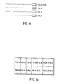
- the pin designations of the preferred form of version 2 are shown in Figure 3.
- ASIC version 2 The primary function of ASIC version 2 is to replace all of the circuitry which would otherwise have to be designed into the microprocessor and associated circuitry, i.e. that associated with the watchdog function, A/D conversion used for temperature (or other) sensing, AC signal conditioning to provide a 60 Hz interrupt and the high current drive for either direct coupling to sensitive gate triacs or the LED drive for opto-isolators used in the associated power equipment (motors, heaters, etc.).
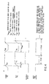
- a power-up reset or external reset to the device is activated via the /TEST input. This is an active low input and does not require any external components, although it is pinned out for test purposes.
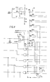
- the internal circuitry is configured in such a manner as to eliminate the need for input and comprises a hysteresis amplifier 1, and a power supply level sensor 2, feeding OR gate 3 to produce a RESET output.
- the parameters for the reset timing are shown in Figure 4. Essentially, the reset timing has been chosen to meet the requirements of the reset input of the Motorola MC6805P2 mentioned before.
- the MRST output (to be described later) of the ASIC version 2 directly drives the MC 6805P2 reset input. This function is not provided on version 1.
- the function of the /TEST input terminal is of value during the IC manufacture to speed-up test procedures.
- the actual configuration of the RESET circuit can vary as it does not affect the operation of the device in any other manner.
- the RESET signal under normal operating conditions will only occur during POWER-UP. However, momentary contact to Vss of the /TEST input will provide a device reset, proving the timing specifications apparent from Figure 4 are met.
- the circuitry shown at 5 is also involved in speeding up testing during manufacture only, during use of the ASIC the periodic appearance of the SYRST signal causes it to serve only as a connector between the penultimate and the last flip-flop in the ⁇ 9 counter chain.
- An internal Oscillator circuit 10 is provided which is stabilised by a 4MHz ceramic resonator 11 connected between XTAL and EXTAL inputs.
- the specific circuitry of the oscillator can be varied but it should preferably be capable of driving the MC6805P2 from pin EXTAL to provide a 4MHz clock for that unit.
- This type of design eliminates an additional resonator for the MC6805P2 and also ensures equivalent timing tolerances between the two devices. Overall synchronization is important during communications between the ASIC and the microprocessor.
- the output of the oscillator circuit is connected directly to the first stage 12 of the ⁇ 9 Prescaler.
- the prescaler section consists of an asynchronous ripple counter with common resets. The function of the prescaler is to reduce the 4MHz external frequency down to 7.813 KHz, which operates as the strobe (STR) signal for the system. Following the prescaler is another ⁇ 7 synchronous ripple counter which provides all of the main internal timing signals. Finally, there is an additional ⁇ 4 asynchronous ripple counter, which reduces the frequency to approximately 3.5 Hz at the MRST output. The final stage of this counter receives a RESET input to its S terminal from OR gate 3 to give a MRST output except when microprocessor reset is required. The counter can be reset on a RESET or CLKRST pulse fed to OR gate 15.
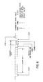
- Figure 5 illustrates the important first three mentioned above and a few additional signals which will be covered shortly.
- the ASIC is essentially a "dumb” device. It has no inherent intelligence and, therefore, requires an interface to a controlling device, such as the Motorola MC 68005P2 8-bit microprocessor.
- the ASIC is able to communicate with the controlling device via the asynchronous serial communication line connected to the bidirectional port SERIAL I/O of Figure 1.
- This port is designed to sink in the range of 10mA min, 20mA max. at 2V.
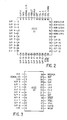
- the controller send a 32 bit message in a specific format.
- the data format adopted and as illustrated in Figure 6 does not adhere stringently to the current industry standards but has been developed specifically for use in communications with the ASIC by the assignee of this invention.
- the data string comprises a START bit, 26 INFORMATION bits, BEEPER control bit, 2 COMMAND bits and finally 2 STOP bits.
- the 26 information bits will vary depending on which command has been selected and which version of the ASIC is being used. Both ASIC versions use two command bits which gives four possible command words.
- Figure 6 also shows a truth table outlining the possible options. To facilitate better understanding of the circuit operation, the explanation will now be directed to ASIC V.1.
- the ASIC as "watchdog” switches the MRST output to the controller to a logic ONE to re-establish communications by resetting the microcomputer.
- the controlling device To maintain proper circuit operation, the controlling device must communicate properly with or "scan" the ASIC at least once every 135 mS.
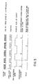
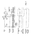
- a typical send/receive pattern between controller and ASIC is shown in Figure 7.
- the serial I/O line is at a logic "1" level. This is by virtue of the 10K internal pull-up resistor 20 and the fact that the I/O port pin of the controller is programmed as an output at a high level during initialization.
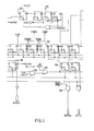
- the controller In order to initiate a data transfer, the controller must first pull the SERIAL I/O pin low (logic "0"). This negative edge propagates through the three input AND gate 21 and is inverted at 22, thus providing a positive transition to the clock input of the Shift Register Reset Control flip-flop 23. The triggering of this D Type flip-flop releases the resets of the 32 bit shift register 30 via SHFRST on the Q output.
- the Q output of flip-flop 23 provides a trigger for the clock reset control flip-flop 24.
- the Q output of this D Type flip-flop provides the signal CLKRST through OR gate 15 to the entire clock timing counter chain except the final stage. This results in reset of the counter chain.
- the broken out section of the shift clock waveform SHFCLK (the clocking waveform for register 30, obtained from the timing chain) of Figure 7 demonstrates the clock circuit reset action.
- the width of the CLKRST signal should be sufficient to guarantee a reset condition on the timing chain flip-flops. This CLKRST pulse width is obtained by feeding the output of flip-flop 24 through the three stage shift register 25 and then to the reset of flip-flop 24.
- the SHFCLK signal triggers the input stage of the 32 bit shift register 30.
- the incoming data bits from the controlling microprocessor device each have a width of approximately 256 uS. This value is fairly accurate because the MC6805P2 has an internal timer.
- the objective is to have the rising edge of the 3.907 KHz SHFCLK signal sample the incoming data at the midpoint of each data bit.
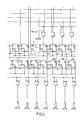
- the serial data string is thus clocked into the 32 bit shift register 30 in the previously specified data format. If the serial data string does not meet the exact specifications of the format, it will not be properly received in register 30 and thus cannot be subsequently latched into the respective output latches of latch group 31.
- VALID pulse is one-quarter of SHFCLK (approximately 64 uS). It is the rising edge of this pulse which triggers the selected function to be performed by the ASIC.
- the signal triggers the 27 bit output latch group 31 through OR gate 40 and the contents of the register 30 are transferred to the respective latches. If the command function chosen has been either LCD LATCH or BCKLGT ON/OFF there is no return information. The remaining command functions A/D LATCH and LOAD KEYBOARD STATUS would have information to be returned to the controlling device. Explanation of these two functions will be saved for another section.
- the flip-flop 17 which provides the SYSRST pulse also supplies the INT output signal which is connected directly to pin 2 (INT input) of the MC6805P2 microcomputer. This is an approximate 60 Hz interrupt to the controlling device for use as a real time clock.
- the INT signal from the ASIC occurs approximately every 16.4 mS and should always be provided, and is particularly important if the microprocessor has its one independent clock and is not driven directly by the ASIC oscillator 10, as described above. Communication between the controlling device and the ASIC should thus be synchronized to the INT signal. All send/receive information can be performed well within the 16.4 mS window.
- Figure 2 implies that the LATCH A/D function is not available on the ASIC V.1. This fact is not entirely true. As indicated earlier, both versions of the ASIC have the same circuitry. They are simply packaged differently. If all of the keyboard inputs are not used for a keyboard function, the remaining inputs may be used as analog inputs. This illustrates an aspect of the great versatility designed into the device.
- ASIC V.1 is intended primarily as an LCD driver.
- Current Liquid Crystal displays being designed into the applicant's control systems are of the transmissive type. These displays require some form of backlighting in the viewing area for the segments to be visible.
- the ASIC has an output (BCKLGT) which is capable of driving the base of a darlington transistor.
- the BCKLGT function has a command word (shown here as logic "1" for both COMM and COMM2) and is effected through AND 38 and flip-flop 45 in the same manner as already described for the LCD latch.
- An added feature is that the state of the BCKLGT control (on/off) can be read back by the controller during a keyboard scan.
- the controlling microprocessor can detect the fault during a normal keyboard scan and rectify the condition.
- the activation or deactivation of the BCKLGT control normally occurs during a change in the LCD condition. For this reason, the clock edge to the BCKLGT control flip-flop 45 also clocks the 27-output latch group 31 through OR gates 33 and 40. Two related functions may thus be accessed simultaneously.
- the BCKLGT output is not provided in the ASIC V.2.
- the BEEPER output is available through AND gate 46 from latch 48 and is essentially an approximate 2 KHz gated signal used to activate a piezo acoustic annunciator.
- the beeper control bit is bit 27 in the data string.
- the beeper activation time is approximately 200 mSec.
- the duration time is not fixed but must be a multiple of the 16.4 mSec scan rate.
- the controlling microprocessor initiates data transfer and sends the 32 bit string.
- the point of significance here is the position of the "walking ONE" within the data string.
- Bit 27 of the data string provides the walking one.
- the START, STOP and COMMAND bits must meet the proper format also. All other bits within the string are cleared to zero to ensure that a false key bit is not received by the controller.
- the ENAB signal from flip-flop 52 also goes low thus disabling the serial input circuitry at AND 21 and enabling the serial output (DATA OUT) tri-state gate amplifier 53.
- the first 10 stages of the shift register 30 still have the SHFCLK signal present.
- SHFCLK On each successive SHFCLK signal the walking ONE beginning at flip-flop 55 is shifted one position to the right. This provides successively a logic "1" at the column (Col 1-4) outputs in turn. If a key were pressed, the corresponding row input would then become high since key processing will bridge a COL and a ROW contact unique to that key.
- the combination of the COL output, ROW input and LOAD signal (from AND 56) is then unique to one member of the AND gate group 57 and will preset the corresponding flip-flop within the shift register section 49.
- the microprocessor controlling device begins to scan the serial I/O line approximately 900 uSec after it has made a keyboard scan request.
- the first bit received by the microprocessor is the START bit followed by 20 bits corresponding to the keyboard read, the state of the back light control bit (BCKBIT) and two stop bits.
- BCKBIT back light control bit
- the condition of the STOP bits sent by the ASIC is reverse to that sent by the microprocessor since the first STOP bit is now the walking ONE which has been stepped through the register and the second stop bit is the ZERO from the COMM bit in the LOAD KEYBOARD command.
- the controlling microprocessor simply requires an internal counter to determine the position of the "1" generated by the key press. Although a keyscan takes more time than the normal data send, it still does not require the full 16.4 mSec data window. After completion of the keyscan, the ASIC generates a SYSRST at flip-flop 17 through OR 16, setting itself up for the next communication sequence. Due to the length of time required by the SEND/RECEIVE sequence, it is imperative that the communication be synchronized to the 60 Hz INT output. In this way, the microprocessor timing (if using an oscillator not tied to oscillator circuit 10) is not disturbed substantially.
- keypad monitoring be done at a fairly brisk pace. At least once every 60 to 100 mSec. From this it can be seen that at least 10 to 15% of the microprocessor execution time is devoted to taking care of the keypad.
- the A/D converter works on the principle of an RC network formed by an external capacitor at the terminal (CAPIN) and an external resistor at the respective (CH1-6) input.
- the external resistance used is typically a thermistor with a negative temperature coefficient.
- the A/D circuitry uses the varying resistance to provide an analog value (voltage) for digital conversion.
- the negative input comparator 65 is connected to the RC node 66. When activated, the output of the comparator produces an output pulse after a time determined by the values of the RC network then effective at node 66, the time varying in accordance with the resistance.
- the resistive devices used typically provide 5K-50K resistance swings.
- the A/D function is principally intended for the ASIC V.2. It is however available on version 1 if at least 2 inputs are free, and all of the LCD drivers are not used.
- the normal sequence of events taking place for an A/D request is as follows.
- the channel is selected by activating one of the A-F select lines. Due to the fact that the output latches 31 are being used, it is important typically that the Bits 0-12 outputs remain unchanged since these are used for componens such as fans, motors, valves, etc. which should not be interrupted.
- the microprocessor After the microprocessor has completed the 32 bit "SEND" string including the A/D select command word, it reverses its I/O pin and begins an internal counter to determine the length of the returning pulse.
- the command word is decoded by the ASIC and disables the analog gate 67, shorting the CAPIN input to ground.
- the ENAB2 signal at flip-flop 63 activates the AND gate channel selector group 69.
- the ENAB2 signal activates the AND group 70 so that the respective ANALOG channel switches 71 can be activated. Due to the nature of the circuit, it is important that the "ON" resistance of the analog switches 71 not exceed approximately 250 ohms.
- the voltage at the negative input of the comparator 65 begins to rise by virtue of the external capacitance being charged towards VDD by the respective external resistance connected to VDD.
- the ASIC When the voltage at the negative input reaches 2/3 of VDD the output of the comparator 65 switches. The controlling microprocessor sees the falling edge and stops its internal counter to determine the equivalent digital value. After the A/D sequence is complete, the ASIC generates a SYSRST, thus resetting the device for the next sequence.
- the width of the output pulse generated by the comparator is typically 500 uS to 6 mSec.
- the A/D channels are placed within the boundaries of a byte of data.
- Figure 8 illustrates a typical A/D read.
Landscapes
- Engineering & Computer Science (AREA)
- Theoretical Computer Science (AREA)
- Physics & Mathematics (AREA)
- General Physics & Mathematics (AREA)
- General Engineering & Computer Science (AREA)
- Human Computer Interaction (AREA)
- Automation & Control Theory (AREA)
- Communication Control (AREA)
- Control By Computers (AREA)
- Information Transfer Systems (AREA)
- Input From Keyboards Or The Like (AREA)
Applications Claiming Priority (2)
| Application Number | Priority Date | Filing Date | Title |
|---|---|---|---|
| CA000515108A CA1265255A (fr) | 1986-07-31 | 1986-07-31 | Circuit integre pour usage specifique |
| CA515108 | 1986-07-31 |
Publications (2)
| Publication Number | Publication Date |
|---|---|
| EP0257776A2 true EP0257776A2 (fr) | 1988-03-02 |
| EP0257776A3 EP0257776A3 (fr) | 1989-07-19 |
Family
ID=4133665
Family Applications (1)
| Application Number | Title | Priority Date | Filing Date |
|---|---|---|---|
| EP87306376A Withdrawn EP0257776A3 (fr) | 1986-07-31 | 1987-07-17 | Circuit intégré d'application spécifique pour la coopération avec un équipement microprocesseur |
Country Status (5)
| Country | Link |
|---|---|
| US (1) | US4816823A (fr) |
| EP (1) | EP0257776A3 (fr) |
| JP (1) | JPS6399655A (fr) |
| KR (1) | KR880002082A (fr) |
| CA (1) | CA1265255A (fr) |
Cited By (2)
| Publication number | Priority date | Publication date | Assignee | Title |
|---|---|---|---|---|
| EP0568420A1 (fr) * | 1992-04-30 | 1993-11-03 | STMicroelectronics S.A. | Interface programmable notamment pour la commande d'installations domestiques |
| US5764948A (en) * | 1993-04-29 | 1998-06-09 | Sgs-Thomson Microelectronics S.A. | Method and apparatus for determining a composition of an integrated circuit |
Families Citing this family (16)
| Publication number | Priority date | Publication date | Assignee | Title |
|---|---|---|---|---|
| EP0325077B1 (fr) * | 1988-01-22 | 1992-09-09 | International Business Machines Corporation | Interface de scrutation pour les adapteurs de lignes d'une commande de communication |
| DE68928543T2 (de) * | 1988-10-06 | 1998-04-23 | Gpt Ltd | Asynchrone Zeitvielfachvermittlungsanordnung und Verfahren zum Betrieb der Anordnung |
| US5113398A (en) * | 1989-06-01 | 1992-05-12 | Shackleton System Drives Corporation | Self-healing data network and network node controller |
| US5181201A (en) * | 1990-02-07 | 1993-01-19 | General Dynamics Land Systems Inc. | Interface chip device |
| US5262625A (en) * | 1991-11-15 | 1993-11-16 | Ncr Corporation | Multiple bar code decoding system and method |
| WO1993022857A1 (fr) * | 1992-05-04 | 1993-11-11 | Ford Motor Company Limited | Circuit asservi de commande de bus pour les communications de classe a dans un vehicule a moteur |
| US5475621A (en) * | 1993-12-09 | 1995-12-12 | Pitney Bowes Inc. | Dual mode timer-counter |
| US5471608A (en) * | 1993-12-09 | 1995-11-28 | Pitney Bowes Inc. | Dynamically programmable timer-counter having enable mode for timer data load and monitoring circuit to allow enable mode only upon time-out |
| US5552991A (en) * | 1993-12-09 | 1996-09-03 | Pitney Bowes Inc. | Control system for an electronic pastage meter having a programmable application specific intergrated circuit |
| US5483458A (en) * | 1993-12-09 | 1996-01-09 | Pitney Bowes Inc. | Programmable clock module for postage metering control system |
| US5793656A (en) * | 1994-06-30 | 1998-08-11 | Hughes Electronics Corporation | Application-specific integrated circuits having programming functions |
| US5696685A (en) * | 1994-07-06 | 1997-12-09 | Pitney Bowes Inc. | Control system for an electronic postage meter having a programmable print head controller |
| KR100324734B1 (ko) * | 1995-08-04 | 2002-08-24 | 엘지전자주식회사 | 비트패턴검출장치 |
| US6792212B1 (en) * | 1997-06-17 | 2004-09-14 | The Boeing Company | Spacecraft data acquisition and distribution interface |
| US20040207864A1 (en) * | 2003-04-18 | 2004-10-21 | Combs Steven Donald | Method for operating a printer and method for operating a printer controller |
| TWM305902U (en) * | 2006-07-25 | 2007-02-01 | Fortune Semiconductor Corp | IC for facilitating to realize self-calibration, and its measuring device |
Family Cites Families (6)
| Publication number | Priority date | Publication date | Assignee | Title |
|---|---|---|---|---|
| US4130883A (en) * | 1975-10-14 | 1978-12-19 | Bethlehem Steel Corporation | Data communication system having bidirectional station interfaces |
| JPS5333546A (en) * | 1976-09-10 | 1978-03-29 | Hitachi Ltd | Communication control unit |
| US4614944A (en) * | 1982-09-30 | 1986-09-30 | Teleplex Corporation | Telemetry system for distributed equipment controls and equipment monitors |
| GB8304950D0 (en) * | 1983-02-22 | 1983-03-23 | Int Computers Ltd | Data communication systems |
| NL8503476A (nl) * | 1985-12-18 | 1987-07-16 | Philips Nv | Bussysteem. |
| CA1249886A (fr) * | 1986-05-02 | 1989-02-07 | Claude J. Champagne | Methode de transmission de donnees duplex utilisant un protocole d'emission avec attente |
-
1986
- 1986-07-31 CA CA000515108A patent/CA1265255A/fr not_active Expired - Fee Related
-
1987
- 1987-07-17 EP EP87306376A patent/EP0257776A3/fr not_active Withdrawn
- 1987-07-30 US US07/079,768 patent/US4816823A/en not_active Expired - Fee Related
- 1987-07-30 JP JP62191485A patent/JPS6399655A/ja active Pending
- 1987-07-31 KR KR1019870008459A patent/KR880002082A/ko not_active Withdrawn
Cited By (4)
| Publication number | Priority date | Publication date | Assignee | Title |
|---|---|---|---|---|
| EP0568420A1 (fr) * | 1992-04-30 | 1993-11-03 | STMicroelectronics S.A. | Interface programmable notamment pour la commande d'installations domestiques |
| FR2690766A1 (fr) * | 1992-04-30 | 1993-11-05 | Sgs Thomson Microelectronics | Interface programmable notamment pour la commande d'installations domestiques. |
| US5537651A (en) * | 1992-04-30 | 1996-07-16 | Sgs-Thomson Microelectronics S.A. | Programmable interface, notably for the control of domestic installations |
| US5764948A (en) * | 1993-04-29 | 1998-06-09 | Sgs-Thomson Microelectronics S.A. | Method and apparatus for determining a composition of an integrated circuit |
Also Published As
| Publication number | Publication date |
|---|---|
| JPS6399655A (ja) | 1988-04-30 |
| EP0257776A3 (fr) | 1989-07-19 |
| CA1265255A (fr) | 1990-01-30 |
| KR880002082A (ko) | 1988-04-29 |
| US4816823A (en) | 1989-03-28 |
Similar Documents
| Publication | Publication Date | Title |
|---|---|---|
| US4816823A (en) | Application specific integrated circuit | |
| US5805063A (en) | Wireless security sensor transmitter | |
| US5495240A (en) | Master-slave data transmission system employing a flexible single-wire bus | |
| US5809013A (en) | Message packet management in a wireless security system | |
| JPH0319740B2 (fr) | ||
| US5848277A (en) | Method for providing both level-sensitive and edge-sensitive interrupt signals on a serial interface between a peripheral and host | |
| US3747074A (en) | Method of and apparatus for baud rate detection | |
| JPS62207044A (ja) | 通信制御方法および装置 | |
| US5872512A (en) | Apparatus and method for reducing errors in a battery operated sensing circuit | |
| KR860001789B1 (ko) | 페이저 수신기 | |
| US3045063A (en) | Telegraph systems | |
| US3675240A (en) | Keyboard encoding arrangement | |
| JPS5825654Y2 (ja) | 時分割遠方制御装置 | |
| SU660052A1 (ru) | Устройство дл контрол цифровых блоков | |
| JPS6110361Y2 (fr) | ||
| JPH07283844A (ja) | 波形制御回路 | |
| KR100242691B1 (ko) | 업/다운 카운터의 카운트제어회로 | |
| SU1193656A1 (ru) | Устройство дл ввода информации | |
| KR100460029B1 (ko) | 단말기의어드레스지정방법 | |
| KR900001521B1 (ko) | 키보드의 인터페이스 회로 | |
| JPS60100248A (ja) | 入出力装置 | |
| JP2961305B2 (ja) | 伝送文字数計測装置 | |
| RU1829037C (ru) | Устройство дл контрол цифровых блоков | |
| SU1756894A1 (ru) | Устройство дл контрол цифровых узлов | |
| JP2572734B2 (ja) | シリアルデータの表示回路 |
Legal Events
| Date | Code | Title | Description |
|---|---|---|---|
| PUAI | Public reference made under article 153(3) epc to a published international application that has entered the european phase |
Free format text: ORIGINAL CODE: 0009012 |
|
| AK | Designated contracting states |
Kind code of ref document: A2 Designated state(s): DE GB SE |
|
| PUAL | Search report despatched |
Free format text: ORIGINAL CODE: 0009013 |
|
| AK | Designated contracting states |
Kind code of ref document: A3 Designated state(s): DE GB SE |
|
| STAA | Information on the status of an ep patent application or granted ep patent |
Free format text: STATUS: THE APPLICATION IS DEEMED TO BE WITHDRAWN |
|
| 18D | Application deemed to be withdrawn |
Effective date: 19900122 |
|
| RIN1 | Information on inventor provided before grant (corrected) |
Inventor name: DESNOYERS, MICHAEL Inventor name: POLKINGHORNE, JOHN |