EP0257912A2 - Statische Halbleiterspeicheranordnung - Google Patents
Statische Halbleiterspeicheranordnung Download PDFInfo
- Publication number
- EP0257912A2 EP0257912A2 EP87307107A EP87307107A EP0257912A2 EP 0257912 A2 EP0257912 A2 EP 0257912A2 EP 87307107 A EP87307107 A EP 87307107A EP 87307107 A EP87307107 A EP 87307107A EP 0257912 A2 EP0257912 A2 EP 0257912A2
- Authority
- EP
- European Patent Office
- Prior art keywords
- potential
- memory device
- channel mos
- semiconductor memory
- sense amplifier
- Prior art date
- Legal status (The legal status is an assumption and is not a legal conclusion. Google has not performed a legal analysis and makes no representation as to the accuracy of the status listed.)
- Withdrawn
Links
Images


Classifications
-
- G—PHYSICS
- G11—INFORMATION STORAGE
- G11C—STATIC STORES
- G11C11/00—Digital stores characterised by the use of particular electric or magnetic storage elements; Storage elements therefor
- G11C11/21—Digital stores characterised by the use of particular electric or magnetic storage elements; Storage elements therefor using electric elements
- G11C11/34—Digital stores characterised by the use of particular electric or magnetic storage elements; Storage elements therefor using electric elements using semiconductor devices
- G11C11/40—Digital stores characterised by the use of particular electric or magnetic storage elements; Storage elements therefor using electric elements using semiconductor devices using transistors
- G11C11/41—Digital stores characterised by the use of particular electric or magnetic storage elements; Storage elements therefor using electric elements using semiconductor devices using transistors forming static cells with positive feedback, i.e. cells not needing refreshing or charge regeneration, e.g. bistable multivibrator or Schmitt trigger
- G11C11/413—Auxiliary circuits, e.g. for addressing, decoding, driving, writing, sensing, timing or power reduction
- G11C11/417—Auxiliary circuits, e.g. for addressing, decoding, driving, writing, sensing, timing or power reduction for memory cells of the field-effect type
- G11C11/419—Read-write [R-W] circuits
-
- G—PHYSICS
- G11—INFORMATION STORAGE
- G11C—STATIC STORES
- G11C7/00—Arrangements for writing information into, or reading information out from, a digital store
- G11C7/06—Sense amplifiers; Associated circuits, e.g. timing or triggering circuits
- G11C7/062—Differential amplifiers of non-latching type, e.g. comparators, long-tailed pairs
-
- G—PHYSICS
- G11—INFORMATION STORAGE
- G11C—STATIC STORES
- G11C7/00—Arrangements for writing information into, or reading information out from, a digital store
- G11C7/10—Input/output [I/O] data interface arrangements, e.g. I/O data control circuits, I/O data buffers
- G11C7/1048—Data bus control circuits, e.g. precharging, presetting, equalising
Definitions
- This invention relates to semiconductor memory devices.
- it relates to an improved static random access memory wherein data can be read at high speed from memory cells.
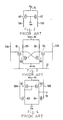
- Fig. 1 is a block diagram showing the construction of a conventional static random access memory (hereinafter abbreviated as S-RAM).
- reference numeral 10 designates static memory cells
- 11A and 11B are bit lines that receive and transmit data between these memory cells
- 12 designates word lines for simultaneously selecting cells from the aforementioned plurality of memory cells 10 in the column direction.
- Numeral 13 represents a load circuit that charges bit lines 11A and 11B at the power source potential V DD applied to power source terminal 14, 15 refers to column decoding lines that select cells from the plurality of memory cells 10 in the row direction, 16A and 16B are MOS transistors for bit line selection that transfer the data of bit lines 11A, 11B to a sense amplifier 17, 18A and 18B are input lines connected to a pair of input terminals of sense amplifier 17, and 19 is an output line of sense amplifier 17.
- Fig. 2 is a circuit diagram showing the specific construction of load circuit 13 in this conventional S-RAM.
- the source-drain paths of p-channel MOS transistors 41 and 42 are respectively inserted between each of pair of bit lines 11A and 11B and power source terminal 14 to which power source voltage V DD is applied.
- the gates of transistors 41 and 42 are connected to standard potential (V SS , or ground potential), and the two transistors 41 and 42 are thus normally conducting.
- Fig. 3 is a circuit diagram showing the specific construction of memory cells 10 in this conventional S-RAM.
- reference numerals 51 and 52 are n-channel MOS transistors serving as transfer gates
- 53 and 54 are n-channel MOS drive transistors
- 55 and 56 are high resistances serving as loads.
- One terminal of each transfer gate MOS transistor 51 and 52 is connected to one of pair of bit lines 11A and 11B, respectively, and their gates are connected in common to word line 12.
- the respective sources of drive MOS transistors 53 and 54 are connected in common to standard potential V SS .
- Their gates and drains are cross-connected, and the drains are connected to the other terminal of each MOS transistor 51 and 52 serving as transfer gates.
- each high resistance 55 and 56 is connected to the drain of one of the MOS transistors 53 and 54, respectively, while the other terminal of each resistance is connected to power source terminal 14.
- transistor 53 and high resistance 55, and transistor 54 and high resistance 56 constitute respective inverters. By connecting the inputs and outputs of these two inverters, a flip-flop circuit is formed that stores statically 1-bit data.
- Fig. 4 is a circuit diagram that shows a specific construction of sense amplifier 17 in the conventional S-RAM.
- this sense amplifier amplifies at high speed small potential differences generated on a pair of bit lines, and is constructed as shown.
- the respective sources of p-channel MOS transistors 61 and 62 are connected in common to power source terminal 14, and the gates of two transistors 61 and 62 are connected in common, the point of common connection of these gates being in turn connected to the drain of transistor 61.
- the drain of n-channel MOS transistor 63 is connected to the drain of transistor 61, and the source of this transistor 63 is connected to standard potential V SS .
- n-channel MOS transistor 64 is connected to the drain of transistor 62, and the source of this transistor 64 is connected to standard potential V SS .
- the gates of two transistors 63 and 64 are connected to input lines 18A and 18B, respectively.
- amplified data is output from the common drain of transistors 62 and 64.
- This type of sense amplifier is generally called a current mirror load type sense amplifier. Its output drive capability is high, so it is widely used.
- a memory cell 10 is selected as in the write operation, and the potential of bit lines 11A and 11B changes in accordance with the data that is read from this selected memory cell 10. These potential changes are transmitted to input lines 18A and 18B of sense amplifier 17. Sense amplifier 17 then amplifies this potential difference and outputs data corresponding to the read data of memory cell 10 from its output terminal 19. This data is output to the outside through a data output circuit, not shown.
- the power source voltage V DD usually used in an S-RAM is +5V.
- p-channel MOS transistors must be used for MOS transistors 41 and 42 employed in load circuit 13, shown in Fig. 2.
- the reason for this is that if n-channel MOS transistors are used instead of p-channel MOS transistors, the potential of the bit lines 11A and 11B is lowered from the power source voltage +3V by the amount of the threshold voltage of the n-channel MOS transistor, to which the "back-gate effect" is added.
- the potential of the bit lines 11A, 11B cannot be made more than about +1.5V. Data cannot be correctly read and written at such a potential.
- bit lines 11A and 11B since conventionally a p-channel MOS transistor is used as the load of bit lines 11A and 11B, when data read from memory cell 10 is output to bit lines 11A and 11B, their potential only falls slightly from power source voltage. The reason is that there is a limit to the size of drive MOS transistors 53 and 54 that constitute memory cell 10. They cannot be made unduly large or too much space would be required. The potential of the bit line that drops to level "L”, therefore, falls only slightly from the power source voltage. For example, if the power source voltage is +5V, the potential of one of the bit lines is +5V, while that of the other bit line will be about +4.5V. Sense amplifier 17 has to amplify this slight potential difference at high speed.
- a sense amplifier constructed as in Fig. 4 is designed to have its highest sensitivity at an input potential about midway between power source voltage V DD and standard potential V SS .
- V DD power source voltage
- V SS standard potential
- An object of this invention is to provide a static semiconductor memory device that can be operated in a stable manner even at a power source voltage lower than the normal voltage, and which can operate at high speed even with normal power source voltage.
- This invention provides a static semiconductor memory device comprising, a plurality of static memory cells for data storage, bit lines connected to the memory cells for transferring data to and from the memory cells, a sense amplifier having an input terminal, for amplifying the potential of the bit lines when data is transferred from the memory cells, and potential lowering device connected to the input terminal for lowering the potential of the input terminal of the sense amplifier to a potential corresponding to substantially the optimum sensitivity of the sense amplifier for increasing the speed of data transfer in the memory device.
- the sense amplifier can be operated at substantially its point of optimum sensitivity.
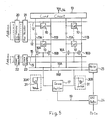
- Fig. 5 is a block diagram showing the construction of a static semiconductor memory device according to this invention.
- reference numeral 10 represents static memory cells
- 11A and 11B are bit lines that receive and transmit data between these memory cells 10
- 12 designates word lines for simultaneous selection of a plurality of these memory cells 10 in the column direction
- 13 is a load circuit that charges bit lines 11A and 11B with the power source voltage V DD applied to power source terminal 14
- 15 is a column decoding line that selects a plurality of memory cells 10 in the row direction
- 16A and 16B are MOS transistors for selecting the bit line of bit lines 11A and 11B on which the data is to be transmitted to sense amplifier
- 17A and 18B are input lines connected to a pair of input terminals of this sense amplifier 17
- 19 is the output line of sense amplifier 17
- 20 is a row address buffer
- 21 is a row decoder that selects and drives a word line 12 in accordance with the output of this row address buffer
- 22 is a column address buffer
- potential lowering circuits 30A and 30B are respectively inserted between each of the pair of input lines 18A and 18B of sense amplifier 17 and the standard potential V SS .
- N-channel MOS transistors 31 are provided in these two potential lowering circuits 30A and 30B. The sources of these transistors 31 are connected to standard potential V ss and their drains and gates are connected in common to the input lines 18A and 18B.
- Potential lowering circuits 30A and 30B are connected between respective input lines 18A and 18B of sense amplifier 17 and standard potential V SS .
- the drain and gate potentials of n-channel MOS transistors 31 exceed the sum of the threshold voltage of these transistors 31 and standard potential V SS , a current flow path is formed between respective input lines 18A and 18B and standard potential V SS .
- sense amplifier 17 is able to amplify the mutual potential difference between input lines 18A and 18B with high sensitivity, so that the stored data of memory cell 10 can be rapidly output from output terminal 19. Thus this read data is output to the outside via I/O buffer 24.
- load circuit 13 in this embodiment is constituted by a p-channel MOS transistor, in which there is no voltage drop due to threshold voltage, the potentials of bit lines 11A and 11B can be raised to power source voltage V DD . This means that stable operation can be achieved even with low power source voltage. Furthermore, because of the provision of potential lowering circuits 30A and 30B, the input potential can be set to a potential near the point of maximum sensitivity of sense amplifier 17, thereby making it possible to achieve high-speed data reading even when operating with the normal, high power source voltage.
- Figs. 6 to 8 are circuit diagrams showing the construction of potential lowering circuit 30A and 30B used in memory devices according to respective further embodiments of this invention.
- a p-channel MOS transistor 32 is used instead of n-channel MOS transistor 31.
- the gate of this transistor 32 is connected to standard potential V SS .
- a resistance 33 is used instead of n-channel MOS transistor 31.
- the potential of one or the other of input lines 18A and 18B is set to "A" level by write circuit 25, and the potential of the opposite input line is set to "L" level.
- Fig. 9 is a block diagram showing the construction of a further embodiment of this invention constructed to prevent such an increase in power consumption during data writing.
- a write enable signal is supplied to the gate of n-channel MOS transistor 31 in potential lowering circuits 30A and 30B, such that conduction of transistors 31 is controlled in accordance with this signal .
- This write enable signal is a signal that is made active ("L" level) only during data writing. The operation of write circuit 25 is controlled by means of this signal , although not shown in the Figures.
- transistor 31 is made conductive only when signal is made non-active, i.e., during data reading. Consequently, during data writing, when signal is made active, no current path is formed from input lines 18A and 18B to standard potential V SS , so unnecessary power consumption is suppressed.
- a p-channel MOS transistor can be used in place of n-channel MOS transistor 31. In this case, a signal WE would be supplied to the gate of this p-channel MOS transistor.
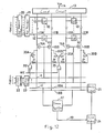
- Fig. 10 is a block diagram showing the construction of a static semiconductor memory device according to this invention.
- each bit line 11A and the standard potential V SS there is also inserted, between each bit line 11A and the standard potential V SS , the source-drain path of a p-channel MOS transistor 30A, and between each bit line 11B and the standard potential V SS , the source-drain path of a p-channel MOS transistor 30B, respectively.
- the gates of each pair of transistors 30A and 30B are connected in common to corresponding column decoding line 15.
- load circuit 13, memory cell 10, and sense amplifier 17 in this embodiment may be the same as in Fig. 2, Fig. 3 and Fig. 4, described above.
- bit lines 11A and 11B are charged up to power source potential V DD by p-channel MOS transistors 41 and 42 in load circuit 13, of which a specific configuration is shown in Fig. 2.
- the potential of bit lines 11A and 11B that are connected to this cell varies in accordance with the data that is read out from the selected memory cell.
- bit lines 11A and 11B stays at power source potential V DD , but the potential of the other bit line drops slightly from power source potential V DD , in accordance with the read data. Further, when this data is read, a specific column decoder line 15 is selected in accordance with the output of column decoder 23, causing transistors 16A and 16B to conduct.
- bit lines 11A and 11B and input lines 18A and 18B are now connected through transistors 16A and 16B, p-channel MOS transistors 30A and 30B that are connected to bit lines 11A and 11B become conductive. When these two transistors 30A and 30B become conductive, a current path is formed between respective bit lines 11A and 11B and standard ground potential V SS .
- bit lines 11A and 11B that are selected by column decoding line 15 fall from their initial potential.
- This potential drop depends on the dimensional ratio of transistors 30A and 30B and transistors 41 and 42 within load circuit 13, i.e., on the channel length and channel width, etc.
- this ratio it is possible to arrange that the input potential after the potential drop is in the vicinity of the potential at which the sensitivity of sense amplifier 17 is at its highest.
- bit lines 11A and 11B are +5V, while their "0" potential level is +4.5V, addition of transistors 30A and 30B enables these potentials to be lowered by, for example, 2V, to +3V and +2.5V, respectively.
- Such input potentials practically coincide with the point of maximum sensitivity of sense amplifier 17 (in the neighbourhood of +2.5V). Since the conductivity ratio of transistors 30A and 41 is 2:3, the potential level of bit line 11A is lowered to +3V or +2.5V. The potential level of bit line 11A depends on the conductivity ratio of transistors 30A and 41. And, since the conductivity ratio of transistors 30B and 42 is 2:3, the potential level of bit line 11B is lowered to +3V or +2.5V. The potential level of bit line 11B depends on the conductivity ratio of transistors 30B and 42.
- sense amplifier 17 is able to amplify the mutual potential difference between input lines 18A and 18B with maximum sensitivity, so that the stored data of memory cell 10 can be rapidly output from output terminal 19. Thus, this read data is output to the outside through I/O buffer 24.
- load circuit 13 is constituted by a p-channel MOS transistor, in which there is no voltage drop due to threshold voltage, the potentials of bit lines 11A and 11B can be raised to power source voltage V DD .
- the input potential can be set to a potential near the point of maximum sensitivity of sense amplifier 17, thereby making it possible to achieve high-speed data reading even when operating with the normal, high power source voltage.
- Fig. 11 is a block diagram of the configuration of a further embodiment of this invention.
- n-channel MOS transistors 31A and 31B are connected between standard ground potential V SS and bit lines 11A and 11B.
- the signal of column decoding line 15 is supplied to the gates of the corresponding set of transistors 31A and 31B through a respective inverter 34.
- write circuit 25 sets one of the potentials of input lines 18A and 18B to "H” level and sets the other to "L” level.
- the effect of transistors 30A and 30B or 31A and 31B is to allow current flow through transistors 30A and 30B or 31A and 31B from whichever of input lines 18A and 18B was set to "H" level potential by write circuit 25. This tends to increase the power consumption when data writing is performed.
- Fig. 12 shows a further embodiment of this invention in which this increase in power consumption on data writing is prevented.
- OR gates 35 are added to the embodiment of Fig. 10, and the signals from column decoding lines 15 and write enable signal WE are supplied to these OR gates. Conduction of corresponding transistors 30A and 30B is controlled by the outputs of these OR gates 35.
- This write enable signal WE is a signal that is made active ("H" level) only during data writing. Although not shown, operation of write circuit 25 is controlled by this signal WE.
- transistors 30A and 30B are made conductive only during data reading, i.e., when signal WE is non-active and the column decoding signal is active.
- the data writing period i.e., while signal WE is active, there is no current path to standard ground potential from input lines 18A and 18B, and unnecessary power consumption is therefore avoided.
- n-channel MOS transistors can be used in place of p-channel MOS transistors 30A and 30B. If this is done, a NOR gate would be used instead of OR gate 35.
- the static semiconductor memory device of this invention provides a benefit in that it can operate in a stable manner at power source voltages lower than the ordinary voltage, and also can operate at high speed at ordinary power source voltages. Furthermore, in this type of memory device, setting of the bit line potential and signal amplification has an important relationship with shortening the delay time from the memory cell to the sense amplifier output. Conventionally, setting of the bit line potential and signal amplification could only be carried out by means of the load circuit. However, with the memory device of this invention, it also can be performed using the potential lowering means. This has the benefit of increasing design freedom.
Landscapes
- Engineering & Computer Science (AREA)
- Microelectronics & Electronic Packaging (AREA)
- Computer Hardware Design (AREA)
- Static Random-Access Memory (AREA)
Applications Claiming Priority (4)
| Application Number | Priority Date | Filing Date | Title |
|---|---|---|---|
| JP61203366A JPS6358698A (ja) | 1986-08-29 | 1986-08-29 | スタテイツク型半導体記憶装置 |
| JP203337/86 | 1986-08-29 | ||
| JP203366/86 | 1986-08-29 | ||
| JP61203337A JPS6358697A (ja) | 1986-08-29 | 1986-08-29 | スタテイツク型半導体記憶装置 |
Publications (2)
| Publication Number | Publication Date |
|---|---|
| EP0257912A2 true EP0257912A2 (de) | 1988-03-02 |
| EP0257912A3 EP0257912A3 (de) | 1989-08-23 |
Family
ID=26513874
Family Applications (1)
| Application Number | Title | Priority Date | Filing Date |
|---|---|---|---|
| EP87307107A Withdrawn EP0257912A3 (de) | 1986-08-29 | 1987-08-11 | Statische Halbleiterspeicheranordnung |
Country Status (2)
| Country | Link |
|---|---|
| EP (1) | EP0257912A3 (de) |
| KR (1) | KR880003334A (de) |
Cited By (3)
| Publication number | Priority date | Publication date | Assignee | Title |
|---|---|---|---|---|
| EP0344752A1 (de) * | 1988-06-01 | 1989-12-06 | Nec Corporation | Halbleiterspeichereinrichtung mit Hochgeschwindigkeits-Lesevorrichtung |
| EP0591850A3 (de) * | 1992-09-30 | 1994-12-21 | Nippon Electric Co | Halbleiterspeicheranordnung. |
| EP0721188A1 (de) * | 1994-12-29 | 1996-07-10 | STMicroelectronics Limited | Restladung-Ableitung für Speicheranordnung |
Family Cites Families (3)
| Publication number | Priority date | Publication date | Assignee | Title |
|---|---|---|---|---|
| US3765002A (en) * | 1971-04-20 | 1973-10-09 | Siemens Ag | Accelerated bit-line discharge of a mosfet memory |
| JPS57127989A (en) * | 1981-02-02 | 1982-08-09 | Hitachi Ltd | Mos static type ram |
| US4694429A (en) * | 1984-11-29 | 1987-09-15 | Kabushiki Kaisha Toshiba | Semiconductor memory device |
-
1987
- 1987-08-11 EP EP87307107A patent/EP0257912A3/de not_active Withdrawn
- 1987-08-29 KR KR870009528A patent/KR880003334A/ko not_active Abandoned
Cited By (6)
| Publication number | Priority date | Publication date | Assignee | Title |
|---|---|---|---|---|
| EP0344752A1 (de) * | 1988-06-01 | 1989-12-06 | Nec Corporation | Halbleiterspeichereinrichtung mit Hochgeschwindigkeits-Lesevorrichtung |
| EP0591850A3 (de) * | 1992-09-30 | 1994-12-21 | Nippon Electric Co | Halbleiterspeicheranordnung. |
| US5500820A (en) * | 1992-09-30 | 1996-03-19 | Nec Corporation | Semiconductor memory device |
| USRE36621E (en) * | 1992-09-30 | 2000-03-21 | Nec Corporation | Semiconductor memory device |
| EP0721188A1 (de) * | 1994-12-29 | 1996-07-10 | STMicroelectronics Limited | Restladung-Ableitung für Speicheranordnung |
| US5734608A (en) * | 1994-12-29 | 1998-03-31 | Sgs-Thomson Microelectronics Limited | Residual charge elimination for a memory device |
Also Published As
| Publication number | Publication date |
|---|---|
| EP0257912A3 (de) | 1989-08-23 |
| KR880003334A (ko) | 1988-05-16 |
Similar Documents
| Publication | Publication Date | Title |
|---|---|---|
| EP0136811B1 (de) | Bitleitungslast und Spalteschaltungen für einen Halbleiterspeicher | |
| KR100395261B1 (ko) | 반도체장치 | |
| US5040146A (en) | Static memory cell | |
| US6703871B2 (en) | Amplifier for use in semiconductor integrated circuits | |
| KR100574181B1 (ko) | 고속기입회복을갖춘메모리장치및그에관련된기입회복방법 | |
| US20040130933A1 (en) | Semiconductor memory device | |
| JPS6161198B2 (de) | ||
| US7986547B2 (en) | Semiconductor memory device | |
| US5298816A (en) | Write circuit for CMOS latch and memory systems | |
| JPS649680B2 (de) | ||
| US5999442A (en) | Semi-conductor device with a memory cell | |
| JP2766056B2 (ja) | 電流センス増幅器 | |
| US7221581B2 (en) | Memory with storage cells biased in groups | |
| US4899309A (en) | Current sense circuit for a ROM system | |
| EP0257912A2 (de) | Statische Halbleiterspeicheranordnung | |
| US6829179B2 (en) | Semiconductor storage device having substrate potential control | |
| KR100378270B1 (ko) | 반도체 기억 장치 | |
| US4760562A (en) | MOS static memory circuit | |
| US6552943B1 (en) | Sense amplifier for dynamic random access memory (“DRAM”) devices having enhanced read and write speed | |
| JP2006221796A (ja) | 半導体装置 | |
| JP2662800B2 (ja) | 半導体記憶装置 | |
| JPS6235191B2 (de) | ||
| JPS6358698A (ja) | スタテイツク型半導体記憶装置 | |
| EP0323876B1 (de) | Bitzeilenlast und Spaltenschaltung für einen Halbleiterspeicher | |
| EP0723269A2 (de) | Halbleiterspeicheranordnung mit Leseverstärker, der positive Rückkopplung besitzt |
Legal Events
| Date | Code | Title | Description |
|---|---|---|---|
| PUAI | Public reference made under article 153(3) epc to a published international application that has entered the european phase |
Free format text: ORIGINAL CODE: 0009012 |
|
| 17P | Request for examination filed |
Effective date: 19870828 |
|
| AK | Designated contracting states |
Kind code of ref document: A2 Designated state(s): DE FR GB |
|
| PUAL | Search report despatched |
Free format text: ORIGINAL CODE: 0009013 |
|
| AK | Designated contracting states |
Kind code of ref document: A3 Designated state(s): DE FR GB |
|
| 17Q | First examination report despatched |
Effective date: 19910626 |
|
| STAA | Information on the status of an ep patent application or granted ep patent |
Free format text: STATUS: THE APPLICATION IS DEEMED TO BE WITHDRAWN |
|
| 18D | Application deemed to be withdrawn |
Effective date: 19911107 |
|
| RIN1 | Information on inventor provided before grant (corrected) |
Inventor name: ISOBE, MATSUOC/O PATENT DIVISION Inventor name: IIZUKA, TETSUYAC/O PATENT DIVISION Inventor name: AONO, AKIRAC/O PATENT DIVISION |