EP0257929A2 - Relais piézoélectrique - Google Patents
Relais piézoélectrique Download PDFInfo
- Publication number
- EP0257929A2 EP0257929A2 EP87307181A EP87307181A EP0257929A2 EP 0257929 A2 EP0257929 A2 EP 0257929A2 EP 87307181 A EP87307181 A EP 87307181A EP 87307181 A EP87307181 A EP 87307181A EP 0257929 A2 EP0257929 A2 EP 0257929A2
- Authority
- EP
- European Patent Office
- Prior art keywords
- fingers
- separate
- disposed
- piezoelectric
- metallization
- Prior art date
- Legal status (The legal status is an assumption and is not a legal conclusion. Google has not performed a legal analysis and makes no representation as to the accuracy of the status listed.)
- Withdrawn
Links
- 239000002184 metal Substances 0.000 claims description 35
- 229910052751 metal Inorganic materials 0.000 claims description 35
- 238000001465 metallisation Methods 0.000 claims description 25
- 239000004020 conductor Substances 0.000 claims description 24
- 229910010293 ceramic material Inorganic materials 0.000 claims description 3
- 239000000853 adhesive Substances 0.000 claims description 2
- 230000001070 adhesive effect Effects 0.000 claims description 2
- 239000011810 insulating material Substances 0.000 claims description 2
- 239000000463 material Substances 0.000 claims description 2
- 238000010276 construction Methods 0.000 description 10
- 238000004519 manufacturing process Methods 0.000 description 10
- 239000011159 matrix material Substances 0.000 description 10
- 238000000034 method Methods 0.000 description 4
- 239000004593 Epoxy Substances 0.000 description 3
- 238000002955 isolation Methods 0.000 description 3
- 239000007787 solid Substances 0.000 description 3
- RYGMFSIKBFXOCR-UHFFFAOYSA-N Copper Chemical compound [Cu] RYGMFSIKBFXOCR-UHFFFAOYSA-N 0.000 description 2
- PXHVJJICTQNCMI-UHFFFAOYSA-N Nickel Chemical compound [Ni] PXHVJJICTQNCMI-UHFFFAOYSA-N 0.000 description 2
- 229920004738 ULTEM® Polymers 0.000 description 2
- 239000000919 ceramic Substances 0.000 description 2
- 238000004891 communication Methods 0.000 description 2
- 229910052802 copper Inorganic materials 0.000 description 2
- 239000010949 copper Substances 0.000 description 2
- 239000004065 semiconductor Substances 0.000 description 2
- 238000003462 Bender reaction Methods 0.000 description 1
- 239000004697 Polyetherimide Substances 0.000 description 1
- 229910052788 barium Inorganic materials 0.000 description 1
- DSAJWYNOEDNPEQ-UHFFFAOYSA-N barium atom Chemical compound [Ba] DSAJWYNOEDNPEQ-UHFFFAOYSA-N 0.000 description 1
- 238000007688 edging Methods 0.000 description 1
- 229920006351 engineering plastic Polymers 0.000 description 1
- 238000005516 engineering process Methods 0.000 description 1
- 230000007613 environmental effect Effects 0.000 description 1
- 238000009434 installation Methods 0.000 description 1
- HFGPZNIAWCZYJU-UHFFFAOYSA-N lead zirconate titanate Chemical compound [O-2].[O-2].[O-2].[O-2].[O-2].[Ti+4].[Zr+4].[Pb+2] HFGPZNIAWCZYJU-UHFFFAOYSA-N 0.000 description 1
- 229910052451 lead zirconate titanate Inorganic materials 0.000 description 1
- 238000012986 modification Methods 0.000 description 1
- 230000004048 modification Effects 0.000 description 1
- 230000007935 neutral effect Effects 0.000 description 1
- 229910052759 nickel Inorganic materials 0.000 description 1
- 229910052755 nonmetal Inorganic materials 0.000 description 1
- 150000002843 nonmetals Chemical class 0.000 description 1
- 229920001601 polyetherimide Polymers 0.000 description 1
- 230000003334 potential effect Effects 0.000 description 1
- 239000011347 resin Substances 0.000 description 1
- 229920005989 resin Polymers 0.000 description 1
- 238000000926 separation method Methods 0.000 description 1
- 229910052709 silver Inorganic materials 0.000 description 1
- 239000004332 silver Substances 0.000 description 1
- 238000006467 substitution reaction Methods 0.000 description 1
- 229910052861 titanite Inorganic materials 0.000 description 1
Images




Classifications
-
- H—ELECTRICITY
- H01—ELECTRIC ELEMENTS
- H01H—ELECTRIC SWITCHES; RELAYS; SELECTORS; EMERGENCY PROTECTIVE DEVICES
- H01H57/00—Electrostrictive relays; Piezoelectric relays
-
- H—ELECTRICITY
- H10—SEMICONDUCTOR DEVICES; ELECTRIC SOLID-STATE DEVICES NOT OTHERWISE PROVIDED FOR
- H10N—ELECTRIC SOLID-STATE DEVICES NOT OTHERWISE PROVIDED FOR
- H10N30/00—Piezoelectric or electrostrictive devices
- H10N30/20—Piezoelectric or electrostrictive devices with electrical input and mechanical output, e.g. functioning as actuators or vibrators
- H10N30/204—Piezoelectric or electrostrictive devices with electrical input and mechanical output, e.g. functioning as actuators or vibrators using bending displacement, e.g. unimorph, bimorph or multimorph cantilever or membrane benders
- H10N30/2041—Beam type
- H10N30/2042—Cantilevers, i.e. having one fixed end
Definitions
- This invention relates in general to switches and more specifically to a switch implemented with a piezoelectric bender.
- Electromechanical relays present many disadvantages, including large size and weight, high power consumption, and lack of reliability.
- a complex matrix switch for example of the type used in a telephone switching system
- the sheer size and complexity of such a system greatly exacerbates these disadvantages.
- Solid state switches while much smaller in size and requiring less power than electromechanical switches, present the disadvantage of fragility to many types of real world, field operating conditions. This fragility gives complex switching systems implemented with solid state devices a potentially high failure rate and a subsequently low mean-time-between-failure, making them difficult and expensive to maintain.
- a piezoelectric switch and a piezoelectric element are provided as set out in the claims.
- a switch is provided wherein a piezoelectric bimorph element is used to provide many separately controllable, closely spaced, switchable contacts.
- the piezoelectric bimorph element hereinafter referred to as the element, includes at least two generally coplanar and oppositely extending fingers connected by a common spine. Means are provided for mounting the spine of the element in a case, with the fingers spaced from an inner case surface. Further means are provided for applying a separate electrical potential to each of the fingers on the elements, whereby to separately control their deflection in a direction generally perpendicular to the plane of the fingers.
- At least one separate movable electrical contact is disposed on each of the element fingers, the contact being spaced from the spine and insulated from the means for applying the separate electrical potentials to the fingers.
- At least one separate stationary contact is provided on the inner case surface opposite each of the movable contacts. In operation, a separate electrical potential is applied to each of the element fingers for selectively causing each finger to deflect and force its movable contact into electrical connection with the opposing stationary contact.
- the element includes more than two oppositely extending and coplanar fingers, all connected by an intermediately disposed, unpoled spine.
- the movable and stationary contacts can be varied in type, quantity and configuration to meet different operating requirements.
- the piezoelectric matrix switch provided herein has particular application in telephone matrix switching environments which required many, separately controllable, switchable contacts in a small, low power package.
- a piezoelectric switch embodying the invention may be provided which enables separate control of many switched contacts while being small in size, light in weight, and requiring very low levels of actuation power.
- a bimorph piezoelectric element configuration embodying the invention may be provided which is particularly adaptable to matrix switching applications.
- a piezoelectric switch embodying the invention may be provided which is reliable in operation.
- a piezoelectric switch embodying the invention may be provided which is particularly adapted for use in modern telephone switching and communication systems.
- a piezoelectric switch embodying the invention may be provided with good isolation characteristics between switched signals in modern telephone and communications systems having signals in the range of up to 1 megahertz.
- a switch 20 includes a unitary bimorph piezoelectric element 22 fastened to a case 24 via an anchor 26 mounted on a first inner surface 24a of the case.
- a second inner case surface 24b is disposed parallel to surface 24a, and spaced therefrom by sidewalls 24c and 24d, the former shown herein comprising multiple layers.
- Case 24 and anchor 26 are illustrated as comprising a ceramic material. However, depending on environmental and manufacturing constraints, case 24 and anchor 26 could alternatively comprise, for example, an engineering plastic such as ULTEM polyetherimide resin (ULTEM is a registered trademark of General Electric Co.).
- Element 22 includes a plurality of generally coplanar fingers 22a arranged in substantially coaxial, oppositely extending pairs connected by an intermediately disposed spine 22b.
- each finger 22a is separately controllable and includes parallel disposed upper and lower ceramic plate elements 28 and 30, respectively. Plate elements 28 and 30 are sandwiched between upper and lower metal layers 32 and 34, respectively, and in turn sandwich a pair of electrically connected metal layers 36 and 38 which are fastened to a metal spring layer 39 by intervening layers of epoxy 40 and 41, respectively.
- the electrical connection between metal layers 36 and 38 is shown schematically at 41 in Figure 2.
- Separate metal layers 32 and 34 are disposed on each element finger 22a for separately poling the element fingers in a manner well known to those skilled in the art.
- Metal layers 36 and 38 and spring layer 39 are common to spine 22b and all fingers 22a of element 22. Metal layers 32 and 34 terminate short of spine 22b such that the spine remains unpoled during operation of switch 20.
- Element 22 comprises conventional materials known to those skilled in the art, including the multi-layer, capacitor-like fabrication approach.
- Plates 28 and 30 comprise, for example, lead zirconate titanate, barium titanite, or other known piezoelectric ceramic materials.
- Metal layers 32, 34, 36 and 38 comprise, for example, nickel, silver or other conventional conductive materials.
- this center sandwich can be replaced by a single conductive layer.
- Each element finger 22a supports a separate movable contact 42 in the form of a stud extending through the free end of the finger opposite spine 22b, and spaced from metal layers 32, 34, 36 and 38, and spring layer 39.
- First and second separate stationary electrical contacts in the form of pads 44 are disposed on surfaces 24a and 24b of case 24 opposite each movable contact 42.
- Separate flexible conductors 46 for example comprising thin copper layers, extend through the sides 24c of case 24 and into electrical contact with each contact 42 for making external electrical connections thereto.
- separate conductors 48 for example comprising copper leads plated on ceramic case 24, extend through sides 24c of the case and into electrical contact with each pad 44 for making external electrical connections thereto.
- Means for applying a separate electrical potential to each element finger 22a includes electronic circuit elements 50 mounted on the upper suface of spine 22b via an intermediately disposed layer of adhesive metallization 51, metal layer 51 being insulatingly spaced from metal layers 32.
- Circuit elements 50 comprise, for example, high voltage integrated circuit devices of the type comprising both low voltage logic and high voltage drive circuitry on a single chip.
- a separate metal lead 52 extends between each metal layer 32 and 34 on each finger 22a, and a corresponding connection on one of circuit elements 50, for making electrical connection therebetween.
- a plurality of metallized leads 53 extend between element 22 and anchor 26 for making electrical connection between circuit elements 50 and lower layers of metallization 34.
- connection is made between leads 53 and circuit elements 50 via leads 52 at the edge of element 22.
- the gap 54 between element 22, anchor 26 and leads 53 is optionally filled with epoxy. Gap 54 is shown exaggerated in size due to the exaggerated thickness of metal layers 32 and 34.
- Pads 55 are provided on anchor 26 for making electrical connection between circuit elements 50 and external electrical control signals (not shown) via leads 52. Electrical connection is made between pads 55 and external circuits (not shown) by, for example, providing a conductive metal bore (not shown) extending between the pad and the bottom of case 22 through anchor 26 using semiconductor fabrication techniques well known to those skilled in the art.
- Conductors and electrodes in the signal control path, such as leads 52, 53 need not have low ohmic values. Because of the low current and high impedance nature of piezoelectric element 22, those signal control path conductors can comprise non-metals such as thick film conductor patterns.
- circuit elements 50 are used to apply a common electrical potential to electrically connected metal layers 36 and 38, and a separate electrical potential to metal layers 32 and 34 of each finger 22a.
- Each separate element finger 22a operates independently as a bimorph piezoelectric bender, in a manner well known in the art, and is caused to deflect and force its movable contact 42 into electrical contact with the opposing stationary contact 44 on surface 24a or surface 24b, depending on the polarity of the voltages applied to metal layers 32, 34, 36 and 38. Subsequently, when selected movable contact 42 makes electrical contact with the selected opposing stationary contact 44, an electrical path is established between the corresponding conductors 46 and 48.
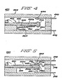
- FIG. 4 shows a switch 420 substantially identical to switch 20 ( Figures 1-3), with the exception of the construction of movable contact 442 and the electrical connections thereto.
- each movable contact 422 comprises a metal clip of generally circular cross-section clipped onto the end of its corresponding element finger 422a and spaced from metal layers 432 and 434.
- a flexible printed circuit board 460 is disposed in case 424 and includes a separate electrical conductor for making electrical connection between each movable contact clip 422 and a corresponding, separate pad 464 or conductor (not shown).
- a separate connection (not shown) is subsequently made to each pad 464, for example using a conductor similar to 48 of Figures 1-3, for making external connections to pads 464.
- switch 420 Operation of switch 420 is identical to that described for switch 20 ( Figures 1-3) above.
- the alternate construction of movable contacts 442 and the use of printed circuit board 460 permits the movable contacts to be fabricated independently from element 422 and easily assembled thereon during the subsequent assembly process.
- FIG. 5 shows a switch 520 substantially identical to switch 20 ( Figures 1-3), with the exception of the construction of a movable contact assembly 542.
- each movable contact assembly 542 comprises a pair of contacts 542a spaced from metal layers 532 and 534, respectively, by intermediately disposed layers 468 of insulating material. These metal contacts are connected by an electrical conductor 542b wrapped around the tip of element finger 522a and spaced from metal layers 536 and 538 and the conductive center layers of finger 522a (not shown).
- Flexible electrical conductor 546 is disposed in contact with movable contact assembly 542 for making external electrical connection thereto.
- switch 520 is substantially identical to that of matrix switch 20 ( Figures 1-3).
- the use of insulating layers 468 underneath contact pads 524a permits metal layers 532 and 534 to extend substantially to the tip of element fingers 522a, providing the element fingers with a stronger deflection force. Further, the thickness of insulating layers 468 between the layers of metallization and the metal pads can be varied to subsequently adjust the spacing between movable contacts 542a and stationary contacts 544.
- FIGS 6 and 6A illustrate a switch 620 substantially identical to switch 20 ( Figures 1-3), with the exception of the construction of electrical conductors 646. Like features are indicated by like reference numerals incremented by 600.
- electrical conductors 646 are plated on element fingers 622a (spaced from the metal layers thereon), anchor 626 and case surface 624a. Each electrical conductor 646 terminates in a respective pad 646a disposed on surface 624a of case 624. Subsequent electrical connections(not shown), for example in the form of conductors 648, are made to pads 646a to accommodate external electrical connections. Operation of switch 620 is substantially identical to that of switch 20.
- FIGS 7 and 7A show a switch 720 substantially identical to switch 20 ( Figures 1-3) with the exception of the construction of the movable and stationary contacts 742 and 744. Like features are indicated by like reference numerals incremented by 700. Various, previously described details of the matrix switch have been omitted from the drawing for the purpose of clearly illustrating the changed features.
- each element finger 722a supports a pair of separate movable contacts 742a,742b in the form of a pair of separate studs extending through the element finger.
- Each element finger 722a is shown with an optional bifurcation 780 proximate its tip extending vertically through the element finger between the movable contact pair.
- a separate pair of stationary contacts 744a and 744b is disposed on each of case surfaces 724a and 724b, opposite each pair of movable contacts 742a and 742b, respectively.
- switch 720 is substantially identical to that of switch 20 ( Figures 1-3) with the exception that each element finger 722a switches two separate movable contacts 742a and 742b into selective contact with two separate pairs of stationary contacts 744a and 744b.
- Switch 720 thus makes available twice as many switchable connections as switch 20 of Figures 1-3.
- Bifurcating cuts 780 permit movable contacts 742a and 742b to vary slightly in their deflected distance and make good electrical contact with the respective, opposing stationary contact 744a,744b. This bifurcated construction thus accommodates minor manufacturing deviations, for example in the relative thickness of the various contacts, which might otherwise interfere with the establishing of good mechanical and electrical connections.
- FIGS 8 and 8A also show an alternate embodiment of switch 20 ( Figures 1-3) wherein the drawings have been simplified to better illustrate the alternate construction of movable contacts 842a and 842b and stationary contacts 844a and 844b.
- each element finger 822a supports two separate, rectangularly shaped movable contacts 842a and 842b, one contact 842a being disposed on the top surface of each element finger, and one contact 842b being disposed on the bottom surface of each element finger (as viewed in Figures 8 and 8A).
- One pair of stationary contacts 844a is disposed on case surfaces 824b opposite each movable contact 842a.
- one pair of stationary contacts 844b is disposed on case surface 824a opposite each movable contact 842b. It will be understood that in the embodiments of the invention shown in the simplified drawings for Figures 7 and 8, the movable contacts are spaced or insulated from the layers of metal on the element fingers as in the previous embodiments described hereinabove.
- movable contacts 842a and 842b act to electrically bridge and thus short circuit the opposing pair of stationary contacts, thus establishing an electrical connection selectively between conductor pairs 844a or conductor pairs 844b.
- FIG 8B shows an alternate embodiment of element finger 822a and movable contacts 842a and 842b, and is enlarged to better illustrate detail.
- each finger 822a includes a vertically extending bifurcation 822d.
- Each movable contact comprises a generally U-shaped plate edging bifurcation 822d, spaced from the metal layers on the finger (only metal layer 832 being visible in Figure 8), and terminating in two pads 842c at the tip of the finger, one pad on each side of the bifurcation.
- Metallization layers 832 and 834 can optionally terminate short of bifurcation 822d, leaving the tip of element finger 822a, proximate the bifurcation, unpoled.
- a switch each of which uses a bimorph piezoelectric bender element in a compact, comb shaped configuration to provide separate control of multiple, closely spaced, switchable electrical contacts.
- the switch is light in weight, small in size, and can be constructed using known fabrication technologies. Precision semiconductor microcircuit fabrication techniques can be used to manufacture large quantities of these switches with reliable, repeatable, close-tolerance features.
- the nature of the switch provides a high degree of electrical isolation, and hence low cross-talk, between switched signals even at frequencies approaching the megahertz range.
- each embodiment of the switch has a low actuator power requirement, and comprises sturdy, reliable components.
- the exact nature of the contact construction and hence the switching operations can be tailored to specific operational and/or manufacturing requirements. Further, the inclusion of electronic circuit elements on the piezoelectric element and within the case provides a substantially self-contained unit with the attendant advantages of ease of installation and serviceability in a compact package.
- a switch constructed in accordance with the present invention could comprise, for example, a single element finger extending opposite of two or more fingers, or any other combination of oppositely extending fingers.
Landscapes
- Push-Button Switches (AREA)
- Micromachines (AREA)
- Oscillators With Electromechanical Resonators (AREA)
- Electrophonic Musical Instruments (AREA)
Applications Claiming Priority (2)
| Application Number | Priority Date | Filing Date | Title |
|---|---|---|---|
| US896792 | 1986-08-15 | ||
| US06/896,792 US4697118A (en) | 1986-08-15 | 1986-08-15 | Piezoelectric switch |
Publications (1)
| Publication Number | Publication Date |
|---|---|
| EP0257929A2 true EP0257929A2 (fr) | 1988-03-02 |
Family
ID=25406850
Family Applications (2)
| Application Number | Title | Priority Date | Filing Date |
|---|---|---|---|
| EP87307181A Withdrawn EP0257929A2 (fr) | 1986-08-15 | 1987-08-14 | Relais piézoélectrique |
| EP19870905842 Withdrawn EP0277224A4 (en) | 1986-08-15 | 1987-08-14 | Piezoelectric switch |
Family Applications After (1)
| Application Number | Title | Priority Date | Filing Date |
|---|---|---|---|
| EP19870905842 Withdrawn EP0277224A4 (en) | 1986-08-15 | 1987-08-14 | Piezoelectric switch |
Country Status (8)
| Country | Link |
|---|---|
| US (1) | US4697118A (fr) |
| EP (2) | EP0257929A2 (fr) |
| JP (2) | JPS6388727A (fr) |
| KR (2) | KR880003362A (fr) |
| AU (1) | AU594818B2 (fr) |
| CA (1) | CA1269129A (fr) |
| NO (1) | NO881588L (fr) |
| WO (1) | WO1988001438A1 (fr) |
Cited By (3)
| Publication number | Priority date | Publication date | Assignee | Title |
|---|---|---|---|---|
| GB2197128B (en) * | 1986-09-24 | 1990-02-07 | Gen Electric | Piezoelectric relay switching matrix |
| EP0455342A1 (fr) * | 1990-05-01 | 1991-11-06 | Ngk Insulators, Ltd. | Dispositif d'actionnement piézo-électrique/électrostrictif ayant au moins une couche piézo-électrique/électrostrictive |
| US8966731B2 (en) | 2007-03-26 | 2015-03-03 | Semiconductor Energy Laboratory Co., Ltd. | Method for manufacturing a switching element |
Families Citing this family (26)
| Publication number | Priority date | Publication date | Assignee | Title |
|---|---|---|---|---|
| US4742263A (en) * | 1986-08-15 | 1988-05-03 | Pacific Bell | Piezoelectric switch |
| US4868448A (en) * | 1986-09-24 | 1989-09-19 | General Electric Company | Piezoelectric relay switching matrix |
| US4819126A (en) * | 1988-05-19 | 1989-04-04 | Pacific Bell | Piezoelectic relay module to be utilized in an appliance or the like |
| US4893048A (en) * | 1988-10-03 | 1990-01-09 | General Electric Company | Multi-gap switch |
| US5149673A (en) * | 1989-02-21 | 1992-09-22 | Cornell Research Foundation, Inc. | Selective chemical vapor deposition of tungsten for microdynamic structures |
| US5072288A (en) * | 1989-02-21 | 1991-12-10 | Cornell Research Foundation, Inc. | Microdynamic release structure |
| DE69026765T2 (de) * | 1989-07-11 | 1996-10-24 | Ngk Insulators Ltd | Einen piezoelektrischen/elektrostriktiven Film enthaltende piezoelektrischer/elektrostriktiver Antrieb |
| DE69223096T2 (de) * | 1991-07-18 | 1998-05-28 | Ngk Insulators Ltd | Piezoelektrischer/elektrostriktiver Element mit einem keramischen Substrat aus stabilisiertem Zirkoniumdioxid |
| US5479042A (en) * | 1993-02-01 | 1995-12-26 | Brooktree Corporation | Micromachined relay and method of forming the relay |
| JP3432974B2 (ja) * | 1995-10-13 | 2003-08-04 | 日本碍子株式会社 | 圧電/電歪膜型素子 |
| US6265811B1 (en) * | 1996-11-29 | 2001-07-24 | Ngk Insulators, Ltd. | Ceramic element, method for producing ceramic element, display device, relay device and capacitor |
| US6060817A (en) * | 1998-04-06 | 2000-05-09 | Motorola, Inc. | Switching method using a frequency domain piezoelectric switch |
| US6359374B1 (en) | 1999-11-23 | 2002-03-19 | Mcnc | Miniature electrical relays using a piezoelectric thin film as an actuating element |
| US6836056B2 (en) | 2000-02-04 | 2004-12-28 | Viking Technologies, L.C. | Linear motor having piezo actuators |
| US6437226B2 (en) | 2000-03-07 | 2002-08-20 | Viking Technologies, Inc. | Method and system for automatically tuning a stringed instrument |
| US6548938B2 (en) | 2000-04-18 | 2003-04-15 | Viking Technologies, L.C. | Apparatus having a pair of opposing surfaces driven by a piezoelectric actuator |
| US6717332B2 (en) | 2000-04-18 | 2004-04-06 | Viking Technologies, L.C. | Apparatus having a support structure and actuator |
| US6759790B1 (en) | 2001-01-29 | 2004-07-06 | Viking Technologies, L.C. | Apparatus for moving folded-back arms having a pair of opposing surfaces in response to an electrical activation |
| US6879087B2 (en) | 2002-02-06 | 2005-04-12 | Viking Technologies, L.C. | Apparatus for moving a pair of opposing surfaces in response to an electrical activation |
| WO2004001871A2 (fr) * | 2002-06-21 | 2003-12-31 | Viking Technologies, L.C. | Moteur piezo-electrique monobloc |
| CA2521307C (fr) | 2003-04-04 | 2014-07-15 | Viking Technologies, L.C. | Appareil et processus d'optimisation du travail a partir d'un dispositif de commande materiel intelligent |
| KR101092536B1 (ko) * | 2005-11-30 | 2011-12-13 | 삼성전자주식회사 | 압전형 rf 멤스 소자 및 그 제조방법 |
| JP4714242B2 (ja) * | 2008-05-30 | 2011-06-29 | 株式会社アドバンテスト | バイモルフスイッチ、電子回路、及び電子回路製造方法 |
| US8250001B2 (en) | 2008-12-18 | 2012-08-21 | Motorola Mobility Llc | Increasing user input accuracy on a multifunctional electronic device |
| FR3022690B1 (fr) * | 2014-06-24 | 2016-07-22 | Commissariat Energie Atomique | Dispositif de connexion electrique comportant des elements de connexion a position commandable |
| US20160293829A1 (en) * | 2015-04-01 | 2016-10-06 | 19th Space Electronics | Piezoelectric switch with lateral moving beams |
Family Cites Families (26)
| Publication number | Priority date | Publication date | Assignee | Title |
|---|---|---|---|---|
| NL51407C (fr) * | 1937-03-16 | |||
| US2203332A (en) * | 1938-09-09 | 1940-06-04 | Bell Telephone Labor Inc | Piezoelectric device |
| US2835761A (en) * | 1953-05-25 | 1958-05-20 | Electric Machinery Mfg Co | Electrostrictive ceramic actuator |
| DE1096095B (de) * | 1957-08-22 | 1960-12-29 | Siemens Ag | Piezoelektrischer Biegeschwinger aus polykristallinem, dielektrischem Werkstoff |
| GB1096824A (en) * | 1964-03-26 | 1967-12-29 | Plessey Uk Ltd | Improvements in electric relays |
| US3646413A (en) * | 1970-09-25 | 1972-02-29 | Avco Corp | Piezoelectric-driven variable capacitor |
| US4093883A (en) * | 1975-06-23 | 1978-06-06 | Yujiro Yamamoto | Piezoelectric multimorph switches |
| JPS5239391A (en) * | 1975-09-25 | 1977-03-26 | Citizen Watch Co Ltd | Composite vibrator for watches |
| JPS5260005A (en) * | 1975-11-12 | 1977-05-18 | Fujitsu Ltd | Piezoelectric type switch matrix |
| US4112279A (en) * | 1977-09-02 | 1978-09-05 | Bell Telephone Laboratories, Incorporated | Piezoelectric relay construction |
| DE2811558A1 (de) * | 1978-03-16 | 1979-09-20 | Siemens Ag | Piezoelektrisches koppelfeld |
| JPS5521679A (en) * | 1978-08-04 | 1980-02-15 | Seiko Epson Corp | Crystal oscillator of composite mode h type |
| US4295172A (en) * | 1978-11-10 | 1981-10-13 | Matsushita Electric Industrial Co., Ltd. | Rotary magnetic head apparatus |
| US4368402A (en) * | 1980-07-02 | 1983-01-11 | Fuji Electrochemical Co., Ltd. | H-Type ceramic resonator |
| US4362407A (en) * | 1981-09-08 | 1982-12-07 | Piezo Electric Products, Inc. | Piezoelectric printer and piezoelectric multilam actuator used therein |
| US4450375A (en) * | 1982-11-12 | 1984-05-22 | Kiwi Coders Corporation | Piezoelectric fluid control device |
| GB2144546B (en) * | 1983-08-04 | 1987-05-28 | Standard Telephones Cables Ltd | Surface acoustic wave accelerometer |
| JPS6046636U (ja) * | 1983-09-05 | 1985-04-02 | オムロン株式会社 | 多極リレ− |
| JPS6116867A (ja) * | 1984-05-29 | 1986-01-24 | Yasuhiko Ogawa | 櫛型の圧電駆動装置 |
| US4553061A (en) * | 1984-06-11 | 1985-11-12 | General Electric Company | Piezoelectric bimorph driven direct current latching relay |
| US4538087A (en) * | 1984-06-11 | 1985-08-27 | General Electric Company | Alternating current driven piezoelectric latching relay and method of operation |
| US4678957A (en) * | 1986-06-24 | 1987-07-07 | General Electric Company | Piezoelectric ceramic switching devices and systems and methods of making the same |
| US4689517A (en) * | 1984-12-21 | 1987-08-25 | General Electric Company | Advanced piezoceramic power switching devices employing protective gastight enclosure and method of manufacture |
| US4670682A (en) * | 1984-12-21 | 1987-06-02 | General Electric Company | Piezoelectric ceramic switching devices and systems and method of making the same |
| US4714847A (en) * | 1984-12-21 | 1987-12-22 | General Electric Company | Advanced piezoeceramic power switching devices employing protective gastight enclosure and method of manufacture |
| SE502098C2 (sv) * | 1986-09-24 | 1995-08-14 | Gen Electric | Piezoelektrisk omkopplingsmatris |
-
1986
- 1986-08-15 US US06/896,792 patent/US4697118A/en not_active Expired - Lifetime
-
1987
- 1987-08-07 KR KR1019870008666A patent/KR880003362A/ko not_active Withdrawn
- 1987-08-12 JP JP62200140A patent/JPS6388727A/ja active Pending
- 1987-08-14 JP JP62505267A patent/JPH01501186A/ja active Pending
- 1987-08-14 EP EP87307181A patent/EP0257929A2/fr not_active Withdrawn
- 1987-08-14 AU AU79116/87A patent/AU594818B2/en not_active Ceased
- 1987-08-14 CA CA000544605A patent/CA1269129A/fr not_active Expired - Lifetime
- 1987-08-14 WO PCT/US1987/002029 patent/WO1988001438A1/fr not_active Ceased
- 1987-08-14 KR KR1019880700400A patent/KR950009641B1/ko not_active Expired - Lifetime
- 1987-08-14 EP EP19870905842 patent/EP0277224A4/en not_active Withdrawn
-
1988
- 1988-04-13 NO NO881588A patent/NO881588L/no unknown
Cited By (4)
| Publication number | Priority date | Publication date | Assignee | Title |
|---|---|---|---|---|
| GB2197128B (en) * | 1986-09-24 | 1990-02-07 | Gen Electric | Piezoelectric relay switching matrix |
| EP0455342A1 (fr) * | 1990-05-01 | 1991-11-06 | Ngk Insulators, Ltd. | Dispositif d'actionnement piézo-électrique/électrostrictif ayant au moins une couche piézo-électrique/électrostrictive |
| US5126615A (en) * | 1990-05-01 | 1992-06-30 | Ngk Insulators, Ltd. | Piezoelectric/electrostrictive actuator having at least one piezoelectric/electrostrictive film |
| US8966731B2 (en) | 2007-03-26 | 2015-03-03 | Semiconductor Energy Laboratory Co., Ltd. | Method for manufacturing a switching element |
Also Published As
| Publication number | Publication date |
|---|---|
| CA1269129A (fr) | 1990-05-15 |
| JPS6388727A (ja) | 1988-04-19 |
| KR880003362A (ko) | 1988-05-16 |
| NO881588L (no) | 1988-06-15 |
| NO881588D0 (no) | 1988-04-13 |
| AU7911687A (en) | 1988-03-08 |
| EP0277224A1 (fr) | 1988-08-10 |
| US4697118A (en) | 1987-09-29 |
| WO1988001438A1 (fr) | 1988-02-25 |
| JPH01501186A (ja) | 1989-04-20 |
| KR950009641B1 (ko) | 1995-08-25 |
| AU594818B2 (en) | 1990-03-15 |
| KR880701976A (ko) | 1988-11-07 |
| EP0277224A4 (en) | 1990-09-26 |
Similar Documents
| Publication | Publication Date | Title |
|---|---|---|
| US4742263A (en) | Piezoelectric switch | |
| US4697118A (en) | Piezoelectric switch | |
| US4819126A (en) | Piezoelectic relay module to be utilized in an appliance or the like | |
| US7027284B2 (en) | Variable capacitance element | |
| JP3119255B2 (ja) | マイクロマシンスイッチおよびその製造方法 | |
| US6153839A (en) | Micromechanical switching devices | |
| US6084281A (en) | Planar magnetic motor and magnetic microactuator comprising a motor of this type | |
| JP3890952B2 (ja) | 容量可変型キャパシタ装置 | |
| US4112279A (en) | Piezoelectric relay construction | |
| US20020140533A1 (en) | Method of producing an integrated type microswitch | |
| US4564832A (en) | Membrane keyboard having key closure retention | |
| US4868448A (en) | Piezoelectric relay switching matrix | |
| US20030080650A1 (en) | Longitudinal piezoelectric optical latching relay | |
| JP4386767B2 (ja) | 高分子アクチュエータを用いた電気素子 | |
| US20060091983A1 (en) | Electrostatic microswitch for low-voltage-actuation component | |
| KR20070014589A (ko) | 수직 콤 액츄에이터 알에프 멤스 스위치 | |
| WO1989007345A1 (fr) | Element de relais piezo-electrique ameliore et son procede d'excitation | |
| JP3805644B2 (ja) | 圧電アクチュエータ | |
| JP4804546B2 (ja) | マイクロリレー | |
| JP3636022B2 (ja) | マイクロマシンスイッチ | |
| JP2000348595A (ja) | マイクロマシンスイッチおよびその製造方法 | |
| KR100493532B1 (ko) | 정전식 양방향 미세기전 액추에이터 | |
| US20040201439A1 (en) | Mesoscale mems switch apparatus and method | |
| JPH11204013A (ja) | 静電型可動接点素子及び論理演算装置 | |
| KR20060004669A (ko) | 스위치 |
Legal Events
| Date | Code | Title | Description |
|---|---|---|---|
| PUAI | Public reference made under article 153(3) epc to a published international application that has entered the european phase |
Free format text: ORIGINAL CODE: 0009012 |
|
| AK | Designated contracting states |
Kind code of ref document: A2 Designated state(s): DE FR GB |
|
| STAA | Information on the status of an ep patent application or granted ep patent |
Free format text: STATUS: THE APPLICATION HAS BEEN WITHDRAWN |
|
| 18W | Application withdrawn |
Withdrawal date: 19890904 |
|
| R18W | Application withdrawn (corrected) |
Effective date: 19890904 |
|
| RIN1 | Information on inventor provided before grant (corrected) |
Inventor name: KORNRUMPF, WILLIAM PAUL Inventor name: ADLER, MICHAEL STUART Inventor name: HARNDEN, JOHN DAVIS, JR. Inventor name: KOHL, JAMES ELWOOD |