EP0258042B1 - Circuit d'asservissement de phase à recouvrement rapide de stabilité - Google Patents
Circuit d'asservissement de phase à recouvrement rapide de stabilité Download PDFInfo
- Publication number
- EP0258042B1 EP0258042B1 EP87307526A EP87307526A EP0258042B1 EP 0258042 B1 EP0258042 B1 EP 0258042B1 EP 87307526 A EP87307526 A EP 87307526A EP 87307526 A EP87307526 A EP 87307526A EP 0258042 B1 EP0258042 B1 EP 0258042B1
- Authority
- EP
- European Patent Office
- Prior art keywords
- phase
- signal
- pulse
- voltage
- reference signal
- Prior art date
- Legal status (The legal status is an assumption and is not a legal conclusion. Google has not performed a legal analysis and makes no representation as to the accuracy of the status listed.)
- Expired - Lifetime
Links
Images







Classifications
-
- H—ELECTRICITY
- H04—ELECTRIC COMMUNICATION TECHNIQUE
- H04N—PICTORIAL COMMUNICATION, e.g. TELEVISION
- H04N5/00—Details of television systems
- H04N5/04—Synchronising
- H04N5/12—Devices in which the synchronising signals are only operative if a phase difference occurs between synchronising and synchronised scanning devices, e.g. flywheel synchronising
- H04N5/126—Devices in which the synchronising signals are only operative if a phase difference occurs between synchronising and synchronised scanning devices, e.g. flywheel synchronising whereby the synchronisation signal indirectly commands a frequency generator
-
- H—ELECTRICITY
- H03—ELECTRONIC CIRCUITRY
- H03L—AUTOMATIC CONTROL, STARTING, SYNCHRONISATION OR STABILISATION OF GENERATORS OF ELECTRONIC OSCILLATIONS OR PULSES
- H03L7/00—Automatic control of frequency or phase; Synchronisation
- H03L7/06—Automatic control of frequency or phase; Synchronisation using a reference signal applied to a frequency- or phase-locked loop
- H03L7/16—Indirect frequency synthesis, i.e. generating a desired one of a number of predetermined frequencies using a frequency- or phase-locked loop
- H03L7/18—Indirect frequency synthesis, i.e. generating a desired one of a number of predetermined frequencies using a frequency- or phase-locked loop using a frequency divider or counter in the loop
- H03L7/197—Indirect frequency synthesis, i.e. generating a desired one of a number of predetermined frequencies using a frequency- or phase-locked loop using a frequency divider or counter in the loop a time difference being used for locking the loop, the counter counting between numbers which are variable in time or the frequency divider dividing by a factor variable in time, e.g. for obtaining fractional frequency division
- H03L7/199—Indirect frequency synthesis, i.e. generating a desired one of a number of predetermined frequencies using a frequency- or phase-locked loop using a frequency divider or counter in the loop a time difference being used for locking the loop, the counter counting between numbers which are variable in time or the frequency divider dividing by a factor variable in time, e.g. for obtaining fractional frequency division with reset of the frequency divider or the counter, e.g. for assuring initial synchronisation
-
- H—ELECTRICITY
- H04—ELECTRIC COMMUNICATION TECHNIQUE
- H04N—PICTORIAL COMMUNICATION, e.g. TELEVISION
- H04N5/00—Details of television systems
- H04N5/76—Television signal recording
- H04N5/91—Television signal processing therefor
- H04N5/93—Regeneration of the television signal or of selected parts thereof
- H04N5/95—Time-base error compensation
- H04N5/956—Time-base error compensation by using a digital memory with independent write-in and read-out clock generators
Definitions
- This invention relates to a phase locked loop (PLL) circuit, and more particularly to a PLL circuit applied with an input signal which would often cause discontinuous changes in phase.
- PLL phase locked loop
- a digital signal processing circuit such as a time-base collector (TBC) in a video tape recorder (VTR) uses a memory for temporarily storing a digital video signal as shown in FIG. 1.
- TBC time-base collector
- VTR video tape recorder
- a digital video signal is written into a memory 51 in response to a write clock and the stored digital video signal is read out from the memory 51 in response to a read clock.
- the address of the memory 51 is reset periodically, for example at intervals of horizontal scanning period (H), by a reset signal.
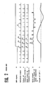
- a reference signal d which is a periodic pulse train as shown in FIG. 2 produced from the horizontal synchronizing signal or the burst signal of the video signal reproduced via a pair of rotary heads from a recording tape.
- the write clock is generated from the reference signal by a PLL circuit 50 comprising a phase comparator 2, a low-pass filter (LPF) 3, a voltage controlled oscillator (VCO) 4 and a frequency divider 5.
- the PLL circuit 50 operates so that the phase of the output signal e of the frequency divider 5 is locked to the phase of the reference signal d.
- the response speed of the PLL circuit 50 which is determined by the time constant of the LPF 3 cannot be made too short so that the PLL circuit 50 does not respond to a noise.
- the PLL circuit 50 arranged as above cannot immediately recover the stable state when the reference signal d causes a discontinuous change in phase. Since the video signal recorded on the recorded tape is reproduced via a pair of alternately switched heads, there would be caused a discontinuity of the reproduced signal, resulting in a sudden change of the phase of the reference signal.
- HSW is the head switching signal for periodically changing over the pair of heads, and the reference signal causes a discontinuous phasechange between pulses d1 and d2.
- the phase comparator 2 generates an error signal g corresponding to the phase difference between the reference signal d and the output signal e of the frequency divider 5.
- the frequency divider 5 resets itself by the reset signal f synchronized with the signal e.
- the error signal g is converted by the LPF 3 to a gradually changing voltage signal h. Therefore, it takes a fairly long time (about 10H in the case of Fig. 2) for the PLL circuit 50 to recover the stable state in which the phase of the output signal of the frequency divider 5 is locked to the phase of the reference signal after the discontinuous phase change.
- a phase locked loop circuit is disclosed in DE-A-2,716,813 as comprising: a voltage-controlled oscillator oscillating at a frequency corresponding to a voltage applied thereto; a frequency divider for dividing the oscillation frequency of the voltage-controlled oscillator; a phase comparator for comparing phases of a reference signal inputted to the phase locked loop circuit and an output signal of the frequency divider; a low-pass filter for converting a phase comparison result of the phase comparator to a voltage for controlling the voltage-controlled oscillator; first control means responsive to a discontinuous phase change of the reference signal for preventing a phase change of the reference signal from being transmitted through the low-pass filter to the voltage controlled oscillator during a predetermined period; and second control means responsive to the discontinuous phase change of the reference signal for forcedly pulling-in the phase of the phase locked loop circuit so that the phase of the output signal of the frequency divider is locked to a new phase of the reference signal after the discontinuous change during a predetermined period.
- US-A-4,005,479 discloses a phase locked loop circuit comprising a means for resetting a frequency divider of the loop circuit in response to a pulse of the new reference signal whereby to forcedly lock the phase of the output signal of the frequency divider to the new phase of the reference signal.
- an object of the present invention is to provide a PLL circuit which is capable of recovering stability when an input signal of the PLL circuit causes a discontinous change in phase.
- a PLL circuit comprises: a voltage-controlled oscillator oscillating at a frequency corresponding to a voltage applied thereto; a frequency divider for dividing the oscillation frequency of the voltage-controlled oscillator; a phase comparator for comparing phases of a reference signal inputted to the phase locked loop circuit and an output signal of the frequency divider; a low-pass filter for converting a phase comparison result of the phase comparator to a voltage for controlling the voltage-controlled oscillator; first control means responsive to a discontinuous phase change of the reference signal for preventing a phase change of the reference signal from being transmitted through the low-pass filter to the voltage controlled oscillator during a predetermined period; and second control means responsive to the discontinuous phase change of the reference signal for forcedly pulling-in the phase of the phase locked loop circuit so that the phase of the output signal of the frequency divider is locked to a new phase of the reference signal after the discontinuous change during a predetermined period; characterised in that said first control means comprises: a first pulse generator responsive to the discontinu
- a first control means inhibits the phase comparison operation of the phase comparator, and a second control means resets the frequency divider by a pulse of the reference signal after the discontinuous phase change.
- the first control means disconnects the low-pass filter from the phase comparator, and the second control means generates a voltage signal corresponding to the discontinuous phase change of the reference signal and applies this voltage signal to the voltage-controlled oscillator for changing the oscillation frequency so that the phase of the output signal of the frequency divider becomes closer or equal to the phase of the reference signal after the discontinuous phase change.
- the PLL circuit Since the discontinuous phase change of the reference signal is not transmitted through the low-pass filter to the voltage-controlled oscillator, no long time unstable state due to the time constant of the low-pass filter is caused. At the same time, the PLL circuit is forcedly locked to the new phase of the reference signal after the discontinuous phase change during a short period. Thus, the PLL circuit can recover its stable state quickly after the discontinuous phase change of the reference signal.
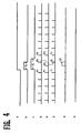
- FIG. 3 shows an arrangement of PLL circuit and FIGs. 4 and 5 show signal waveform chart for explaining the operation of the PLL circuit in FIG. 3.
- a reference signal inputted to the PLL circuit through an input terminal 1 is a periodic pulse train having a period of H (horizontal scanning period) produced from the horizontal synchronizing signal or the burst signal of a video signal reproduced from a recording tape via a pair of rotary heads.
- a voltage controlled oscillator (VCO) 4 generates a predetermined high frequency signal which is higher in frequency than and equal in phase to the reference signal when an output signal h of a low-pass filter (LPF) 3 inputted to the VCO 4 is kept constant in level. This high frequency signal is outputted through an output terminal 11 as an output signal of the PLL circuit.
- LPF low-pass filter
- the high frequency signal from the VCO 4 is on the other hand divided in frequency by a frequency divider 5 to be equal in frequency to the reference signal as shown as an output signal e of the frequency divider 5.
- the frequency divider 5 generates also a reset signal which is synchronized with the output signal e for resetting itself.
- a phase comparator 2 compares the phases of the reference signal d and the output signal e of the frequency divider 5.
- An output signal g of the phase comparator 2 applied to the LPF 3 is 0 when the phases of the reference signal d and the output signal e of the frequency divider 5 are equal to each other, i.e., when the PLL circuit is in the phase-locked state.
- the pair of rotary heads are periodically alternately selected by a head switching signal (HSW signal). Since a discontinuity of the reproduced video signal and the resultant discontinuous phase change of the reference signal d would occur at each switching timing of the pair of rotary head, the HSW signal can be regarded as a discontinuous phase change informing signal for informing an occurrence of discontinuous phase change of the reference signal d.
- the HSW signal referred to by the symbol a is inputted to the PLL circuit through an additional input terminal 10.
- a transition detector 12 produces a pulse in response to each transition of the level (from LOW to HIGH or from HIGH to LOW) of the HSW signal a.
- a monostable multivibrator (MM) 8 produces a pulse b having a duration T1 in response to the output pulse of the transition detector 12.
- the pulse b is applied to a switch 7.
- the switch 7 normally connects its common terminal C to its first terminal A so that the reset signal from the frequency divider 7 becomes a reset signal f applied to a RESET terminal of the frequency divider 5.
- a second terminal B of the switch 7 is connected through a delay circuit 6 to the input terminal 1.
- the switch 7, when the pulse b is applied thereto, connects the common terminal C to the second terminal B so that the reference signal adjusted in timing by the delay circuit 6 becomes the reset signal f during the duration T1 of the pulse B.
- the delay circuit 6 is not always necessary, but may be removed if it is not necessary to adjust the timing of the reference signal applied as the reset signal f to the frequency divider 5.
- a monostable multivibrator (MM) 9 produces a pulse c having a duration T2 in response to the output pulse of the transition detector 12.
- the pulse c is applied to an INHIBIT terminal of the phase comparator 2 to inhibit the phase comparison operation of the phase comparator 2 during the duration T2 of the pulse c. Therefore, the phase change information of the reference signal is not transferred to the VCO 4 during the duration T2 of the pulse c.
- the output signal e of the frequency divider 5 (e1, for example) is phase-locked to the reference signal d (d1, for example), and the reset signal f (f1, for example) is synchronized with the signal e.
- the phase of the reference signal d is discontinuously delayed as shown by d2, so that a large phase difference is caused between the reference signal d2 and the output signal e2 of the frequency divider 5.
- the phase comparator 2 were active, the phase comparator 2 would produce an error signal g1 corresponding to the phase error between d2 and e2. However, since the operation of the phase comparator 2 is inhibited by the pulse c as described above, no error signal is produced by the phase comparator 2.
- the reference signal d2 becomes the reset signal f2 for resetting the frequency divider 5.
- the next pulse e3 of the output signal e of the frequency divider 5 becomes equal to, or locked to, the reference signal d3.
- Both of the pulses b and c have been ended before the occurrence of the pulse d3 of the reference signal, so that the PLL circuit has started its normal operation with a phase-locked state to the new phase of the reference signal.
- the reset signal is again synchronized with the signal e as shown by f3.
- FIG. 5 shows the operation of the PLL circuit in FIG.3 in the case that the phase of the reference signal e is discontinuously advanced.
- FIG. 5 may be easily understood from the above description. Thus, the description of FIG. 5 is omitted.
- the operation of the phase comparator is inhibited during a predetermined time so that the discontinuous phase change information is not transferred through the LPF to the VCO.
- the frequency divider is forcedly reset by the reference signal after the discontinuous phase change so that the output signal of the frequency divider is quickly phase-locked to the reference signal after the discontinuous phase change. Accordingly, the PLL circuit can quickly recover the stable phase-locked state even when a discontinuous phase change of the reference signal is caused.
- the arrangement shown in FIG. 3 uses different monostable multivibrators 8, 9 for producing the pulses b, c having different durations from each other.
- a single monostable multivibrator may be used for producing a pulse having a predetermined duration which is applied to both the phase comparator and the switch.
- other various pulse generating circuits may be used instead of multivibrator.
- the multivibrator may be replaced by a flip-flop circuit which is set by the output pulse of the transition detector 12 and reset by the reset pulse f2 or by a pulse obtained by delaying the reset pulse f2 for a predetermined time shorter than the period of the reference signal.
- FIG. 6 shows an embodiment of PLL circuit according to the invention used in a VTR.
- the reference signal inputted through the input terminal 1, the HSW signal inputted through the input terminal 10, and the configuration and function of each of the phase comparator 2, LPF 3, VCO 4, frequency divider 5, transition detector 12 and MMs 8, 9 are the same as those of the FIG. 3 embodiment.
- the structural elements peculiar to the PLL circuit in FIG. 6 are a switch 16 connected between the phase comparator 2 and the LPF 3, an adder 15 connected between the LPF 3 and the VCO 4, and a voltage generator 13 and a switch 14 which are connected between the phase comparator 2 and the adder 15.
- the switch 16 is normally closed to pass the output signal of the phase comparator 2 to the LPF 3.
- the switch 16 is opened in response to the output pulse b of the MM 8 so that the output signal of the phase comparator is not transmitted to the LPF 3 during the duration T1 of the pulse b.
- the voltage generator 13 generates a voltage signal corresponding to the output signal of the phase comparator 2.
- the switch 14 is normally opened, but is closed in response to the output pulse c of the MM 9 so as to pass the voltage signal from the voltage generator 13 to the adder 15 during the duration T2 of the pulse c.
- the adder 15 adds the output signals of the LPF 3 and the switch 14, and applies the added result to the VCO 4.
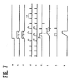
- FIG. 7 which shows a waveform chart for explaining the operation of the PLL circuit in FIG. 6, a discontinuous phase change is caused between pulses d1 and d2 of the reference signal d.
- the phase comparator 2 outputs an error signal g1 which is a pulse having a duration corresponding to the phase difference between the reference signal d2 and the output signal e2 of the frequency divider 5.
- the error signal g1 is not transmitted to the LPF 3 as shown in the broken line pulse waveform in FIG. 7.
- the output signal of the LPF 3 does not follow the discontinuous phase change of the reference signal d.
- the discontinuous phase change of the reference signal d is not transmitted through the LPF 3 to the VCO 4.
- the voltage generator 13 generates a voltage signal i having a level v1 corresponding to the pulse width of the error signal g1.
- An exemplary configuration of the voltage generator 13 is shown in FIG. 8.
- a circuit composed of resistors 21, 24, 26, a diode 22, a capacitor 23 and a buffer 25 generates a positive voltage corresponding to the pulse with of the positive error pulse signal.
- a circuit composed of resistors 27, 30, 32, a diode 28, a capacitor 29 and a buffer 31 generates a negative voltage corresponding to the pulse width of the negative error pulse signal.
- the voltage generator 13 may generate a constant-voltage pulse having a duration corresponding to the pulse width of the error signal produced by the phase comparator 2.
- the necessary function of the voltage generator 13 is to generate such a voltage signal that the integrated value thereof during the time T1 (which is the duration of the pulse c) in which the switch 14 is closed corresponds to the pulse width of the error signal produced by the phase comparator 2.
- the voltage signal i generated by the voltage generator 2 is applied through the switch 14 to the adder 15. Since the output signal of the LPF 3 is kept unchanged, the voltage signal i becomes a change of voltage signal k applied to the VCO 4. In response to the rapid change of the voltage signal k, the VCO 4 rapidly changes (decreases in the case of FIG. 7) its oscillation frequency so that the phase of the output signal e of the frequency divider 5 rapidly becomes close to that of the reference signal. That is, the pulse e3 next to the pulse e2 of the output signal e of the frequency divider 5 becomes close in phase to the pulse d3 next to the pulse d2 of the reference signal. Since the phase difference between the pulse d3 and the pulse e3 is now very small, the PLL circuit can be immediately brought into the phase-locked state by its normal control loop.
- the switch for normally connecting the phase comparator and the LPF is opened during a predetermined time so that the discontinuous phase change information is not transmitted through the LPF to the VCO.
- the voltage generator generates rapidly a voltage signal corresponding to the pulse width of the error signal produced by the phase comparator, and the generated voltage signal is applied to the VCO to forcedly change the oscillation frequency of the VCO so that the output signal of the frequency divider is quickly phase-locked to the reference signal after the discontinuous phase change of the reference signal. Accordingly, the PLL circuit can quickly recover the stable phase-locked state even when a discontinuous phase change of the reference signal is caused.
- the two MMs 8, 9 may be replaced by a single monostable multivibrator which is responsive to the output pulse of the transition detector 12 for producing a pulse having a predetermined duration which is applied to both the switches 16, 14.
- the multivibrator may be replaced by a flip-flop circuit which is set by the output pulse of the transition detector 12 and reset by a pulse obtained by delaying the pulse d2 of the reference signal for a predetermined time shorter than the period of the reference signal.
- the HSW signal is used as the discontinuous plase change informing signal for controlling the PLL circuit in the arrangements shown in FIGs. 3 and 6.
- the vertical synchronizing signal contained in the reproduced video signal may be used as the discontinuous plase change informing signal because the transition timing of the HSW is generally adjacent to the vertical synchronizing signal occurrence timing.
- each of the PULL circuits shown in FIGs. 3 and 6 uses the HSW signal as the control signal for controlling the PLL circuit to recover the stable state.
- the PLL circuit would be used in other apparatus in which the signal like the HSW signal is not available.
- FIG. 9 shows a PLL circuit which is obtained by modifying the FIG. 3 arrangement such that the input terminal 9 and the transition detector 12 are removed and a phase change detector 40 is connected between the phase comparator 2 and the MMs 8, 9.
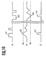
- FIG. 10 shows a waveform chart for explaining the operation of the phase change detector 40.
- the phase change detector 40 is responsive to a large phase change of the reference signal d for producing a pulse which triggers the MMs 8, 9.
- the phase change detector 40 outputs the pulse for triggering the MMs 8, 9 so that the PLL circuit recovers its stable state in the manner as described above in connection with the embodiment shown in FIG. 3.
- the signal A inputted to a low-pass filter (LPF) 41 is the output signal of the phase comparator 2.
- the phase comparator 2 When the phase comparator 2 outputs a positive pulse A1 having a wider pulse width than the predetermined pulse width, the output signal B of the LPF 41 becomes higher than an upper threshold level Va as shown by B1.
- a level comparator 42 produces a pulse C1 for triggering the MMs 8, 9.
- the phase comparator 2 outputs a negative pulse A2 having a wider pulse width than the predetermined pulse width
- the output signal B of the LPF 41 becomes lower than a lower threshold level Vb as shown by B2.
- a level comparator 43 produces a pulse C2 for triggering the MMs 8, 9.
- the pulse produced by the level comparator 42 or 43 is applied through an OR gate 44, as the pulse signal C, to the MMs 8, 9.
- the same modification can be applied to the FIG. 6 embodiment as shown in FIG. 11.
- the phase change detector 40 in FIG. 11 has the same configuration as that shown in FIG. 9, and is responsive to a large phase change of the reference signal for producing a pulse which triggers the MMs 8, 9 so that the PLL circuit recovers its stable state in the manner as described in connection with the FIG. 6 embodiment.
Landscapes
- Engineering & Computer Science (AREA)
- Multimedia (AREA)
- Signal Processing (AREA)
- Stabilization Of Oscillater, Synchronisation, Frequency Synthesizers (AREA)
Claims (1)
- Circuit de boucle à verrouillage de phase comprenant :
un oscillateur commandé en tension (4) qui oscille à une fréquence correspondant à une tension qui lui est appliquée ;
un diviseur de fréquence (5) pour diviser la fréquence d'oscillation de l'oscillateur commandé en tension ;
un comparateur de phase (2) pour comparer les phases d'un signal de référence entré sur le circuit de boucle à verrouillage de phase et d'un signal de sortie du diviseur de fréquence ;
un filtre passe-bas (3) pour convertir un résultat de comparaison de phase du comparateur de phase en une tension pour commander l'oscillateur commandé en tension ;
un premier moyen de commande (8, 16) sensible à une variation de phase discontinue du signal de référence pour empêcher qu'une variation de phase du signal de référence ne soit transmise au travers du filtre passe-bas à l'oscillateur commandé en tension pendant une période prédéterminée ; et
un second moyen de commande (9, 13, 14, 15) sensible à la variation de phase discontinue du signal de référence pour exciter de manière forcée la phase du circuit de boucle à verrouillage de phase de telle sorte que la phase du signal de sortie du diviseur de fréquence soit verrouillée sur une nouvelle phase du signal de référence après la variation discontinue pendant une période prédéterminée,
caractérisé en ce que ledit premier moyen de commande (8, 16) comprend : un premier générateur d'impulsion (8) sensible à la variation de phase discontinue du signal de référence pour générer une première impulsion présentant une durée prédéterminée ; et un premier commutateur (16) sensible à la première impulsion pour déconnecter le filtre passe-bas (3) du comparateur de phase (2) pendant la durée prédéterminée de la première impulsion ; et
ledit second moyen de commande (9, 13, 14, 15) comprend : un second générateur d'impulsion (9) sensible à la variation de phase discontinue du signal de référence pour générer une seconde impulsion présentant une durée prédéterminée ; un générateur de tension (13) pour générer un signal de tension correspondant à la variation de phase discontinue du signal de référence ; un second commutateur (14) sensible à la seconde impulsion pour laisser passer le signal de tension généré par le générateur de tension pendant la durée prédéterminée de la seconde impulsion ; et un additionneur de tension (15) pour additionner des tensions de sortie en provenance du filtre passe-bas et du second commutateur et pour appliquer une tension additionnée à l'oscillateur commandé en tension (4) afin de modifier de manière forcée la fréquence d'oscillation de telle sorte que la phase du signal de sortie du diviseur de fréquence (5) devienne verrouillée sur la nouvelle phase du signal de référence.
Applications Claiming Priority (6)
| Application Number | Priority Date | Filing Date | Title |
|---|---|---|---|
| JP61199640A JPS6356083A (ja) | 1986-08-26 | 1986-08-26 | 映像信号記録再生装置 |
| JP199640/86 | 1986-08-26 | ||
| JP61224458A JPS6379277A (ja) | 1986-09-22 | 1986-09-22 | 信号処理回路 |
| JP224458/86 | 1986-09-22 | ||
| JP61224457A JPS6379276A (ja) | 1986-09-22 | 1986-09-22 | 信号処理回路 |
| JP224457/86 | 1986-09-22 |
Publications (3)
| Publication Number | Publication Date |
|---|---|
| EP0258042A2 EP0258042A2 (fr) | 1988-03-02 |
| EP0258042A3 EP0258042A3 (en) | 1989-10-04 |
| EP0258042B1 true EP0258042B1 (fr) | 1994-04-06 |
Family
ID=27327675
Family Applications (1)
| Application Number | Title | Priority Date | Filing Date |
|---|---|---|---|
| EP87307526A Expired - Lifetime EP0258042B1 (fr) | 1986-08-26 | 1987-08-25 | Circuit d'asservissement de phase à recouvrement rapide de stabilité |
Country Status (3)
| Country | Link |
|---|---|
| US (1) | US4812783A (fr) |
| EP (1) | EP0258042B1 (fr) |
| DE (1) | DE3789528T2 (fr) |
Families Citing this family (43)
| Publication number | Priority date | Publication date | Assignee | Title |
|---|---|---|---|---|
| CA1290407C (fr) * | 1986-12-23 | 1991-10-08 | Shigeki Saito | Synthetiseur de frequence |
| JPH071423B2 (ja) * | 1988-12-20 | 1995-01-11 | 株式会社山下電子設計 | パルス発生回路 |
| JPH02211783A (ja) * | 1989-02-13 | 1990-08-23 | Toshiba Corp | 音声多重信号エンコーダ回路 |
| JP2975607B2 (ja) * | 1989-03-16 | 1999-11-10 | 三洋電機株式会社 | Afc回路 |
| US7382929B2 (en) * | 1989-05-22 | 2008-06-03 | Pixel Instruments Corporation | Spatial scan replication circuit |
| JPH0732389B2 (ja) * | 1989-09-22 | 1995-04-10 | 日本電気株式会社 | クロツクジツタ抑圧回路 |
| US5745314A (en) * | 1989-09-27 | 1998-04-28 | Canon Kabushiki Kaisha | Clock generating circuit by using the phase difference between a burst signal and the oscillation signal |
| JPH03114391A (ja) * | 1989-09-28 | 1991-05-15 | Toshiba Corp | フィルタ自動調整回路 |
| US5059925A (en) * | 1990-09-28 | 1991-10-22 | Stratacom, Inc. | Method and apparatus for transparently switching clock sources |
| GB9113922D0 (en) * | 1991-06-27 | 1991-08-14 | Thomson Consumer Electronics | Television sync disable circuit |
| JPH05207326A (ja) * | 1992-01-28 | 1993-08-13 | Matsushita Electric Ind Co Ltd | 水平圧縮pll回路 |
| EP0555569B1 (fr) * | 1992-02-11 | 1997-01-08 | International Business Machines Corporation | Dispositif de traitement de signal |
| US5610560A (en) * | 1993-04-20 | 1997-03-11 | Rca Thomson Licensing Corporation | Oscillator with switched reactive elements |
| US5574406A (en) * | 1993-04-20 | 1996-11-12 | Rca Thomson Licensing Corporation | Phase lock loop with error measurement and correction in alternate periods |
| US5614870A (en) * | 1993-04-20 | 1997-03-25 | Rca Thomson Licensing Corporation | Phase lock loop with idle mode of operation during vertical blanking |
| FR2704373B1 (fr) * | 1993-04-20 | 1995-06-30 | Bouvier Jacky | Procede pour favoriser l'activation d'une boucle a verrouillage de phase et boucle correspondante. |
| US5574407A (en) * | 1993-04-20 | 1996-11-12 | Rca Thomson Licensing Corporation | Phase lock loop with error consistency detector |
| US5479456A (en) * | 1993-05-19 | 1995-12-26 | U.S. Philips Corporation | Automatic false synchronization correction mechanism for biphase-modulated signal reception |
| US5418573A (en) * | 1993-07-22 | 1995-05-23 | Philips Electronics North America Corporation | Apparatus and method for producing periodic synchronization references forming a synchronization signal |
| US6469741B2 (en) | 1993-07-26 | 2002-10-22 | Pixel Instruments Corp. | Apparatus and method for processing television signals |
| US5550594A (en) * | 1993-07-26 | 1996-08-27 | Pixel Instruments Corp. | Apparatus and method for synchronizing asynchronous signals |
| BR9406065A (pt) * | 1993-11-09 | 1996-02-06 | Motorola Inc | Processo e aparelho para supressão de erro de fase ou frequência. |
| US5497126A (en) * | 1993-11-09 | 1996-03-05 | Motorola, Inc. | Phase synchronization circuit and method therefor for a phase locked loop |
| JP3307750B2 (ja) * | 1993-12-28 | 2002-07-24 | キヤノン株式会社 | 表示制御装置 |
| JPH07199891A (ja) * | 1993-12-28 | 1995-08-04 | Canon Inc | 表示制御装置 |
| US5506627A (en) * | 1994-06-10 | 1996-04-09 | Tektronix, Inc. | Phase locked loop chain for locking audio sampling to serial digital component vide timing |
| JPH0832833A (ja) * | 1994-07-13 | 1996-02-02 | Rohm Co Ltd | ビデオシステムパルス生成回路 |
| JP3278546B2 (ja) * | 1995-04-28 | 2002-04-30 | 日本電気エンジニアリング株式会社 | 同期信号発生回路 |
| US6097440A (en) * | 1995-11-17 | 2000-08-01 | Sony Corporation | Synchronous processing device |
| US5786865A (en) * | 1996-06-28 | 1998-07-28 | Zilog, Inc. | Apparatus and method for digital amplitude and phase detection |
| EP0920194A4 (fr) * | 1996-08-13 | 2000-11-02 | Fujitsu General Ltd | Circuit avec boucle a phase asservie pour dispositif d'affichage numerique |
| US6081143A (en) * | 1997-09-26 | 2000-06-27 | Sun Microsystems, Inc. | Frequency comparison and generation in an integrated processor |
| JPH11205102A (ja) * | 1998-01-13 | 1999-07-30 | Mitsubishi Electric Corp | 遅延同期回路 |
| US6069666A (en) * | 1998-03-13 | 2000-05-30 | Sarnoff Corporation | Broadcast studio synchronization distribution system and method |
| US6084479A (en) * | 1998-05-28 | 2000-07-04 | Cypress Semiconductor Corp. | Circuit, architecture and method(s) of controlling a periodic signal generating circuit or device |
| JP3369480B2 (ja) * | 1998-07-31 | 2003-01-20 | 松下電器産業株式会社 | 無線回路装置 |
| JP4138264B2 (ja) * | 2001-03-16 | 2008-08-27 | 富士通株式会社 | Pll周波数シンセサイザ |
| FR2829318B1 (fr) * | 2001-09-05 | 2003-12-12 | St Microelectronics Sa | Boucle a verrouillage de phase realisee sous forme de circuit integre |
| JP4045978B2 (ja) * | 2003-02-25 | 2008-02-13 | 松下電器産業株式会社 | デジタル信号送受信機 |
| US8073042B1 (en) | 2005-04-13 | 2011-12-06 | Cypress Semiconductor Corporation | Recursive range controller |
| US7777541B1 (en) | 2006-02-01 | 2010-08-17 | Cypress Semiconductor Corporation | Charge pump circuit and method for phase locked loop |
| TWI380596B (en) * | 2009-03-17 | 2012-12-21 | Nanya Technology Corp | Phase detection module and phase detection method |
| CN101867369B (zh) * | 2009-04-17 | 2012-06-06 | 南亚科技股份有限公司 | 相位检测模块及相位检测方法 |
Family Cites Families (5)
| Publication number | Priority date | Publication date | Assignee | Title |
|---|---|---|---|---|
| US4005479A (en) * | 1976-01-16 | 1977-01-25 | Control Data Corporation | Phase locked circuits |
| DE2716813C2 (de) * | 1977-04-15 | 1979-01-25 | Siemens Ag, 1000 Berlin Und 8000 Muenchen | Phasenregelkreis |
| US4135191A (en) * | 1977-06-13 | 1979-01-16 | The Bendix Corporation | Coherent demodulator |
| US4689582A (en) * | 1986-10-27 | 1987-08-25 | Rca Corporation | Phase-lock-loop circuit for a television apparatus |
| CA1290407C (fr) * | 1986-12-23 | 1991-10-08 | Shigeki Saito | Synthetiseur de frequence |
-
1987
- 1987-08-24 US US07/088,218 patent/US4812783A/en not_active Expired - Lifetime
- 1987-08-25 DE DE3789528T patent/DE3789528T2/de not_active Expired - Fee Related
- 1987-08-25 EP EP87307526A patent/EP0258042B1/fr not_active Expired - Lifetime
Also Published As
| Publication number | Publication date |
|---|---|
| EP0258042A3 (en) | 1989-10-04 |
| EP0258042A2 (fr) | 1988-03-02 |
| DE3789528T2 (de) | 1994-10-20 |
| US4812783A (en) | 1989-03-14 |
| DE3789528D1 (de) | 1994-05-11 |
Similar Documents
| Publication | Publication Date | Title |
|---|---|---|
| US4812783A (en) | Phase locked loop circuit with quickly recoverable stability | |
| US4231071A (en) | Reader for data recorded on magnetic disks at plural densities | |
| US4438456A (en) | Time base corrector | |
| US4772950A (en) | Method and apparatus for sampling and processing a video signal | |
| US4577241A (en) | Digital video tape recorder apparatus | |
| US4805040A (en) | Drop-out correction circuit in an apparatus for correcting time base error with inhibition of time-base information during dropout | |
| JPS6337550B2 (fr) | ||
| EP0395347B1 (fr) | Système de reproduction de la fréquence d'échantillonnage | |
| US4196445A (en) | Time-base error correction | |
| JPH0523557B2 (fr) | ||
| GB2084415A (en) | Apparatus for regenerating a clock pulse signal from a stream of data | |
| JPS5989038A (ja) | フエ−ズ・ロツクド・ル−プ回路 | |
| US5260841A (en) | Clock extracting circuit | |
| US5206768A (en) | Method and apparatus for writing video signal in memory | |
| JP2884643B2 (ja) | 位相同期クロック生成装置 | |
| US4866394A (en) | Phase synchronizing circuit for a time axis shift correcting circuit | |
| JPH0438599Y2 (fr) | ||
| JPS648951B2 (fr) | ||
| GB2227142A (en) | Time-base compensation of signals reproduced from a recording medium | |
| JPS60182821A (ja) | クロツク信号発生器 | |
| JPH05207413A (ja) | 映像信号の処理装置 | |
| JPH01155571A (ja) | クロック発生回路 | |
| JP3263886B2 (ja) | 時間軸補償装置および方法 | |
| JPH039615A (ja) | 位相同期型発振回路 | |
| JPH0530477A (ja) | 時間軸補正回路 |
Legal Events
| Date | Code | Title | Description |
|---|---|---|---|
| PUAI | Public reference made under article 153(3) epc to a published international application that has entered the european phase |
Free format text: ORIGINAL CODE: 0009012 |
|
| AK | Designated contracting states |
Kind code of ref document: A2 Designated state(s): DE FR GB |
|
| PUAL | Search report despatched |
Free format text: ORIGINAL CODE: 0009013 |
|
| AK | Designated contracting states |
Kind code of ref document: A3 Designated state(s): DE FR GB |
|
| 17P | Request for examination filed |
Effective date: 19900327 |
|
| 17Q | First examination report despatched |
Effective date: 19920512 |
|
| GRAA | (expected) grant |
Free format text: ORIGINAL CODE: 0009210 |
|
| AK | Designated contracting states |
Kind code of ref document: B1 Designated state(s): DE FR GB |
|
| REF | Corresponds to: |
Ref document number: 3789528 Country of ref document: DE Date of ref document: 19940511 |
|
| ET | Fr: translation filed | ||
| PLBE | No opposition filed within time limit |
Free format text: ORIGINAL CODE: 0009261 |
|
| STAA | Information on the status of an ep patent application or granted ep patent |
Free format text: STATUS: NO OPPOSITION FILED WITHIN TIME LIMIT |
|
| 26N | No opposition filed | ||
| REG | Reference to a national code |
Ref country code: GB Ref legal event code: 746 Effective date: 19960628 |
|
| PGFP | Annual fee paid to national office [announced via postgrant information from national office to epo] |
Ref country code: FR Payment date: 20010810 Year of fee payment: 15 |
|
| PGFP | Annual fee paid to national office [announced via postgrant information from national office to epo] |
Ref country code: DE Payment date: 20010820 Year of fee payment: 15 |
|
| PGFP | Annual fee paid to national office [announced via postgrant information from national office to epo] |
Ref country code: GB Payment date: 20010822 Year of fee payment: 15 |
|
| REG | Reference to a national code |
Ref country code: GB Ref legal event code: IF02 |
|
| PG25 | Lapsed in a contracting state [announced via postgrant information from national office to epo] |
Ref country code: GB Free format text: LAPSE BECAUSE OF NON-PAYMENT OF DUE FEES Effective date: 20020825 |
|
| PG25 | Lapsed in a contracting state [announced via postgrant information from national office to epo] |
Ref country code: DE Free format text: LAPSE BECAUSE OF NON-PAYMENT OF DUE FEES Effective date: 20030301 |
|
| GBPC | Gb: european patent ceased through non-payment of renewal fee |
Effective date: 20020825 |
|
| PG25 | Lapsed in a contracting state [announced via postgrant information from national office to epo] |
Ref country code: FR Free format text: LAPSE BECAUSE OF NON-PAYMENT OF DUE FEES Effective date: 20030430 |
|
| REG | Reference to a national code |
Ref country code: FR Ref legal event code: ST |