EP0258056A2 - Integrierte Schaltungsstruktur mit coaxialen Stiften - Google Patents
Integrierte Schaltungsstruktur mit coaxialen Stiften Download PDFInfo
- Publication number
- EP0258056A2 EP0258056A2 EP87307594A EP87307594A EP0258056A2 EP 0258056 A2 EP0258056 A2 EP 0258056A2 EP 87307594 A EP87307594 A EP 87307594A EP 87307594 A EP87307594 A EP 87307594A EP 0258056 A2 EP0258056 A2 EP 0258056A2
- Authority
- EP
- European Patent Office
- Prior art keywords
- pins
- coaxial pins
- coaxial
- integrated circuit
- circuit package
- Prior art date
- Legal status (The legal status is an assumption and is not a legal conclusion. Google has not performed a legal analysis and makes no representation as to the accuracy of the status listed.)
- Granted
Links
Images


Classifications
-
- H—ELECTRICITY
- H10—SEMICONDUCTOR DEVICES; ELECTRIC SOLID-STATE DEVICES NOT OTHERWISE PROVIDED FOR
- H10W—GENERIC PACKAGES, INTERCONNECTIONS, CONNECTORS OR OTHER CONSTRUCTIONAL DETAILS OF DEVICES COVERED BY CLASS H10
- H10W72/00—Interconnections or connectors in packages
- H10W72/50—Bond wires
-
- H—ELECTRICITY
- H10—SEMICONDUCTOR DEVICES; ELECTRIC SOLID-STATE DEVICES NOT OTHERWISE PROVIDED FOR
- H10W—GENERIC PACKAGES, INTERCONNECTIONS, CONNECTORS OR OTHER CONSTRUCTIONAL DETAILS OF DEVICES COVERED BY CLASS H10
- H10W70/00—Package substrates; Interposers; Redistribution layers [RDL]
- H10W70/60—Insulating or insulated package substrates; Interposers; Redistribution layers
- H10W70/611—Insulating or insulated package substrates; Interposers; Redistribution layers for connecting multiple chips together
-
- H—ELECTRICITY
- H10—SEMICONDUCTOR DEVICES; ELECTRIC SOLID-STATE DEVICES NOT OTHERWISE PROVIDED FOR
- H10W—GENERIC PACKAGES, INTERCONNECTIONS, CONNECTORS OR OTHER CONSTRUCTIONAL DETAILS OF DEVICES COVERED BY CLASS H10
- H10W70/00—Package substrates; Interposers; Redistribution layers [RDL]
- H10W70/60—Insulating or insulated package substrates; Interposers; Redistribution layers
- H10W70/62—Insulating or insulated package substrates; Interposers; Redistribution layers characterised by their interconnections
- H10W70/63—Vias, e.g. via plugs
- H10W70/635—Through-vias
-
- H—ELECTRICITY
- H10—SEMICONDUCTOR DEVICES; ELECTRIC SOLID-STATE DEVICES NOT OTHERWISE PROVIDED FOR
- H10W—GENERIC PACKAGES, INTERCONNECTIONS, CONNECTORS OR OTHER CONSTRUCTIONAL DETAILS OF DEVICES COVERED BY CLASS H10
- H10W72/00—Interconnections or connectors in packages
-
- H—ELECTRICITY
- H10—SEMICONDUCTOR DEVICES; ELECTRIC SOLID-STATE DEVICES NOT OTHERWISE PROVIDED FOR
- H10W—GENERIC PACKAGES, INTERCONNECTIONS, CONNECTORS OR OTHER CONSTRUCTIONAL DETAILS OF DEVICES COVERED BY CLASS H10
- H10W90/00—Package configurations
- H10W90/701—Package configurations characterised by the relative positions of pads or connectors relative to package parts
- H10W90/721—Package configurations characterised by the relative positions of pads or connectors relative to package parts of bump connectors
- H10W90/724—Package configurations characterised by the relative positions of pads or connectors relative to package parts of bump connectors between a chip and a stacked insulating package substrate, interposer or RDL
Definitions
- the present invention relates to integrated circuit packages, and more specifically to an integrated circuit package suitable for high speed processors.
- Propagation delays caused by interconnecting wires between logic gates are a major contributing factor in the overall speed of integrated circuitry.
- Wire delays on LSI chips become increasingly important as circuit density and speed increase. In high speed processors, the wire delay can account for half the overall delay of the system.
- the integrated circuit package of the present invention comprises a multilayer substrate for mounting a plurality of integrated circuit chips on a first surface thereof, the multilayer substrate having a power supply layer, a ground connection layer and circuit patterns and means for connecting terminals of the chips to the layers.
- An array of coaxial pins is juxtaposed on a second surface of the multilayer substrate opposite to the first surface.
- Each of the coaxial pins comprises an inner conductor and an outer conductor surrounding the inner conductor.
- the inner conductor of one or more of the coaxial pins is connected to the power supply layer and the inner conductors of the remaining coaxial pins are connected to the circuit patterns, the outer conductors of all of the coxial pins being connected to the ground connection layer. Since the inner conductor through which signals are conducted is electrically shielded by the grounded outer conductor, the waveform distortion and crostalk problems can be successfully eliminated. Since the outer conductor is used for ground connection, space saving can be achieved.
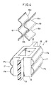
- an integrated circuit package comprises a multilayer ceramic substrate 1 and a plurality of integrated circuit chips 2 mounted on the upper surface of the multilayer substrate 1.
- An array of coaxial pins 3 of identical construction are brazed to connecting pads on the lower surface of the substrate 1.
- Multilayer substrate 1 is fabricated by a known multilayer ceramic technology in which a ceramic slurry of a ceramic powder (mixture of alumina and glass) and polymer binder is first prepared, then cast into thin sheets by passing through sheet forming machines. After drying, the sheets are cut to size, via holes are mechanically punched into the sheet, and custom wiring paths are formed by screening a slurry of tungsten or molybdenum onto the surface of the sheet and the via holes are filled with metal.
- Several of these sheets are precisely aligned and press-laminated together and the entire structure is fired at an elevated temperature to form a monolithic sintered body.
- Multilayer substrate 1 comprises one or more power layers 4 and a ground layer 5. Integrated circuit chips 2 are appropriately connected to power layers 4 and ground layer 5 through terminals 6. Printed circuit patterns 7 are formed between such layers to connect chip terminals 6 to pins 3.
- each of the coaxial pins 3 is constructed of an inner conductor 8 and an outer conductor 9 having either a circular or rectangular cross-section.
- Coaxial pins 3 function as input/output pins or power pins.
- the inner conductor 8 of each input/output pin is connected to an appropriate circuit pattern 7 and the inner conductor 8 of each power pin is connected to one of the power layers 4.
- the outer conductors 9 of both input/output pins and power pins are connected to the gound layer 5. Brazing technique is used to accomplish such electrical connections.
- each input/output pin 3 Since the inner conductor 8 of each input/output pin 3 is electrically shielded by the outer conductor 9 which is grounded, the present invention completely eliminates waveform distortion and crosstalk which would otherwise occur as a result of high speed processing of signals.
- a further advantage of this invention is that since ground connection is integrated with either input/output connection and power connection, the coaxial pins 3 can be arranged in a given area with a higher packing density than that achieved with the prior art pin construction.
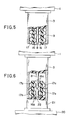
- Figs. 3 to 6 are illustrations of an embodiment which facilitates connection of the coaxial pins 3 to a mother board.
- coaxial pins 3 are arranged in a matrix of rows and columns and each pin is of a rectangular construction and formed with a pair of slits 10 on opposite walls, the slits 10 being aligned with those of adjacent pins 3.
- a pin connector 11 which comprises a series of connector sections 12 which are interconnected by insulative coupling sections or arms 13.
- each connector section 12 is formed of opposed side portions 14 and opposed end portions 15 both of insulative material.
- Inner electrical spring contacts 16 are secured one on each inner wall of side portions 14 and outer electrical spring contacts 17 are secured one on each outer wall of side portions 14.
- Each of the inner contacts 16 has an upper contact portion 16a and a lower contact portion 16b.
- each of the outer contacts 17 has an upper contact portion 17a and a lower contact portion 17b.
- connector sections 12 Prior to connection to a mother board, connector sections 12 are respectively engaged with coaxial pins 3 of each row as shown in Fig. 5, with the coupling sections 13 being slidably fitted into the slits 10 of the corresponding pin 3, and the inner and outer spring contacts 16 and 17 being in pressure contact with the inner and outer conductors 8 and 9 of the corresponding coaxial pin 3, respectively.
- a mother board 20 is provided with an array of coaxial pins 21 identical in construction to the coaxial pins 3 and arranged in positions corresponding to associated coaxial pins 3.
- Each coaxial pin 21 of the mother board has an inner conductor 22 and an outer conductor 23 of the same size as the inner and outer conductors of the corresponding coaxial pin 3.
- the outer conductor 23 of each coaxial pin 21 is formed with slits 24 in positions which aligns with the slits 10 of the corresponding coaxial pin 3.
- the lower contact portions 16b of inner contacts 16 are brought into pressure contact with the inner conductor 22 of coaxial pin 21 with the upper contact portions 16a remaining in pressure contact with the inner conductor 8 of coaxial pin 3, and the lower contact portions 17b of outer contacts 17 are brought into pressure contact with the outer conductor 23 of coaxial pin 21 with the upper contact portions 17a remaining in pressure contact with the outer conductor 9 of coaxial pin 3, whereby electrical connections are established between the inner conductors 8 and 22 and between the outer conductors 9 and 23 of the corresponding pins.
Landscapes
- Production Of Multi-Layered Print Wiring Board (AREA)
- Coupling Device And Connection With Printed Circuit (AREA)
Applications Claiming Priority (2)
| Application Number | Priority Date | Filing Date | Title |
|---|---|---|---|
| JP61200788A JPH0734455B2 (ja) | 1986-08-27 | 1986-08-27 | 多層配線基板 |
| JP200788/86 | 1986-08-27 |
Publications (3)
| Publication Number | Publication Date |
|---|---|
| EP0258056A2 true EP0258056A2 (de) | 1988-03-02 |
| EP0258056A3 EP0258056A3 (en) | 1988-09-07 |
| EP0258056B1 EP0258056B1 (de) | 1991-11-06 |
Family
ID=16430200
Family Applications (1)
| Application Number | Title | Priority Date | Filing Date |
|---|---|---|---|
| EP87307594A Expired EP0258056B1 (de) | 1986-08-27 | 1987-08-27 | Integrierte Schaltungsstruktur mit coaxialen Stiften |
Country Status (6)
| Country | Link |
|---|---|
| US (1) | US4819131A (de) |
| EP (1) | EP0258056B1 (de) |
| JP (1) | JPH0734455B2 (de) |
| AU (1) | AU592518B2 (de) |
| CA (1) | CA1269763A (de) |
| DE (1) | DE3774370D1 (de) |
Cited By (2)
| Publication number | Priority date | Publication date | Assignee | Title |
|---|---|---|---|---|
| GB2225670A (en) * | 1988-11-30 | 1990-06-06 | Hitachi Ltd | Carrier substrate for electrical circuit element |
| AT1695U1 (de) * | 1996-07-29 | 1997-09-25 | Mikroelektronik Ges Mit Beschr | Schaltanordnung |
Families Citing this family (20)
| Publication number | Priority date | Publication date | Assignee | Title |
|---|---|---|---|---|
| JPH0821450B2 (ja) * | 1987-10-05 | 1996-03-04 | 日本電気株式会社 | 高速信号用コネクタ |
| JPH0519995Y2 (de) * | 1988-01-05 | 1993-05-25 | ||
| JPH0677469B2 (ja) * | 1988-12-28 | 1994-09-28 | 日本電気株式会社 | 多接点コネクタの案内構造 |
| US4912772A (en) * | 1989-03-06 | 1990-03-27 | International Business Machines Corporation | Connector and circuit package apparatus for pin array circuit module and circuit board |
| JPH0744240B2 (ja) * | 1990-11-30 | 1995-05-15 | 工業技術院長 | マザーボードとチップキャリアの接続方法 |
| JPH04351710A (ja) * | 1991-05-30 | 1992-12-07 | Sony Corp | 回転ヘッドドラム装置 |
| US5334030A (en) * | 1992-06-01 | 1994-08-02 | National Semiconductor Corporation | PCMCIA bus extender card for PCMCIA system development |
| JPH06314580A (ja) * | 1992-08-05 | 1994-11-08 | Amp Japan Ltd | 二基板接続用同軸コネクタ |
| JPH0828244B2 (ja) * | 1993-04-28 | 1996-03-21 | 日本電気株式会社 | マルチチップパッケージの給電構造 |
| US5791911A (en) * | 1996-10-25 | 1998-08-11 | International Business Machines Corporation | Coaxial interconnect devices and methods of making the same |
| US6137693A (en) * | 1998-07-31 | 2000-10-24 | Agilent Technologies Inc. | High-frequency electronic package with arbitrarily-shaped interconnects and integral shielding |
| US20040043644A1 (en) * | 1999-11-02 | 2004-03-04 | Dibene J. Ted | Coaxial and linear power delivery devices |
| US6803650B2 (en) * | 2001-02-23 | 2004-10-12 | Silicon Bandwidth Inc. | Semiconductor die package having mesh power and ground planes |
| DE10164799B4 (de) * | 2001-03-21 | 2006-03-30 | Audioton Kabelwerk Gmbh | Mobiltelefoneinrichtung mit mehradrigen elektrischen Verbindungseinrichtungen |
| US20040173894A1 (en) * | 2001-09-27 | 2004-09-09 | Amkor Technology, Inc. | Integrated circuit package including interconnection posts for multiple electrical connections |
| US6954984B2 (en) * | 2002-07-25 | 2005-10-18 | International Business Machines Corporation | Land grid array structure |
| JP4771808B2 (ja) * | 2003-09-24 | 2011-09-14 | イビデン株式会社 | 半導体装置 |
| US7544070B2 (en) * | 2004-07-02 | 2009-06-09 | Seagate Technology Llc | Electrical connector defining a power plane |
| US8064224B2 (en) * | 2008-03-31 | 2011-11-22 | Intel Corporation | Microelectronic package containing silicon patches for high density interconnects, and method of manufacturing same |
| US8465297B2 (en) | 2010-09-25 | 2013-06-18 | Intel Corporation | Self referencing pin |
Family Cites Families (7)
| Publication number | Priority date | Publication date | Assignee | Title |
|---|---|---|---|---|
| US3698082A (en) * | 1966-04-25 | 1972-10-17 | Texas Instruments Inc | Complex circuit array method |
| US4231629A (en) * | 1979-01-18 | 1980-11-04 | Telex Computer Products, Inc. | Apparatus for connection of coaxial cables to a printed circuit mother board |
| NL8303268A (nl) * | 1983-09-23 | 1985-04-16 | Philips Nv | Werkwijze ter vervaardiging van een halfgeleiderinrichting en halfgeleiderinrichting vervaardigd door toepassing van een dergelijke werkwijze. |
| US4612601A (en) * | 1983-11-30 | 1986-09-16 | Nec Corporation | Heat dissipative integrated circuit chip package |
| US4692839A (en) * | 1985-06-24 | 1987-09-08 | Digital Equipment Corporation | Multiple chip interconnection system and package |
| SE450065B (sv) * | 1985-10-03 | 1987-06-01 | Ericsson Telefon Ab L M | Koaxialkontakt avsedd att anvendas vid en overgang mellan en koaxialledare och en planledare |
| US4814855A (en) * | 1986-04-29 | 1989-03-21 | International Business Machines Corporation | Balltape structure for tape automated bonding, multilayer packaging, universal chip interconnection and energy beam processes for manufacturing balltape |
-
1986
- 1986-08-27 JP JP61200788A patent/JPH0734455B2/ja not_active Expired - Lifetime
-
1987
- 1987-08-26 US US07/089,530 patent/US4819131A/en not_active Expired - Fee Related
- 1987-08-26 CA CA000545375A patent/CA1269763A/en not_active Expired
- 1987-08-27 DE DE8787307594T patent/DE3774370D1/de not_active Expired - Lifetime
- 1987-08-27 AU AU77632/87A patent/AU592518B2/en not_active Ceased
- 1987-08-27 EP EP87307594A patent/EP0258056B1/de not_active Expired
Cited By (3)
| Publication number | Priority date | Publication date | Assignee | Title |
|---|---|---|---|---|
| GB2225670A (en) * | 1988-11-30 | 1990-06-06 | Hitachi Ltd | Carrier substrate for electrical circuit element |
| GB2225670B (en) * | 1988-11-30 | 1992-08-19 | Hitachi Ltd | Carrier substrate and method for preparing the same |
| AT1695U1 (de) * | 1996-07-29 | 1997-09-25 | Mikroelektronik Ges Mit Beschr | Schaltanordnung |
Also Published As
| Publication number | Publication date |
|---|---|
| JPS6356949A (ja) | 1988-03-11 |
| EP0258056B1 (de) | 1991-11-06 |
| JPH0734455B2 (ja) | 1995-04-12 |
| AU7763287A (en) | 1988-03-03 |
| EP0258056A3 (en) | 1988-09-07 |
| US4819131A (en) | 1989-04-04 |
| CA1269763A (en) | 1990-05-29 |
| AU592518B2 (en) | 1990-01-11 |
| DE3774370D1 (de) | 1991-12-12 |
Similar Documents
| Publication | Publication Date | Title |
|---|---|---|
| US4819131A (en) | Integrated circuit package having coaxial pins | |
| US5007841A (en) | Integrated-circuit chip interconnection system | |
| CA1143862A (en) | High performance semiconductor package assembly | |
| US5593322A (en) | Leadless high density connector | |
| US5701233A (en) | Stackable modules and multimodular assemblies | |
| US4581679A (en) | Multi-element circuit construction | |
| US5006673A (en) | Fabrication of pad array carriers from a universal interconnect structure | |
| US4739125A (en) | Electric component part having lead terminals | |
| JP4567038B2 (ja) | 高速差動信号エッジカードコネクタの回路基板レイアウト | |
| US4574331A (en) | Multi-element circuit construction | |
| EP0309942A2 (de) | Keramische Mehrschichtpackung mit Hochfrequenzverbindungen | |
| US5019945A (en) | Backplane interconnection system | |
| EP0357758B1 (de) | Hermetische packung für integrierte schaltungschips | |
| US4772864A (en) | Multilayer circuit prototyping board | |
| EP0282693B1 (de) | Steckbares Gehäuse integrierter Schaltungen | |
| GB2341980A (en) | Circuit board connection device | |
| US4695810A (en) | Waffleline-configured microwave transmission link | |
| US4874086A (en) | Film carrier and a method for manufacturing a semiconductor device utilizing the same | |
| US5861664A (en) | LSI package and manufacturing method thereof | |
| JP3084209B2 (ja) | 電子コンポーネントおよびその製造方法 | |
| US4583150A (en) | Printed circuit boards | |
| EP0569528A4 (en) | Electrical connectors | |
| EP0444820A2 (de) | MMIC-Gehäuse und Anschluss | |
| US4851793A (en) | Waffleline - configured transmission link | |
| JP2564297B2 (ja) | 回路基板 |
Legal Events
| Date | Code | Title | Description |
|---|---|---|---|
| PUAI | Public reference made under article 153(3) epc to a published international application that has entered the european phase |
Free format text: ORIGINAL CODE: 0009012 |
|
| 17P | Request for examination filed |
Effective date: 19870903 |
|
| AK | Designated contracting states |
Kind code of ref document: A2 Designated state(s): BE DE FR GB IT NL SE |
|
| PUAL | Search report despatched |
Free format text: ORIGINAL CODE: 0009013 |
|
| AK | Designated contracting states |
Kind code of ref document: A3 Designated state(s): BE DE FR GB IT NL SE |
|
| 17Q | First examination report despatched |
Effective date: 19900426 |
|
| GRAA | (expected) grant |
Free format text: ORIGINAL CODE: 0009210 |
|
| AK | Designated contracting states |
Kind code of ref document: B1 Designated state(s): BE DE FR GB IT NL SE |
|
| REF | Corresponds to: |
Ref document number: 3774370 Country of ref document: DE Date of ref document: 19911212 |
|
| ET | Fr: translation filed | ||
| ITF | It: translation for a ep patent filed | ||
| PLBE | No opposition filed within time limit |
Free format text: ORIGINAL CODE: 0009261 |
|
| STAA | Information on the status of an ep patent application or granted ep patent |
Free format text: STATUS: NO OPPOSITION FILED WITHIN TIME LIMIT |
|
| 26N | No opposition filed | ||
| EAL | Se: european patent in force in sweden |
Ref document number: 87307594.9 |
|
| PGFP | Annual fee paid to national office [announced via postgrant information from national office to epo] |
Ref country code: BE Payment date: 19960723 Year of fee payment: 10 |
|
| PGFP | Annual fee paid to national office [announced via postgrant information from national office to epo] |
Ref country code: GB Payment date: 19960806 Year of fee payment: 10 |
|
| PGFP | Annual fee paid to national office [announced via postgrant information from national office to epo] |
Ref country code: FR Payment date: 19960807 Year of fee payment: 10 |
|
| PGFP | Annual fee paid to national office [announced via postgrant information from national office to epo] |
Ref country code: SE Payment date: 19960821 Year of fee payment: 10 |
|
| PGFP | Annual fee paid to national office [announced via postgrant information from national office to epo] |
Ref country code: DE Payment date: 19961022 Year of fee payment: 10 |
|
| PG25 | Lapsed in a contracting state [announced via postgrant information from national office to epo] |
Ref country code: GB Free format text: LAPSE BECAUSE OF NON-PAYMENT OF DUE FEES Effective date: 19970827 |
|
| PG25 | Lapsed in a contracting state [announced via postgrant information from national office to epo] |
Ref country code: SE Free format text: LAPSE BECAUSE OF NON-PAYMENT OF DUE FEES Effective date: 19970828 |
|
| PG25 | Lapsed in a contracting state [announced via postgrant information from national office to epo] |
Ref country code: BE Free format text: LAPSE BECAUSE OF NON-PAYMENT OF DUE FEES Effective date: 19970831 |
|
| PGFP | Annual fee paid to national office [announced via postgrant information from national office to epo] |
Ref country code: NL Payment date: 19971231 Year of fee payment: 11 |
|
| BERE | Be: lapsed |
Owner name: NEC CORP. Effective date: 19970831 |
|
| PG25 | Lapsed in a contracting state [announced via postgrant information from national office to epo] |
Ref country code: NL Free format text: LAPSE BECAUSE OF NON-PAYMENT OF DUE FEES Effective date: 19980301 |
|
| GBPC | Gb: european patent ceased through non-payment of renewal fee |
Effective date: 19970827 |
|
| PG25 | Lapsed in a contracting state [announced via postgrant information from national office to epo] |
Ref country code: FR Free format text: LAPSE BECAUSE OF NON-PAYMENT OF DUE FEES Effective date: 19980430 |
|
| PG25 | Lapsed in a contracting state [announced via postgrant information from national office to epo] |
Ref country code: DE Free format text: LAPSE BECAUSE OF NON-PAYMENT OF DUE FEES Effective date: 19980501 |
|
| EUG | Se: european patent has lapsed |
Ref document number: 87307594.9 |
|
| NLV4 | Nl: lapsed or anulled due to non-payment of the annual fee |
Effective date: 19980301 |
|
| REG | Reference to a national code |
Ref country code: FR Ref legal event code: ST |
|
| PG25 | Lapsed in a contracting state [announced via postgrant information from national office to epo] |
Ref country code: IT Free format text: LAPSE BECAUSE OF NON-PAYMENT OF DUE FEES Effective date: 20050827 |