EP0258148A2 - Modification des propriétés de dopants de type p avec d'autres dopants du type p - Google Patents
Modification des propriétés de dopants de type p avec d'autres dopants du type p Download PDFInfo
- Publication number
- EP0258148A2 EP0258148A2 EP87401927A EP87401927A EP0258148A2 EP 0258148 A2 EP0258148 A2 EP 0258148A2 EP 87401927 A EP87401927 A EP 87401927A EP 87401927 A EP87401927 A EP 87401927A EP 0258148 A2 EP0258148 A2 EP 0258148A2
- Authority
- EP
- European Patent Office
- Prior art keywords
- type
- impurities
- boron
- region
- gallium
- Prior art date
- Legal status (The legal status is an assumption and is not a legal conclusion. Google has not performed a legal analysis and makes no representation as to the accuracy of the status listed.)
- Granted
Links
Images


Classifications
-
- H—ELECTRICITY
- H10—SEMICONDUCTOR DEVICES; ELECTRIC SOLID-STATE DEVICES NOT OTHERWISE PROVIDED FOR
- H10P—GENERIC PROCESSES OR APPARATUS FOR THE MANUFACTURE OR TREATMENT OF DEVICES COVERED BY CLASS H10
- H10P30/00—Ion implantation into wafers, substrates or parts of devices
- H10P30/20—Ion implantation into wafers, substrates or parts of devices into semiconductor materials, e.g. for doping
- H10P30/202—Ion implantation into wafers, substrates or parts of devices into semiconductor materials, e.g. for doping characterised by the semiconductor materials
- H10P30/204—Ion implantation into wafers, substrates or parts of devices into semiconductor materials, e.g. for doping characterised by the semiconductor materials into Group IV semiconductors
-
- H—ELECTRICITY
- H10—SEMICONDUCTOR DEVICES; ELECTRIC SOLID-STATE DEVICES NOT OTHERWISE PROVIDED FOR
- H10P—GENERIC PROCESSES OR APPARATUS FOR THE MANUFACTURE OR TREATMENT OF DEVICES COVERED BY CLASS H10
- H10P30/00—Ion implantation into wafers, substrates or parts of devices
- H10P30/20—Ion implantation into wafers, substrates or parts of devices into semiconductor materials, e.g. for doping
- H10P30/21—Ion implantation into wafers, substrates or parts of devices into semiconductor materials, e.g. for doping of electrically active species
- H10P30/212—Through-implantation
-
- H—ELECTRICITY
- H10—SEMICONDUCTOR DEVICES; ELECTRIC SOLID-STATE DEVICES NOT OTHERWISE PROVIDED FOR
- H10P—GENERIC PROCESSES OR APPARATUS FOR THE MANUFACTURE OR TREATMENT OF DEVICES COVERED BY CLASS H10
- H10P32/00—Diffusion of dopants within, into or out of wafers, substrates or parts of devices
Definitions
- the present invention is directed to monolithic integrated circuits, and in particular to the characteristics of p-type regions in integrated circuit devices.
- a PMOS field-effect transistor comprises an n-type substrate having p-type source and drain regions formed at its surface.
- the n-type activity in the substrate is provided by doping a layer of silicon with a donor (Group V) impurity such as arsenic or phosphorous.
- the source and drain p-type regions are then formed by diffusing an acceptor (Group III) impurity, most notably boron, into two predetermined regions of the substrate.
- p-type impurities have relatively high diffusion coefficients.
- p-type impurity atoms tend to move a relatively great distance in the silicon. Consequently, the transistor must be large enough in size to accommodate the relatively large volumes occupied by the p-type source and drain regions and yet provide the desired electrical activity.
- p-type dopants it is desirable to provide a technique for limiting the diffusion depth of p-type dopants to thereby enable smaller integrated circuit devices to be fabricated.
- One possible way to achieve this objective is to reduce the concentration of impurity atoms that are employed in the p-type region. Such an approach would enable shallower source and drain regions to be formed, for example. However, this approach is not without attendant limitations. In particular, these shallower regions of lower concentration exhibit increased electrical resistance, which compromises the electrical performance characteristics of the transistor. For example, the transistor might operate slower than a similar transistor with deeper and more highly concentrated p-type regions.
- one p-type dopant to modify the diffusion characteristics of another p-type dopant.
- a limited amount of gallium can be implanted into a p-type region to a limited depth along with a greater amount of boron to confine the diffusion of the boron, and thereby produce smaller devices.
- the resulting region exhibits electrical activity that is greater than the simple additive behavior of boron and gallium acting alone.
- the control over the diffusion of the boron comes about from an attraction between the boron and the gallium during diffusion.
- the gallium by implanting the gallium with a relatively low amount of energy so that the depth of the implant is shallow, i.e., near the surface of a silicon substrate, the boron's attraction to the gallium will cause it to also remain near the surface during annealing.
- the gallium is deeply implanted at a high energy level, its effect will be to "pull" the boron atoms to greater depths than would normally occur during annealing, thus provided an enhanced diffusion pattern when desired.
- p-type dopants include aluminum-boron, gallium-aluminum, and indium-boron.
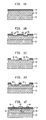
- an n-type channel layer 10 is grown or otherwise suitably formed on a p-type substrate 12.
- An oxide layer 14 is then formed over the channel layer.
- two windows 16 are formed in the oxide layer in the areas where the source and drain regions of the transistor are to be located.
- Gallium ions are implanted through the windows 16 into areas 18 along the surface of the channel layer 10. If desired, a thin layer of oxide can be left in each window in order to provide better control over the depth of the implant.
- the windows 16 are enlarged as shown in Figure 1C. Boron ions are then implanted into areas 20 through these enlarged windows.
- the energy levels that are employed during each of the ion implants are preferably chosen relative to one another so that the depth of the peak concentration is approximately the same for both impurities if it is desired to constrain the diffusion of boron.
- the entire structure is heated for a suitable period of time to cause the gallium and boron ions to simultaneously diffuse into the channel layer 10 and thereby form the source and drain regions 22, as shown in Figure 1D.
- the remainder of the oxide layer 14 is removed and a new oxide layer 24 is formed over the entire structure.
- the height of a portion of the layer 24 overlying the channel region 26 between the source and drain regions is reduced, for example by etching, and a gate electrode 28 is deposited in this area.
- holes are opened over the source and drain regions and contacts 30 are provided for electrical connection of the transistor in a well-known manner.
- CMOS circuits it becomes feasible to first do all n-channel processing and then follow with p-channel processing using lower temperatures or shorter annealing times, since the n-type dopants are not likely to diffuse any further in such a situation.
- Boron ions were implanted into silicon through a layer of thermally grown oxide having a thickness of 250 angstroms.
- the dosage was 3 x 10¹⁴ ions/cm2 and the power level for the implant was 20 KeV.
- the material was then annealed at 900°C for 30 minutes in nitrogen.
- the resulting concentration of p-type carriers had a distribution as shown by curve A in Figure 2A.
- the concentration of boron (atoms/cc) had a distribution as shown by the dashed line curve labelled "B" in Figure 2B.
- Gallium ions were implanted into silicon through a layer of thermally grown oxide having a thickness of 250 angstroms.
- the dosage was 1 x 10¹⁴ ions/cm2 and the power level for the implant was 110 KeV.
- the material was then annealed at 900°C for 30 minutes in nitrogen.
- the resulting concentration of p-type carriers had a distribution as shown by curve B in Figure 2A, and the gallium atoms were distributed as shown by the dashed line labelled "Ga" in Figure 2B.
- Example 2 The same area of silicon substrate was implanted with boron ions as described in Example 1 and gallium ions were implanted as described in Example 2. The combined implants were then annealed at 900°C for 30 minutes in nitrogen.
- the resulting concentration of p-type carriers had a distribution as shown by curve C in Figure 2A.
- the boron and gallium atoms had a distribution as represented by the two respective solid line curves in Figure 2B. From these curves it can be seen that the two p-type dopants attract one another when they are paired and anneal together. This relative attraction results in the peak concentration of carriers being significantly closer to the surface of the substrate than with either impurity used alone. Accordingly, shallower p-type regions can be formed without increasing inherent resistance.
- the power levels of the implants are such that the projected range, R p , of penetration of the ions are approximately the same for both boron and gallium. This is done to constrain the depth of boron during annealing.
- the mutual attraction of the two dopants can be used to impart other characteristics to the device, as shown in the following examples.
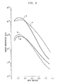
- Boron ions were implanted into a silicon substrate at a dosage of 3 x 10¹⁴ ions/cm2 and a power level of 40 KeV. After annealing at 900°C for 30 minutes, the boron atoms had a distribution as shown by the dashed line curve "B" of Figure 3.
- Gallium ions were implanted into a silicon substrate at a dosage of 1 x 10¹⁴ ion/cm2 and a power level of 60 KeV. After annealing, the distribution of gallium ions is shown by the dashed line curve "Ga" of Figure 3.
- the projected range of the boron implant is much greater than that of the gallium implant (e.g., about 640 ⁇ deeper).
- the boron ions tend to "pull" the gallium ions deeper into the substrate during annealing. Such an ability to influence the diffusion of the gallium may be desirable in certain situations.
- boron and gallium Although described with particular reference to the combination of boron and gallium, the concepts underlying the invention are not limited to these specific p-type dopants. For example, a combination of aluminum or indium with either boron or gallium also results in interactions which provide the same advantageous characteristics.
- Figure 4 illustrates the particular results that are achieved when aluminum and boron are paired to form the p-type impurity.
- Curve A in Figure 4 depicts the carrier concentration when boron alone is implanted with a dose of 6 x 10¹⁵ at 50 KeV and annealed at 950°C under neutral ambient conditions for 60 minutes.
- Curve B shows the carrier concentration when aluminum alone is implanted with a dose of 4 x 10¹⁵ at 100 KeV and annealed at 950°C under neutral ambient conditions for 60 minutes.
- Curve C shows the carrier concentration profile that is substantially closer to the surface of the silicon than boron alone.
Landscapes
- Metal-Oxide And Bipolar Metal-Oxide Semiconductor Integrated Circuits (AREA)
- Insulated Gate Type Field-Effect Transistor (AREA)
- Crystals, And After-Treatments Of Crystals (AREA)
- Led Devices (AREA)
- Materials For Photolithography (AREA)
Applications Claiming Priority (2)
| Application Number | Priority Date | Filing Date | Title |
|---|---|---|---|
| US06/901,502 US4746964A (en) | 1986-08-28 | 1986-08-28 | Modification of properties of p-type dopants with other p-type dopants |
| US901502 | 1997-07-28 |
Publications (3)
| Publication Number | Publication Date |
|---|---|
| EP0258148A2 true EP0258148A2 (fr) | 1988-03-02 |
| EP0258148A3 EP0258148A3 (en) | 1988-06-01 |
| EP0258148B1 EP0258148B1 (fr) | 1992-06-03 |
Family
ID=25414313
Family Applications (1)
| Application Number | Title | Priority Date | Filing Date |
|---|---|---|---|
| EP87401927A Expired - Lifetime EP0258148B1 (fr) | 1986-08-28 | 1987-08-25 | Modification des propriétés de dopants de type p avec d'autres dopants du type p |
Country Status (5)
| Country | Link |
|---|---|
| US (1) | US4746964A (fr) |
| EP (1) | EP0258148B1 (fr) |
| JP (1) | JPS6362227A (fr) |
| KR (1) | KR880003404A (fr) |
| DE (1) | DE3779523T2 (fr) |
Cited By (4)
| Publication number | Priority date | Publication date | Assignee | Title |
|---|---|---|---|---|
| EP0359852A1 (fr) * | 1988-09-21 | 1990-03-28 | Siemens Aktiengesellschaft | Procédé de fabrication de régions dopées peu profondes ayant une faible résistance de couche dans un substrat en silicium |
| EP0397014A3 (fr) * | 1989-05-10 | 1991-02-06 | National Semiconductor Corporation | Caisson P dopé à l'aluminium et au bore |
| EP0707345A1 (fr) * | 1994-10-11 | 1996-04-17 | Advanced Micro Devices, Inc. | Procédé de fabrication d'un circuit intégré |
| WO1999050900A1 (fr) * | 1998-03-30 | 1999-10-07 | Advanced Micro Devices, Inc. | Transistor a drain faiblement dope a longueur de canal reduite utilisant un implant subamorphe a grand angle d'inclinaison aux fins d'une meilleure diffusion laterale |
Families Citing this family (14)
| Publication number | Priority date | Publication date | Assignee | Title |
|---|---|---|---|---|
| TW399774U (en) * | 1989-07-03 | 2000-07-21 | Gen Electric | FET, IGBT and MCT structures to enhance operating characteristics |
| JPH0797590B2 (ja) * | 1989-11-21 | 1995-10-18 | 株式会社東芝 | バイポーラトランジスタの製造方法 |
| US5137838A (en) * | 1991-06-05 | 1992-08-11 | National Semiconductor Corporation | Method of fabricating P-buried layers for PNP devices |
| US5192712A (en) * | 1992-04-15 | 1993-03-09 | National Semiconductor Corporation | Control and moderation of aluminum in silicon using germanium and germanium with boron |
| US5825052A (en) * | 1994-08-26 | 1998-10-20 | Rohm Co., Ltd. | Semiconductor light emmitting device |
| JP2002076332A (ja) * | 2000-08-24 | 2002-03-15 | Hitachi Ltd | 絶縁ゲート型電界効果トランジスタ及びその製造方法 |
| US6660608B1 (en) * | 2002-02-25 | 2003-12-09 | Advanced Micro Devices, Inc. | Method for manufacturing CMOS device having low gate resistivity using aluminum implant |
| US6599831B1 (en) * | 2002-04-30 | 2003-07-29 | Advanced Micro Devices, Inc. | Metal gate electrode using silicidation and method of formation thereof |
| US20040121524A1 (en) * | 2002-12-20 | 2004-06-24 | Micron Technology, Inc. | Apparatus and method for controlling diffusion |
| US7297617B2 (en) * | 2003-04-22 | 2007-11-20 | Micron Technology, Inc. | Method for controlling diffusion in semiconductor regions |
| US8110469B2 (en) | 2005-08-30 | 2012-02-07 | Micron Technology, Inc. | Graded dielectric layers |
| JP2008085355A (ja) * | 2007-10-22 | 2008-04-10 | Toshiba Corp | イオン注入方法 |
| US11362221B2 (en) * | 2017-02-06 | 2022-06-14 | Alliance For Sustainable Energy, Llc | Doped passivated contacts |
| CN113178385B (zh) * | 2021-03-31 | 2022-12-23 | 青岛惠科微电子有限公司 | 一种芯片的制造方法、制造设备和芯片 |
Family Cites Families (8)
| Publication number | Priority date | Publication date | Assignee | Title |
|---|---|---|---|---|
| US3798079A (en) * | 1972-06-05 | 1974-03-19 | Westinghouse Electric Corp | Triple diffused high voltage transistor |
| JPS5457861A (en) * | 1977-10-17 | 1979-05-10 | Hitachi Ltd | Manufacture of semiconductor device |
| JPS5492183A (en) * | 1977-12-29 | 1979-07-21 | Fujitsu Ltd | Manufacture of mis type semiconductor device |
| JPS55151349A (en) * | 1979-05-15 | 1980-11-25 | Matsushita Electronics Corp | Forming method of insulation isolating region |
| JPS5673470A (en) * | 1979-11-21 | 1981-06-18 | Chiyou Lsi Gijutsu Kenkyu Kumiai | Manufacture of semiconductor device |
| JPS58106823A (ja) * | 1981-12-18 | 1983-06-25 | Toshiba Corp | イオン注入方法 |
| JPS58111324A (ja) * | 1981-12-25 | 1983-07-02 | Hitachi Ltd | 半導体装置の製造方法 |
| US4512816A (en) * | 1982-02-26 | 1985-04-23 | National Semiconductor Corporation | High-density IC isolation technique capacitors |
-
1986
- 1986-08-28 US US06/901,502 patent/US4746964A/en not_active Expired - Lifetime
-
1987
- 1987-08-21 KR KR870009163A patent/KR880003404A/ko not_active Ceased
- 1987-08-25 EP EP87401927A patent/EP0258148B1/fr not_active Expired - Lifetime
- 1987-08-25 DE DE8787401927T patent/DE3779523T2/de not_active Expired - Fee Related
- 1987-08-28 JP JP62213171A patent/JPS6362227A/ja active Pending
Cited By (7)
| Publication number | Priority date | Publication date | Assignee | Title |
|---|---|---|---|---|
| EP0359852A1 (fr) * | 1988-09-21 | 1990-03-28 | Siemens Aktiengesellschaft | Procédé de fabrication de régions dopées peu profondes ayant une faible résistance de couche dans un substrat en silicium |
| EP0397014A3 (fr) * | 1989-05-10 | 1991-02-06 | National Semiconductor Corporation | Caisson P dopé à l'aluminium et au bore |
| EP0707345A1 (fr) * | 1994-10-11 | 1996-04-17 | Advanced Micro Devices, Inc. | Procédé de fabrication d'un circuit intégré |
| US6331458B1 (en) | 1994-10-11 | 2001-12-18 | Advanced Micro Devices, Inc. | Active region implant methodology using indium to enhance short channel performance of a surface channel PMOS device |
| WO1999050900A1 (fr) * | 1998-03-30 | 1999-10-07 | Advanced Micro Devices, Inc. | Transistor a drain faiblement dope a longueur de canal reduite utilisant un implant subamorphe a grand angle d'inclinaison aux fins d'une meilleure diffusion laterale |
| US5970353A (en) * | 1998-03-30 | 1999-10-19 | Advanced Micro Devices, Inc. | Reduced channel length lightly doped drain transistor using a sub-amorphous large tilt angle implant to provide enhanced lateral diffusion |
| US6593623B1 (en) | 1998-03-30 | 2003-07-15 | Advanced Micro Devices, Inc. | Reduced channel length lightly doped drain transistor using a sub-amorphous large tilt angle implant to provide enhanced lateral diffusion |
Also Published As
| Publication number | Publication date |
|---|---|
| DE3779523T2 (de) | 1993-01-21 |
| DE3779523D1 (de) | 1992-07-09 |
| JPS6362227A (ja) | 1988-03-18 |
| US4746964A (en) | 1988-05-24 |
| KR880003404A (ko) | 1988-05-17 |
| EP0258148B1 (fr) | 1992-06-03 |
| EP0258148A3 (en) | 1988-06-01 |
Similar Documents
| Publication | Publication Date | Title |
|---|---|---|
| US4746964A (en) | Modification of properties of p-type dopants with other p-type dopants | |
| US6221724B1 (en) | Method of fabricating an integrated circuit having punch-through suppression | |
| EP0056856B1 (fr) | Procédé de fabrication de jonctions PN, particulièrement dans les transistors à effet de champ à grille isolée, avec des caractéristiques de tension de drain améliorées | |
| US5783469A (en) | Method for making nitrogenated gate structure for improved transistor performance | |
| US6180476B1 (en) | Dual amorphization implant process for ultra-shallow drain and source extensions | |
| US5268317A (en) | Method of forming shallow junctions in field effect transistors | |
| US5821147A (en) | Integrated circuit fabrication | |
| KR100260044B1 (ko) | 고속/고성능 모스 트랜지스터 및 그 제조방법 | |
| KR20030003690A (ko) | 반도체 장치 및 그 제조 방법 | |
| US6297098B1 (en) | Tilt-angle ion implant to improve junction breakdown in flash memory application | |
| GB2185350A (en) | A method for MOS transistor manufacture | |
| US4502205A (en) | Method of manufacturing an MIS type semiconductor device | |
| JPH06310719A (ja) | Ge−SiのSOI型MOSトランジスタ及びその製造方法 | |
| US6399452B1 (en) | Method of fabricating transistors with low thermal budget | |
| US4839301A (en) | Blanket CMOS channel stop implant employing a combination of n-channel and p-channel punch-through implants | |
| US5677213A (en) | Method for forming a semiconductor device having a shallow junction and a low sheet resistance | |
| US4851360A (en) | NMOS source/drain doping with both P and As | |
| US20040041170A1 (en) | Low dose super deep source/drain implant | |
| EP1011129A2 (fr) | Méthode de fabrication d'un dispositif semiconducteur | |
| JPH0642465B2 (ja) | 浅い接合の形成方法 | |
| US5073509A (en) | Blanket CMOS channel-stop implant | |
| EP1291905A2 (fr) | Procédé pour la fabrication d'un dispositif sémiconducteur | |
| US6410393B1 (en) | Semiconductor device with asymmetric channel dopant profile | |
| US6180470B1 (en) | FETs having lightly doped drain regions that are shaped with counter and noncounter dorant elements | |
| US7157357B2 (en) | Methods of forming halo regions in NMOS transistors |
Legal Events
| Date | Code | Title | Description |
|---|---|---|---|
| PUAI | Public reference made under article 153(3) epc to a published international application that has entered the european phase |
Free format text: ORIGINAL CODE: 0009012 |
|
| AK | Designated contracting states |
Kind code of ref document: A2 Designated state(s): DE FR GB IT NL |
|
| PUAL | Search report despatched |
Free format text: ORIGINAL CODE: 0009013 |
|
| AK | Designated contracting states |
Kind code of ref document: A3 Designated state(s): DE FR GB IT NL |
|
| 17P | Request for examination filed |
Effective date: 19881126 |
|
| 17Q | First examination report despatched |
Effective date: 19901106 |
|
| GRAA | (expected) grant |
Free format text: ORIGINAL CODE: 0009210 |
|
| AK | Designated contracting states |
Kind code of ref document: B1 Designated state(s): DE FR GB IT NL |
|
| REF | Corresponds to: |
Ref document number: 3779523 Country of ref document: DE Date of ref document: 19920709 |
|
| ITF | It: translation for a ep patent filed | ||
| ET | Fr: translation filed | ||
| PLBE | No opposition filed within time limit |
Free format text: ORIGINAL CODE: 0009261 |
|
| STAA | Information on the status of an ep patent application or granted ep patent |
Free format text: STATUS: NO OPPOSITION FILED WITHIN TIME LIMIT |
|
| 26N | No opposition filed | ||
| PGFP | Annual fee paid to national office [announced via postgrant information from national office to epo] |
Ref country code: FR Payment date: 19940812 Year of fee payment: 8 |
|
| PGFP | Annual fee paid to national office [announced via postgrant information from national office to epo] |
Ref country code: NL Payment date: 19940831 Year of fee payment: 8 |
|
| PG25 | Lapsed in a contracting state [announced via postgrant information from national office to epo] |
Ref country code: NL Effective date: 19960301 |
|
| PG25 | Lapsed in a contracting state [announced via postgrant information from national office to epo] |
Ref country code: FR Effective date: 19960430 |
|
| NLV4 | Nl: lapsed or anulled due to non-payment of the annual fee |
Effective date: 19960301 |
|
| REG | Reference to a national code |
Ref country code: FR Ref legal event code: ST |
|
| REG | Reference to a national code |
Ref country code: GB Ref legal event code: IF02 |
|
| PGFP | Annual fee paid to national office [announced via postgrant information from national office to epo] |
Ref country code: GB Payment date: 20040818 Year of fee payment: 18 |
|
| PG25 | Lapsed in a contracting state [announced via postgrant information from national office to epo] |
Ref country code: IT Free format text: LAPSE BECAUSE OF NON-PAYMENT OF DUE FEES;WARNING: LAPSES OF ITALIAN PATENTS WITH EFFECTIVE DATE BEFORE 2007 MAY HAVE OCCURRED AT ANY TIME BEFORE 2007. THE CORRECT EFFECTIVE DATE MAY BE DIFFERENT FROM THE ONE RECORDED. Effective date: 20050825 Ref country code: GB Free format text: LAPSE BECAUSE OF NON-PAYMENT OF DUE FEES Effective date: 20050825 |
|
| PGFP | Annual fee paid to national office [announced via postgrant information from national office to epo] |
Ref country code: DE Payment date: 20050930 Year of fee payment: 19 |
|
| GBPC | Gb: european patent ceased through non-payment of renewal fee |
Effective date: 20050825 |
|
| PG25 | Lapsed in a contracting state [announced via postgrant information from national office to epo] |
Ref country code: DE Free format text: LAPSE BECAUSE OF NON-PAYMENT OF DUE FEES Effective date: 20070301 |